
Templated Synthesis of Diamond Nanopillar Arrays Using Porous Anodic Aluminium Oxide (AAO) Membranes


Abstract
1. Introduction
2. Materials and Methods
2.1. Materials
2.2. Diamond Nanopillar Growth
2.3. Structure and Morphology Characterization
2.4. Stress Modeling
3. Results and Discussion
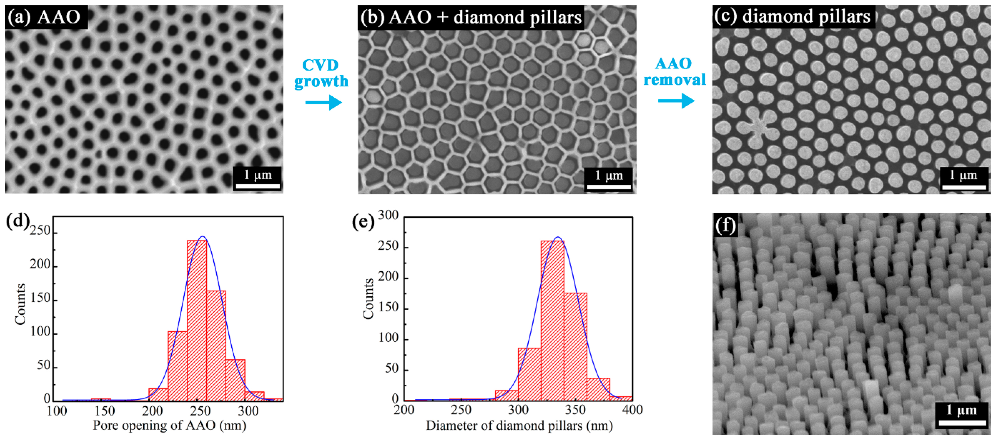
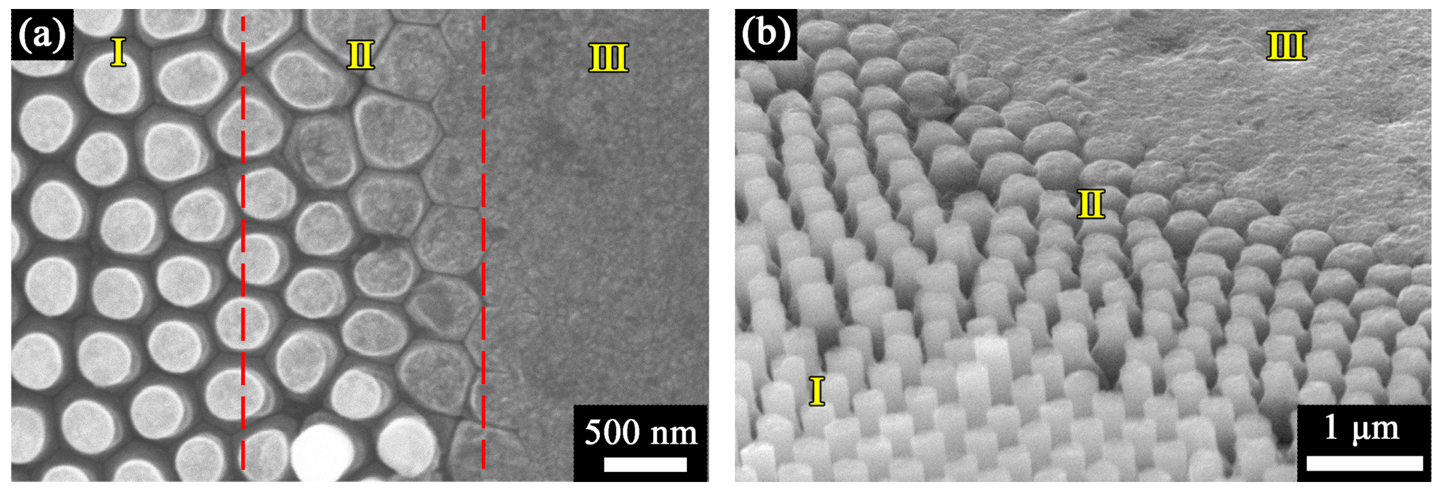
3.1. Growth of Diamond Pillars with ~300 nm Diameter
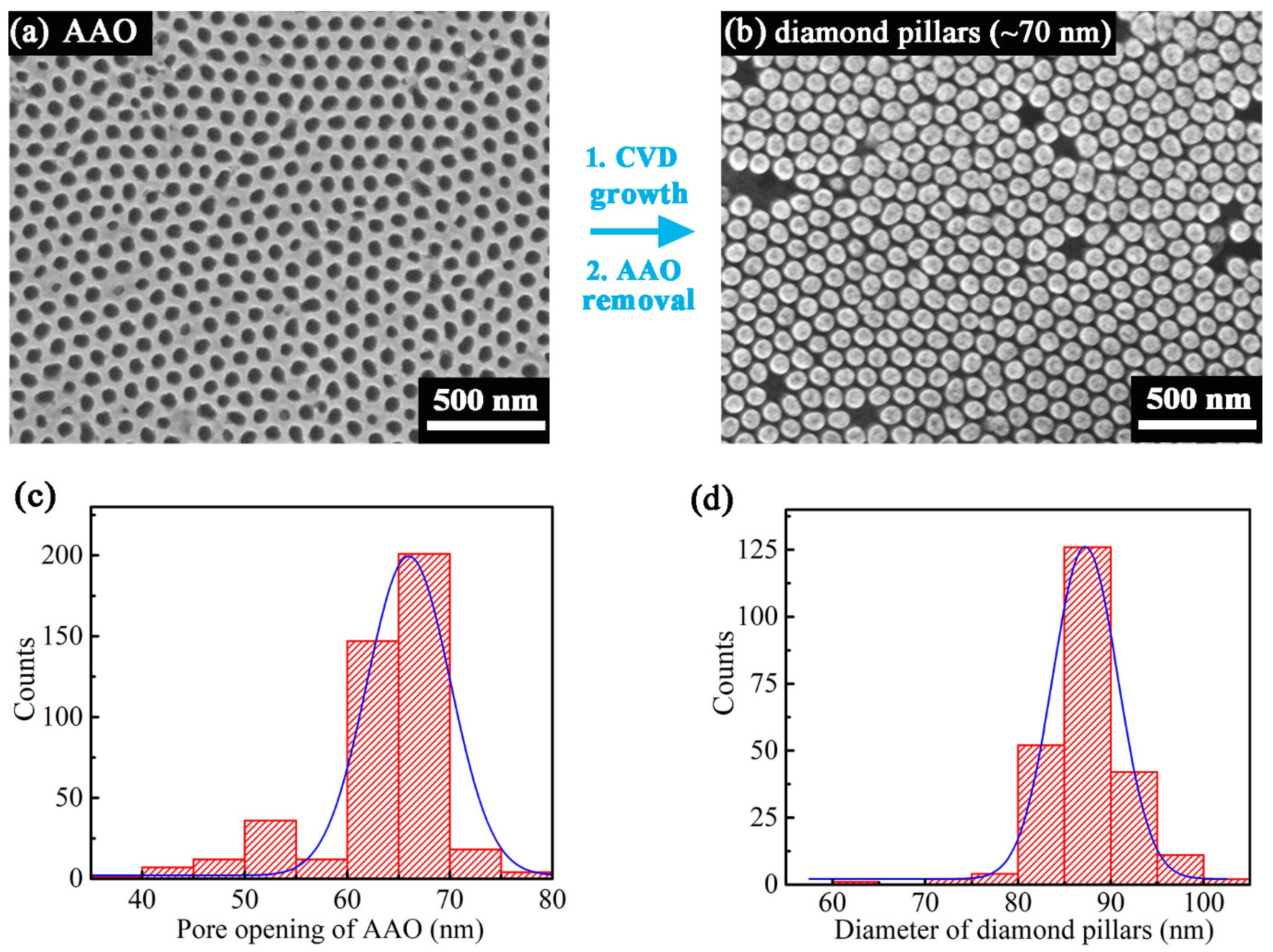
3.2. Growth of Diamond Nanopillars with ~70 nm Diameter
3.3. Raman Spectra and Residual Stress
4. Conclusions
Supplementary Materials
Author Contributions
Funding
Data Availability Statement
Acknowledgments
Conflicts of Interest
References
- Nistor, P.A.; May, P.W. Diamond thin films: Giving biomedical applications a new shine. J. R. Soc. Interface 2017, 14, 20170382. [Google Scholar] [CrossRef] [PubMed]
- Kumar, S.; Huck, A.; Andersen, U.L. Efficient coupling of a single diamond color center to propagating plasmonic gap modes. Nano Lett. 2013, 13, 1221–1225. [Google Scholar] [CrossRef] [PubMed]
- Oliveira, R.C.P.; Buijnsters, J.G.; Mateus, M.M.; Bordado, J.C.M.; Santos, D.M.F. On the electrooxidation of kraft black liquor on boron-doped diamond. J. Electroanal. Chem. 2022, 909, 116151. [Google Scholar] [CrossRef]
- Guo, Z.; Deng, F.; Zhang, L.; Hao, C.; Zhao, X.; Xiang, D. Fabrication and tribological properties of textured diamond coatings on WC-Co cemented carbide surfaces. Ceram. Int. 2021, 47, 5423–5431. [Google Scholar] [CrossRef]
- Chernykh, M.Y.; Andreev, A.A.; Ezubchenko, I.S.; Chernykh, I.A.; Mayboroda, I.O.; Kolobkova, E.M.; Khrapovitskaya, Y.V.; Grishchenko, J.V.; Perminov, P.A.; Sedov, V.S.; et al. GaN-based heterostructures with CVD diamond heat sinks: A new fabrication approach towards efficient electronic devices. Appl. Mater. Today 2022, 26, 101338. [Google Scholar] [CrossRef]
- Ashcheulov, P.; Šebera, J.; Kovalenko, A.; Petrák, V.; Fendrych, F.; Nesládek, M.; Taylor, A.; Živcová, Z.V.; Frank, O.; Kavan, L.; et al. Conductivity of boron-doped polycrystalline diamond films: Influence of specific boron defects. Eur. Phys. J. B 2013, 86, 443. [Google Scholar] [CrossRef]
- Bajaj, P.; Akin, D.; Gupta, A.; Sherman, D.; Shi, B.; Auciello, O.; Bashir, R. Ultrananocrystalline diamond film as an optimal cell interface for biomedical applications. Biomed. Microdevices 2007, 9, 787–794. [Google Scholar] [CrossRef] [PubMed]
- Tao, Y.; Degen, C.L. Single-crystal diamond nanowire tips for ultrasensitive force microscopy. Nano Lett. 2015, 15, 7893–7897. [Google Scholar] [CrossRef]
- Zou, Y.S.; Yang, Y.; Zhang, W.J.; Chong, Y.M.; He, B.; Bello, I.; Lee, S.T. Fabrication of diamond nanopillars and their arrays. Appl. Phys. Lett. 2008, 92, 053105. [Google Scholar] [CrossRef]
- Chen, M.; Best, J.P.; Shorubalko, I.; Michler, J.; Spolenak, R.; Wheeler, J.M. Influence of helium ion irradiation on the structure and strength of diamond. Carbon 2020, 158, 337–345. [Google Scholar] [CrossRef]
- Batzer, M.; Shields, B.; Neu, E.; Widmann, C.; Giese, C.; Nebel, C.; Maletinsky, P. Single crystal diamond pyramids for applications in nanoscale quantum sensing. Opt. Mater. Express 2020, 10, 492–500. [Google Scholar] [CrossRef]
- Yu, Y.; Wu, L.; Zhi, J. Diamond nanowires: Fabrication, structure, properties, and applications. Angew. Chem. Int. Ed. 2014, 53, 14326–14351. [Google Scholar] [CrossRef]
- Castelletto, S.; Rosa, L.; Blackledge, J.; Abri, M.Z.A.; Boretti, A. Advances in diamond nanofabrication for ultrasensitive devices. Microsyst. Nanoeng. 2017, 3, 17061. [Google Scholar] [CrossRef] [PubMed]
- Hsu, C.H.; Cloutier, S.G.; Palefsky, S.; Xu, J. Synthesis of diamond nanowires using atmospheric-pressure chemical vapor deposition. Nano Lett. 2010, 10, 3272–3276. [Google Scholar] [CrossRef]
- Volkova, K.; Heupel, J.; Trofimov, S.; Betz, F.; Colom, R.; MacQueen, R.W.; Akhundzada, S.; Reginka, M.; Ehresmann, A.; Reithmaier, J.P.; et al. Optical and Spin Properties of NV Center Ensembles in Diamond Nano-Pillars. Nanomaterials 2022, 12, 1516. [Google Scholar] [CrossRef] [PubMed]
- Yang, N.; Uetsuka, H.; Nebel, C.E. Biofunctionalization of vertically aligned diamond nanowires. Adv. Funct. Mater. 2009, 19, 887–893. [Google Scholar] [CrossRef]
- Golovanov, A.V.; Luparev, N.V.; Troschiev, S.Y.; Tarelkin, S.A.; Shcherbakova, V.S.; Bormashov, V.S. Two-step reactive ion etching process for diamond-based nanophotonics structure formation. Phys. Status Solidi (a) 2021, 218, 2000206. [Google Scholar] [CrossRef]
- Tan, X.; He, Z.; Yang, Q.; Sun, S.; Jia, H.; Ren, Y. Controllable preparation of single-crystal diamond nanopillar clusters by metal cyclic dewetting process. Appl. Surf. Sci. 2023, 609, 155246. [Google Scholar] [CrossRef]
- Janssen, W.; Faby, S.; Gheeraert, E. Bottom–up fabrication of diamond nanowire arrays. Diam. Relat. Mater. 2011, 20, 779–781. [Google Scholar] [CrossRef]
- Okuyama, S.; Matsushita, S.I.; Fujishima, A. Periodic submicrocylinder diamond surfaces using two-dimensional fine particle arrays. Langmuir 2002, 18, 8282–8287. [Google Scholar] [CrossRef]
- Yang, N.; Uetsuka, H.; Osawa, E.; Nebel, C.E. Vertically aligned nanowires from boron-doped diamond. Nano Lett. 2008, 8, 3572–3576. [Google Scholar] [CrossRef]
- Sun, P.; Tang, C.; Xia, X.; Yao, Z.; Quan, B.; Yuan, G.; Gu, C.; Li, J. Controlled fabrication of periodically high-aspect ratio CVD-diamond nanopillar arrays by pure oxygen etching process. Microelectron. Eng. 2016, 155, 61–66. [Google Scholar] [CrossRef]
- Evtimova, J.; Kulisch, W.; Petkov, C.; Petkov, E.; Schnabel, F.; Reithmaier, J.P.; Popov, C. Reactive ion etching of nanocrystalline diamond for the fabrication of one-dimensional nanopillars. Diam. Relat. Mater. 2013, 36, 58–63. [Google Scholar] [CrossRef]
- Fisher, L.E.; Yang, Y.; Yuen, M.F.; Zhang, W.; Nobbs, A.H.; Su, B. Bactericidal activity of biomimetic diamond nanocone surfaces. Biointerphases 2016, 11, 011014. [Google Scholar] [CrossRef]
- Wei, M.; Terashima, C.; Lv, M.; Fujishima, A.; Gu, Z.Z. Boron-doped diamond nanograss array for electrochemical sensors. Chem. Commun. 2009, 24, 3624–3626. [Google Scholar] [CrossRef]
- Sartori, A.F.; Orlando, S.; Bellucci, A.; Trucchi, D.M.; Abrahami, S.; Boehme, T.; Hantschel, T.; Vandervorst, W.; Buijnsters, J.G. Laser-induced periodic surface structures (LIPSS) on heavily boron-doped diamond for electrode applications. ACS Appl. Mater. Interfaces 2018, 10, 43236–43251. [Google Scholar] [CrossRef] [PubMed]
- Xia, Y.; Yang, P.; Sun, Y.; Wu, Y.; Mayers, B.; Gates, B.; Yin, Y.; Kim, F.; Yan, H. One-dimensional nanostructures: Synthesis, characterization, and applications. Adv. Mater. 2003, 15, 353–389. [Google Scholar] [CrossRef]
- Sun, L.; Gong, J.; Zhu, D.; Zhu, Z.; He, S. Diamond nanorods from carbon nanotubes. Adv. Mater. 2004, 16, 1849–1853. [Google Scholar] [CrossRef]
- Hsu, C.H.; Xu, J. Diamond nanowire—A challenge from extremes. Nanoscale 2012, 4, 5293–5299. [Google Scholar] [CrossRef]
- Luo, D.; Wu, L.; Zhi, J. Fabrication of boron-doped diamond nanorod forest electrodes and their application in nonenzymatic amperometric glucose biosensing. ACS Nano 2009, 3, 2121–2128. [Google Scholar] [CrossRef]
- Sulka, G.D.; Brzózka, A.; Zaraska, L.; Wierzbicka, E.; Brudzisz, A. AAO templates with different patterns and channel shapes. In Submicron Porous Materials; Bettotti, P., Ed.; Springer: Cham, Switzerland, 2017; pp. 107–156. [Google Scholar] [CrossRef]
- Hnida, K.; Mech, J.; Sulka, G.D. Template-assisted electrodeposition of indium–antimony nanowires–Comparison of electrochemical methods. Appl. Surf. Sci. 2013, 287, 252–256. [Google Scholar] [CrossRef]
- Buijnsters, J.G.; Zhong, R.; Tsyntsaru, N.; Celis, J.P. Surface Wettability of Macroporous Anodized Aluminum Oxide. ACS Appl. Mater. Interfaces 2013, 5, 3224–3233. [Google Scholar] [CrossRef] [PubMed]
- Masuda, H.; Watanabe, M.; Yasui, K.; Tryk, D.; Rao, T.; Fujishima, A. Fabrication of a nanostructured diamond honeycomb film. Adv. Mater. 2000, 12, 444–447. [Google Scholar] [CrossRef]
- Hao, Q.; Huang, H.; Fan, X.; Yin, Y.; Wang, J.; Li, W.; Qiu, T.; Ma, L.; Chu, P.K.; Schmidt, O.G. Controlled patterning of plasmonic dimers by using an ultrathin nanoporous alumina membrane as a shadow mask. ACS Appl. Mater. Interfaces 2017, 9, 36199–36205. [Google Scholar] [CrossRef]
- Lee, W.; Park, S.J. Porous anodic aluminum oxide: Anodization and templated synthesis of functional nanostructures. Chem. Rev. 2014, 114, 7487–7556. [Google Scholar] [CrossRef] [PubMed]
- Wang, Y.; Shen, Y.; Xu, W.; Xu, S.; Li, H. A unique patterned diamond stamp for a periodically hierarchical nanoarray structure. Nanotechnology 2016, 27, 434001. [Google Scholar] [CrossRef] [PubMed]
- Masuda, H.; Yanagishita, T.; Yasui, K.; Nishio, K.; Yagi, I.; Rao, T.N.; Fujishima, A. Synthesis of Well-Aligned Diamond Nanocylinders. Adv. Mater. 2001, 13, 247–249. [Google Scholar] [CrossRef]
- Yanagishita, T.; Nishio, K.; Nakao, M.; Fujishima, A.; Masuda, H. Synthesis of diamond cylinders with triangular and square cross sections using anodic porous alumina templates. Chem. Lett. 2002, 31, 976–977. [Google Scholar] [CrossRef]
- Sartori, A.F.; Overes, B.H.; Fanzio, P.; Tsigkourakos, M.; Sasso, L.; Buijnsters, J.G. Template-assisted bottom-up growth of nanocrystalline diamond micropillar arrays. Diam. Relat. Mater. 2019, 95, 20–27. [Google Scholar] [CrossRef]
- Buijnsters, J.G.; Tsigkourakos, M.; Hantschel, T.; Gomes, F.O.V.; Nuytten, T.; Favia, P.; Bender, H.; Arstila, K.; Celis, J.P.; Vandervorst, W. Effect of Boron Doping on the Wear Behavior of the Growth and Nucleation Surfaces of Micro- and Nanocrystalline Diamond Films. ACS Appl. Mater. Interfaces 2016, 8, 26381–26391. [Google Scholar] [CrossRef]
- Rycewicz, M.; Nosek, A.; Shin, D.H.; Ficek, M.; Buijnsters, J.G.; Bogdanowicz, R. The effect of boron concentration on the electrical, morphological and optical properties of boron-doped nanocrystalline diamond sheets: Tuning the diamond-on-graphene vertical junction. Diam. Relat. Mater. 2022, 128, 109225. [Google Scholar] [CrossRef]
- Omairey, S.; Dunning, P.; Sriramula, S. Development of an ABAQUS plugin tool for periodic RVE homogenisation. Eng. Comput. 2019, 35, 567–577. [Google Scholar] [CrossRef]
- Liu, Z.; Baluchová, S.; Sartori, A.F.; Li, Z.; Garcia, Y.G.; Schreck, M.; Buijnsters, J.G. Heavily boron-doped diamond grown on scalable heteroepitaxial quasi-substrates: A promising single crystal material for electrochemical sensing applications. Carbon 2023, 201, 1229–1240. [Google Scholar] [CrossRef]
- Deng, C.H.; Zhang, M.; Wang, F.; Xu, X.H. Patterned FePt nanostructures using ultrathin self-organized templates. J. Magn. Magn. Mater. 2018, 447, 81–87. [Google Scholar] [CrossRef]
- Robatjazi, H.; Bahauddin, S.M.; Macfarlan, L.H.; Fu, S.; Thomann, I. Ultrathin AAO membrane as a generic template for sub-100 nm nanostructure fabrication. Chem. Mater. 2016, 28, 4546–4553. [Google Scholar] [CrossRef]
- Zhang, C.; Li, C.; Si, X.; He, Z.; Qi, J.; Feng, J.; Cao, J. Single-crystalline silver nanowire arrays directly synthesized onto substrates by template-assisted chemical wetting. Materialia 2020, 9, 100529. [Google Scholar] [CrossRef]
- Mcquaig, M.K.; Toro, A.; Geertruyden, W.V.; Misiolek, W.Z. The effect of high temperature heat treatment on the structure and properties of anodic aluminum oxide. J. Mater. Sci. 2011, 46, 243–253. [Google Scholar] [CrossRef]
- Yu, W.H.; Fei, G.T.; Chen, X.M.; Xue, F.H.; Xu, X.J. Influence of defects on the ordering degree of nanopores made from anodic aluminum oxide. Phys. Lett. A 2006, 350, 392–395. [Google Scholar] [CrossRef]
- Scisco, G.P.; Haynes, K.; Jones, K.S.; Ziegler, K.J. Single step bonding of thick anodized aluminum oxide templates to silicon wafers for enhanced system-on-a-chip performance. J. Power Sources 2020, 474, 228643. [Google Scholar] [CrossRef]
- Cai, Y.; Edin, F.; Jin, Z.; Alexsson, A.; Gudjonsson, O.; Liu, W.; Rask-Andersen, H.; Karlsson, M.; Li, H. Strategy towards independent electrical stimulation from cochlear implants: Guided auditory neuron growth on topographically modified nanocrystalline diamond. Acta Biomater. 2016, 31, 211–220. [Google Scholar] [CrossRef]
- Huang, T.Y.; Grote, R.R.; Mann, S.A.; Hopper, D.A.; Exarhos, A.L.; Lopez, G.G.; Klein, A.R.; Garnett, E.C.; Bassett, L.C. A monolithic immersion metalens for imaging solid-state quantum emitters. Nat. Commun. 2019, 10, 2392. [Google Scholar] [CrossRef] [PubMed]
- Szunerits, S.; Coffinier, Y.; Boukherroub, R. Diamond nanowires: A novel platform for electrochemistry and matrix-free mass spectrometry. Sensors 2015, 15, 12573–12593. [Google Scholar] [CrossRef] [PubMed]
- Cajzl, J.; Nekvindová, P.; Macková, A.; Malinský, P.; Oswald, J.; Remeš, Z.; Varga, M.; Kromka, A.; Akhetova, B.; Böttger, R.; et al. Erbium luminescence centres in single- and nano-crystalline diamond—Effects of ion implantation fluence and thermal annealing. Micromachines 2018, 9, 316. [Google Scholar] [CrossRef] [PubMed]
- Buijnsters, J.G.; Shankar, P.; Ter Meulen, J.J. Direct deposition of polycrystalline diamond onto steel substrates. Surf. Coat. Technol. 2007, 201, 8955–8960. [Google Scholar] [CrossRef]
- Occelli, F.; Loubeyre, P.; LeToullec, R. Properties of diamond under hydrostatic pressures up to 140 GPa. Nat. Mater. 2003, 2, 151–154. [Google Scholar] [CrossRef] [PubMed]
- Gallas, M.R.; Piermarini, G.J. Bulk modulus and Young’s modulus of nanocrystalline γ-alumina. J. Am. Ceram. Soc. 1994, 77, 2917–2920. [Google Scholar] [CrossRef]
- Balakrishnan, G.; Thirumurugesan, R.; Mohandas, E.; Sastikumar, D.; Kuppusami, P.; Song, J.I. Phase transition and thermal expansion studies of alumina thin films prepared by reactive pulsed laser deposition. J. Nanosci. Nanotechnol. 2014, 14, 7728–7733. [Google Scholar] [CrossRef]
- Seino, Y.; Nagai, S. Temperature dependence of the Young’s modulus of diamond thin film prepared by microwave plasma chemical vapour deposition. J. Mater. Sci. Lett. 1993, 12, 324–325. [Google Scholar] [CrossRef]
- Mohr, M.; Caron, A.; Herbeck-Engel, P.; Bennewitz, R.; Gluche, P.; Brühne, K.; Fecht, H.J. Young’s modulus, fracture strength, and Poisson’s ratio of nanocrystalline diamond films. J. Appl. Phys. 2014, 116, 124308. [Google Scholar] [CrossRef]
- Pickrell, D.J.; Kline, K.A.; Taylor, R.E. Thermal expansion of polycrystalline diamond produced by chemical vapor deposition. Appl. Phys. Lett. 1994, 64, 2353–2355. [Google Scholar] [CrossRef]


| Sample | Diamond Peak Position (cm−1) | FWHM of Diamond Peak (cm−1) |
|---|---|---|
| Flat NCD film | 1333.5 ± 0.3 | 8.6 |
| NCD pillars (~325 nm) before AAO removal | 1324.5 ± 0.3 | 16.2 |
| NCD pillars (~325 nm) after AAO removal | 1333.5 ± 0.3 | 15.8 |
| NCD pillars (~85 nm) before AAO removal | 1329.5 ± 0.3 | 19.2 |
Disclaimer/Publisher’s Note: The statements, opinions and data contained in all publications are solely those of the individual author(s) and contributor(s) and not of MDPI and/or the editor(s). MDPI and/or the editor(s) disclaim responsibility for any injury to people or property resulting from any ideas, methods, instructions or products referred to in the content. |
© 2023 by the authors. Licensee MDPI, Basel, Switzerland. This article is an open access article distributed under the terms and conditions of the Creative Commons Attribution (CC BY) license (https://creativecommons.org/licenses/by/4.0/).
Share and Cite
Zhang, C.; Liu, Z.; Li, C.; Cao, J.; Buijnsters, J.G. Templated Synthesis of Diamond Nanopillar Arrays Using Porous Anodic Aluminium Oxide (AAO) Membranes. Nanomaterials 2023, 13, 888. https://doi.org/10.3390/nano13050888
Zhang C, Liu Z, Li C, Cao J, Buijnsters JG. Templated Synthesis of Diamond Nanopillar Arrays Using Porous Anodic Aluminium Oxide (AAO) Membranes. Nanomaterials. 2023; 13(5):888. https://doi.org/10.3390/nano13050888
Chicago/Turabian StyleZhang, Chenghao, Zhichao Liu, Chun Li, Jian Cao, and Josephus G. Buijnsters. 2023. "Templated Synthesis of Diamond Nanopillar Arrays Using Porous Anodic Aluminium Oxide (AAO) Membranes" Nanomaterials 13, no. 5: 888. https://doi.org/10.3390/nano13050888
APA StyleZhang, C., Liu, Z., Li, C., Cao, J., & Buijnsters, J. G. (2023). Templated Synthesis of Diamond Nanopillar Arrays Using Porous Anodic Aluminium Oxide (AAO) Membranes. Nanomaterials, 13(5), 888. https://doi.org/10.3390/nano13050888