


Controlled Reduction of Sn4+ in the Complex Iodide Cs2SnI6 with Metallic Gallium

 , ,
, , 
Abstract

1. Introduction
2. Materials and Methods
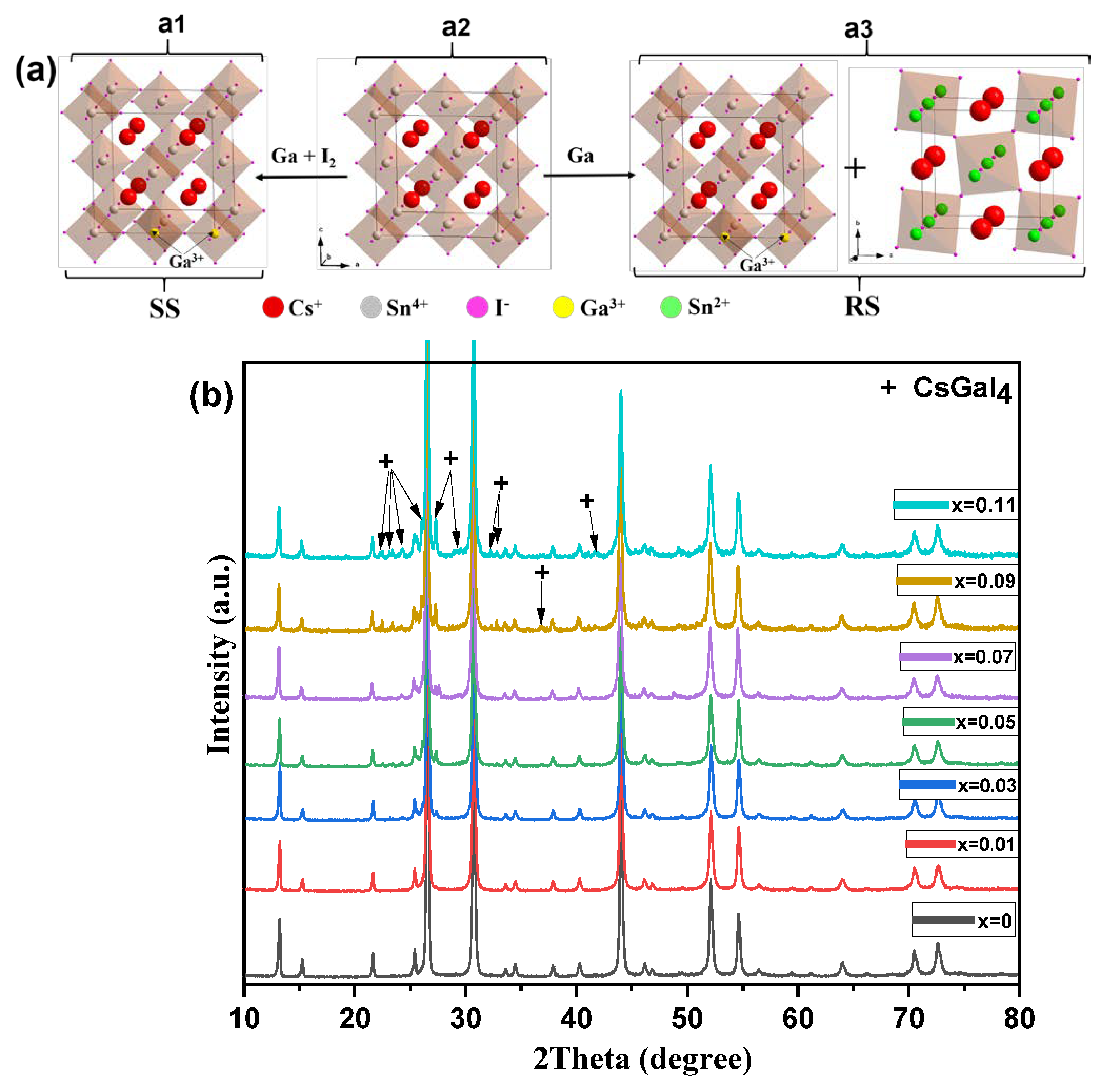
2.1. Materials and Syntheses of RS/SS Compounds
2.2. Characterization Methods
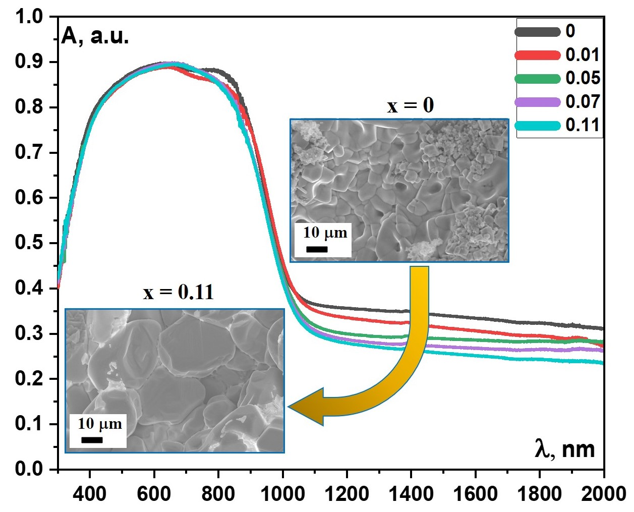
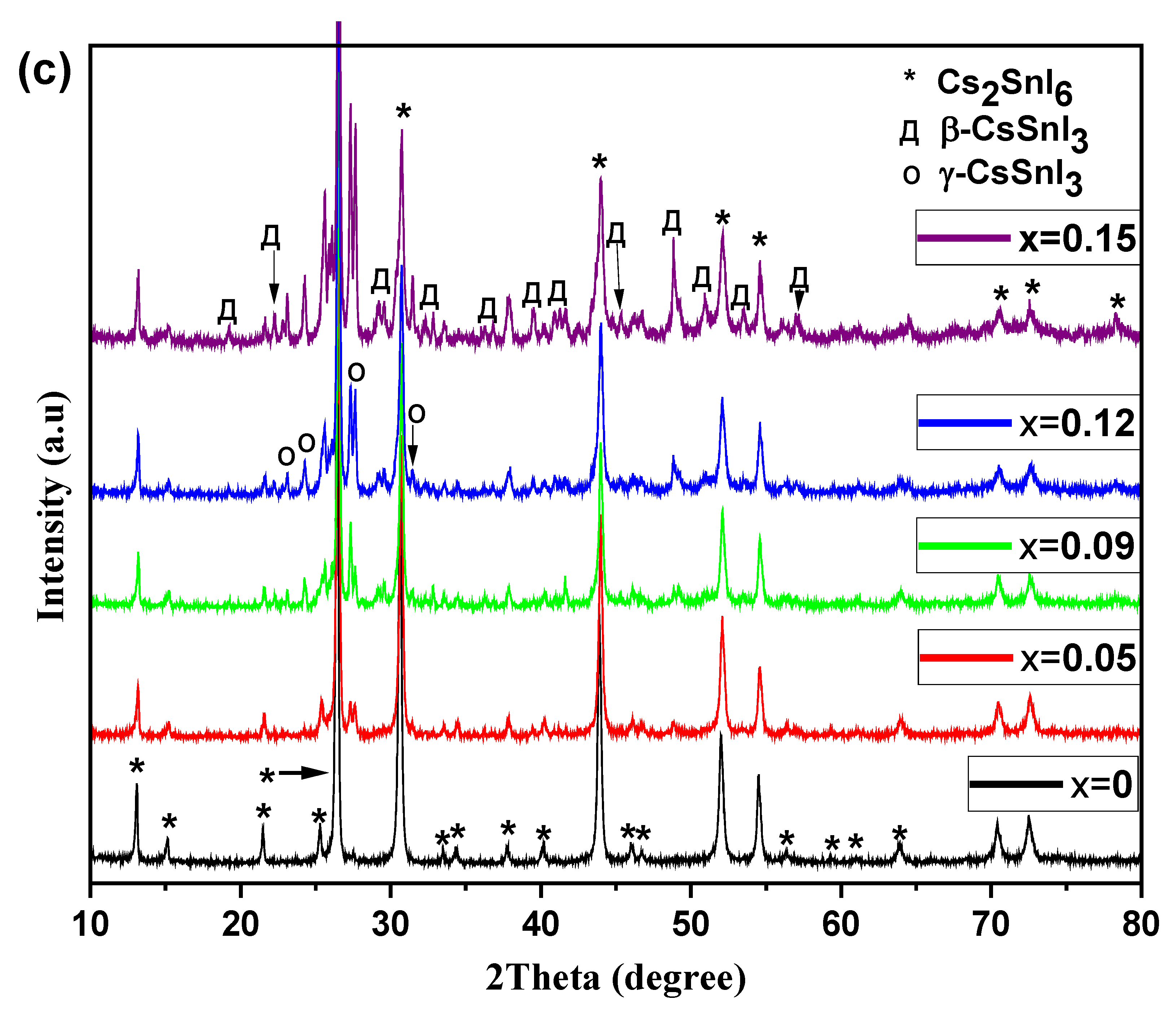
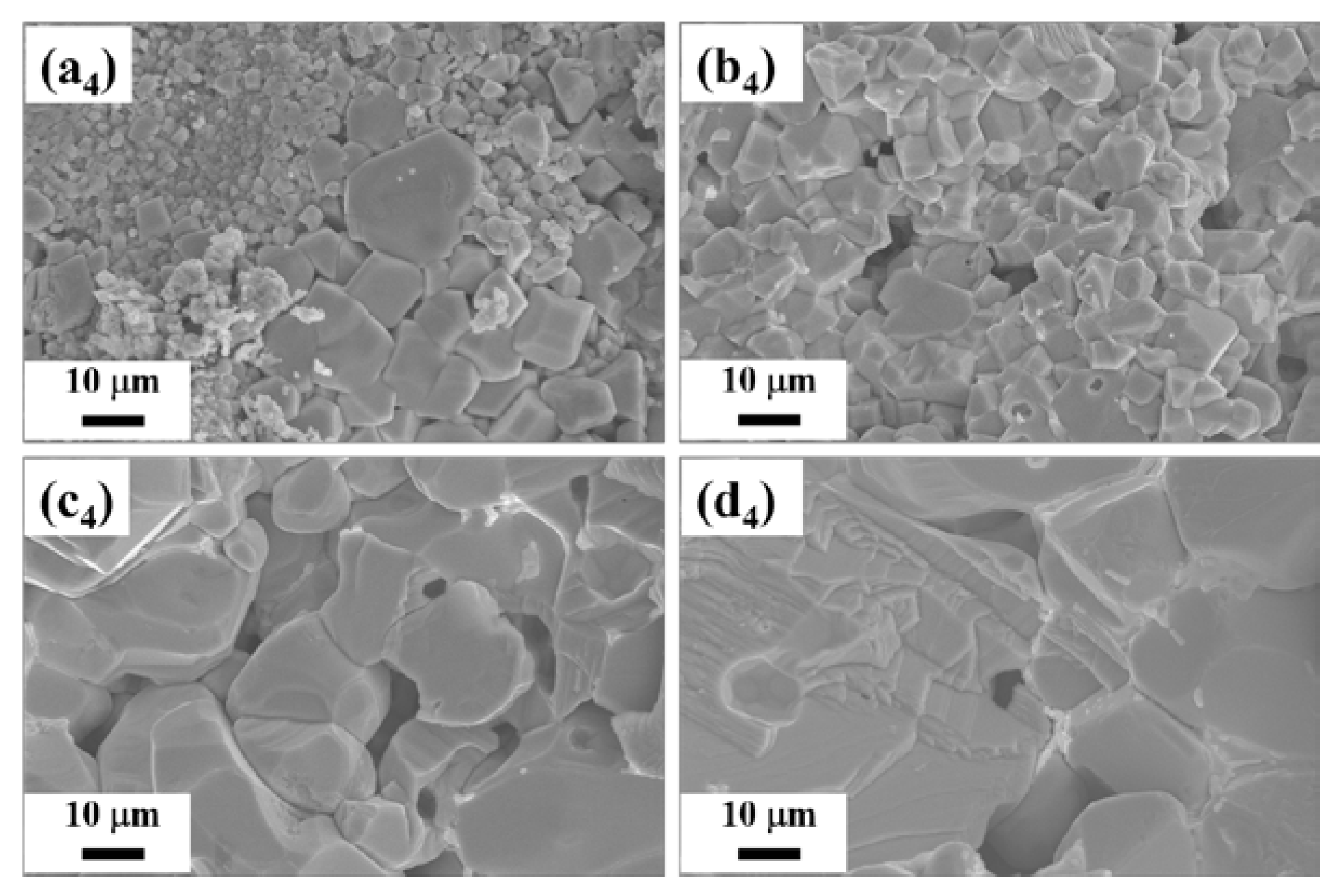
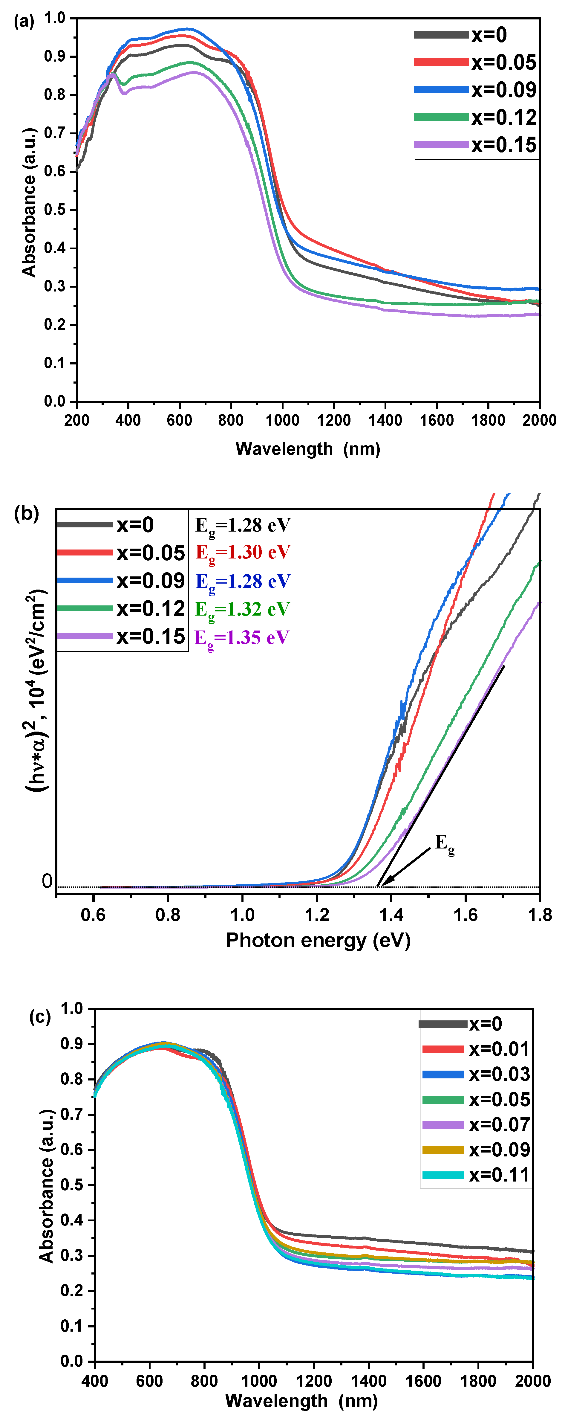
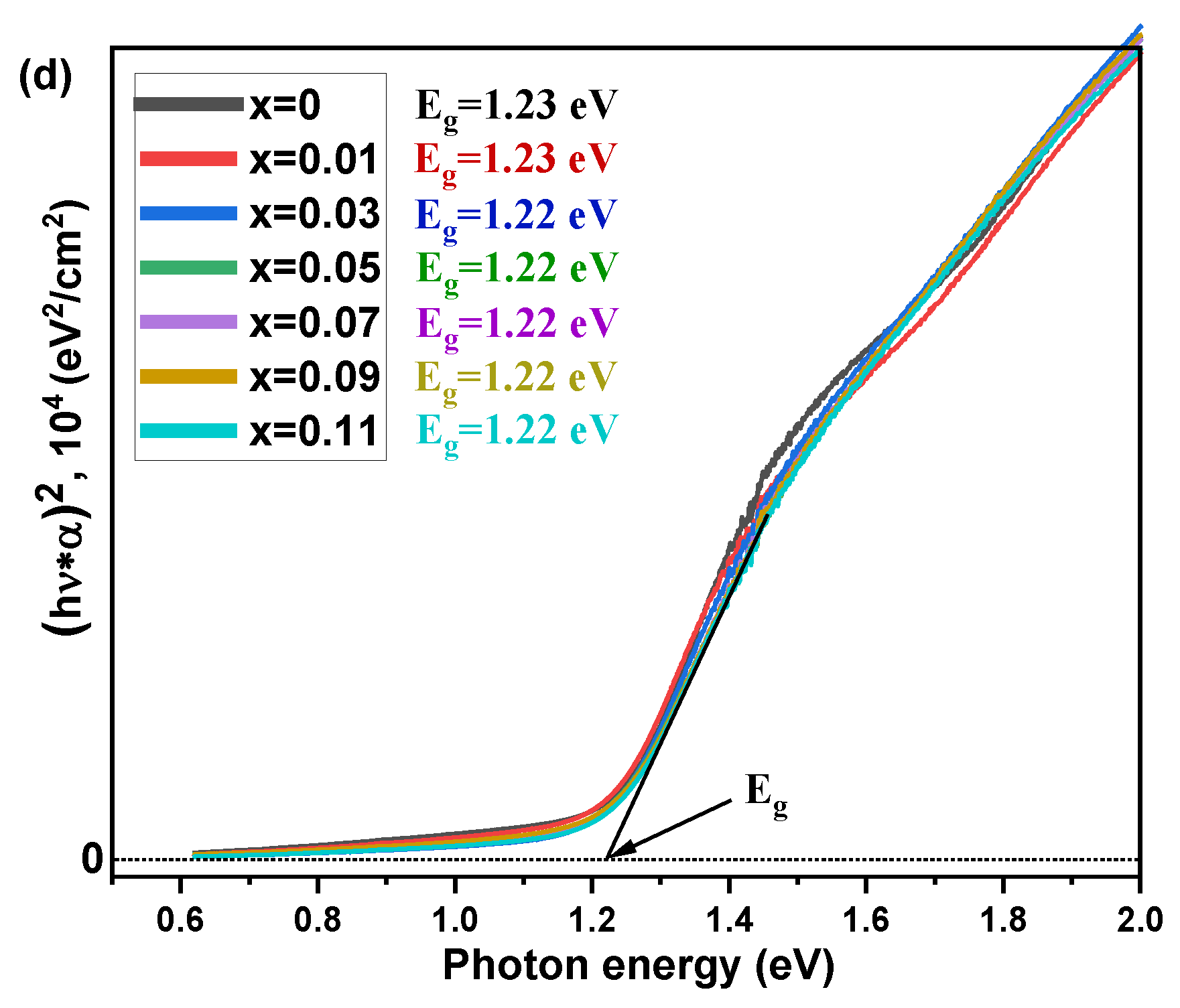
3. Results and Discussion
4. Conclusions
Supplementary Materials
Author Contributions
Funding
Data Availability Statement
Acknowledgments
Conflicts of Interest
References
- Manser, J.S.; Christians, J.A.; Kamat, P.V. Intriguing optoelectronic properties of metal halide perovskites. Chem. Rev. 2016, 116, 12956–13008. [Google Scholar] [CrossRef] [PubMed]
- Mitzi, D.B. Synthesis, structure, and properties of organic-inorganic Perovskites and related materials. Prog. Inorg. Chem. 2007, 48, 1–121. [Google Scholar]
- Min, H.; Lee, D.Y.; Kim, J.; Kim, G.; Lee, K.S.; Kim, J.; Paik, M.J.; Kim, Y.K.; Kim, K.S.; Kim, M.G.; et al. Perovskite solar cells with atomically coherent interlayers on SnO2 electrodes. Nature 2021, 598, 444–450. [Google Scholar] [CrossRef] [PubMed]
- Penconi, M.; Bianchi, G.; Nitti, A.; Savoini, A.; Carbonera, C.; Pasini, D.; Po, R.; Luzzati, S. A donor polymer with a good compromise between efficiency and sustainability for organic solar cells. Adv. Energy Sustain. Res. 2021, 6, 2100069. [Google Scholar] [CrossRef]
- Na, H.-J.; Lee, S.-E.; Lee, E.G.; Lee, J.H.; Gong, Y.J.; Kim, H.; Cho, N.-K.; Kim, Y.S. Nanometer-thick Cs2SnI6 perovskite—Polyethylene glycol dimethacrylate composite films for highly stable broad-band photodetectors. ACS Appl. Nano Mater. 2021, 4, 5309–5318. [Google Scholar] [CrossRef]
- Matthews, P.D.; Lewis, D.J.; O’Brien, P. Updating the road map to metal-halide perovskites for photovoltaics. J. Mater. Chem. A 2017, 5, 17135–17150. [Google Scholar] [CrossRef]
- Green, M.A.; Emery, K.; Hishikawa, Y.; Warta, W.; Dunlop, E.D. Solar cell efficiency tables. Prog. Photovolt. Res. Appl. 2016, 24, 905–913. [Google Scholar] [CrossRef]
- Chung, I.; Lee, B.; He, J.; Chang, R.P.H.; Kanatzidis, M.G. All-solid-state dye-sensitized solar cells with high efficiency. Nature 2012, 485, 486–489. [Google Scholar] [CrossRef]
- Yu, C.; Chen, Z.; Wang, J.J.; Pfenninger, W.; Vockic, N.; Kenney, J.T.; Shum, K. Temperature dependence of the band gap of perovskite semiconductor compound CsSnI3. J. Appl. Phys. 2011, 110, 063526. [Google Scholar] [CrossRef]
- Chen, Z.; Yu, C.; Shum, K.; Wang, J.J.; Pfenninger, W.; Vockic, N.; Midgley, J.; Kenney, J.T. Photoluminescence study of pol-ycrystalline CsSnI3 thin films: Determination of exciton binding energy. J. Lumin. 2012, 132, 345–349. [Google Scholar] [CrossRef]
- Kumar, M.H.; Dharani, S.; Leong, W.L.; Boix, P.P.; Prabhakar, R.R.; Baikie, T.; Shi, C.; Ding, H.; Ramesh, R.; Asta, M.; et al. Lead-free halide perovskite solar cells with high photocurrents realized through vacancy modulation. Adv. Mater. Lett. 2014, 26, 7122–7127. [Google Scholar] [CrossRef] [PubMed]
- Stoumpos, C.C.; Malliakas, C.D.; Kanatzidis, M.G. Semiconducting tin and lead iodide perovskites with organic cations: Phase transitions, high mobilities, and near-infrared photoluminescent properties. Inorg. Chem. 2013, 52, 9019–9038. [Google Scholar] [CrossRef]
- Yamada, K.; Funabiki, S.; Horimoto, H.; Matsui, T.; Okuda, T.; Ichiba, S. Structural phase transitions of the polymorphs of CsSnI3 by means of rietveld analysis of the X-ray diffraction. Chem. Lett. 1991, 20, 801–804. [Google Scholar] [CrossRef]
- Scaife, D.E.; Weller, P.F.; Fisher, W.G. Crystal preparation and properties of cesium tin(II) trihalides. J. Solid State Chem. 1974, 9, 308–314. [Google Scholar] [CrossRef]
- Chung, I.; Song, J.-H.; Im, J.; Androulakis, J.; Malliakas, C.D.; Li, H.; Freeman, A.J.; Kenney, J.T.; Kanatzidis, M.G. CsSnI3: Semiconductor or metal? High electrical conductivity and strong near-infrared photoluminescence from a single material. J. Am. Chem. Soc. 2012, 134, 8579–8587. [Google Scholar] [CrossRef] [PubMed]
- Marshall, K.P.; Walker, M.; Walton, R.I.; Hatton, R.A. Elucidating the role of the hole-extracting electrode on the stability and efficiency of inverted CsSnI3/C60 perovskite photovoltaics. J. Mater. Chem. A 2017, 41, 21836–21845. [Google Scholar] [CrossRef]
- Wijesekara, A.; Varagnolo, S.; Dabera, G.D.M.R.; Marshall, K.P.; Pereira, H.J.; Hatton, R.A. Assessing the suitability of copper thiocyanate as a hole-transport layer in inverted CsSnI3 perovskite photovoltaics. Sci. Rep. 2018, 8, 15722. [Google Scholar] [CrossRef]
- Huang, L.; Lambrecht, W.R.L. Electronic band structure, phonons, and exciton binding energies of halide perovskites CsSnCl3, CsSnBr3, and CsSnI3. Phys. Rev. B 2013, 88, 165203. [Google Scholar] [CrossRef]
- Lora da Silva, E.; Skelton, J.M.; Parker, S.C.; Walsh, A. Phase stability and transformations in the halide perovskite CsSnI3. Phys. Rev. B 2015, 91, 144107. [Google Scholar] [CrossRef]
- Zhang, J.; Yu, C.; Wang, L.; Lili, W.; Ren, Y.; Shum, K. Energy barrier at the N719-dye/CsSnI3 interface for photogenerated holes in dye-sensitized solar cells. Sci. Rep. 2014, 4, 6954. [Google Scholar] [CrossRef]
- Chen, Z.; Wang, J.J.; Ren, Y.; Yu, C.; Shum, K. Schottky solar cells based on CsSnI3 thin-films. Appl. Phys. Lett. 2012, 101, 093901. [Google Scholar] [CrossRef]
- Lee, B.; Stoumpos, C.C.; Zhou, N.; Hao, F.; Malliakas, C.; Yeh, C.-Y.; Marks, T.J.; Kanatzidis, M.G.; Chang, R.P.H. Air-stable molecular semiconducting iodosalts for solar cell applications: Cs2SnI6 as a hole conductor. J. Am. Chem. Soc. 2014, 136, 15379–15385. [Google Scholar] [CrossRef]
- Qiu, X.; Jiang, Y.; Zhang, H.; Qiu, Z.; Yuan, S.; Wang, P.; Cao, B. Lead-free mesoscopic Cs2SnI6perovskite solar cells using different nanostructured ZnO nanorods as electron transport layers. Phys. Status Solidi (RRL) Rapid Res. Lett. 2016, 10, 587–591. [Google Scholar] [CrossRef]
- Chander, N.; Chandrasekhar, P.S.; Komarala, V.K. Solid state plasmonic dye sensitized solar cells based on solution processed perovskite CsSnI3 as the hole transporter. RSC Adv. 2014, 4, 55658–55665. [Google Scholar] [CrossRef]
- Werker, W. Die krystallstruktur des Rb2SnI6 und Cs2SnI6. Recl. Trav. Chim. Pays-Bas 1939, 58, 257–258. [Google Scholar] [CrossRef]
- Kontos, A.G.; Kaltzoglou, A.; Siranidi, E.; Palles, D.; Angeli, G.K.; Arfanis, M.K.; Psycharis, V.; Raptis, Y.S.; Kamitsos, E.I.; Trikalitis, P.N.; et al. Structural stability, vibrational properties, and photolumines-cence in CsSnI3 perovskite upon the addition of SnF2. Inorg. Chem. 2016, 56, 84–91. [Google Scholar] [CrossRef]
- Saparov, B.; Sun, J.; Meng, W.; Xiao, Z.; Duan, H.; Gunawan, O.; Shin, D.; Hill, I.G.; Yan, Y.; Mitzi, D.B. Thin-film deposition and characterization of a Sn-deficient perovskite derivative Cs2SnI6. Chem. Mater. 2016, 28, 2315–2322. [Google Scholar] [CrossRef]
- Xiao, Z.; Lei, H.; Zhang, X.; Zhou, Y.; Hosono, H.; Kamiya, T. Ligand-hole in [SnI6] unit and origin of band gap in photo-voltaic perovskite variant Cs2SnI6. Bull. Chem. Soc. Jpn. 2015, 88, 1250–1255. [Google Scholar] [CrossRef]
- Xiao, Z.; Zhou, Y.; Hosono, H.; Kamiya, T. Intrinsic defects in photovoltaic perovskite variant Cs2SnI6. Phys. Chem. Chem. Phys. 2015, 17, 18900–18903. [Google Scholar] [CrossRef]
- Ju, M.G.; Chen, M.; Zhou, Y.; Garces, H.; Dai, J.; Padture, N.P.; Zeng, X.C. Earth-abundant nontoxic titanium(IV)-based va-cancy-ordered double perovskite halides with tunable 1.0 to 1.8 eV bandgaps for photovoltaic applications. ACS Energy Lett. 2018, 3, 297–304. [Google Scholar] [CrossRef]
- Wang, G.; Wang, D.; Shi, X. Electronic structure and optical properties of Cs2AẊ2X4 (A = Ge, Sn, Pb; Ẋ, X = Cl, Br, I). AIP Adv. 2015, 5, 127224. [Google Scholar] [CrossRef]
- Zhang, P.; Yang, J.; Wei, S.-H. Manipulation of cation combinations and configurations of halide double perovskites for solar cell absorbers. J. Mater. Chem. A 2017, 6, 1809–1815. [Google Scholar] [CrossRef]
- Lee, B.; Krenselewski, A.; Baik, S.I.; Seidman, D.N.; Chang, R.P.H. Solution processing of air-stable molecular semiconducting iodosalts, Cs2SnI6-xBrx, for potential solar cell application. Sustain. Energy Fuels 2017, 1, 710–724. [Google Scholar] [CrossRef]
- Umedov, S.T.; Grigorieva, A.V.; Lepnev, L.S.; Knotko, A.V.; Nakabayashi, K.; Ohkoshi, S.-I.; Shevelkov, A.V. Indium doping of lead-free perovskite Cs2SnI6. Front. Chem. 2020, 8, 564. [Google Scholar] [CrossRef] [PubMed]
- Ke, J.C.R.; Lewis, D.J.; Walton, A.S.; Spencer, B.F.; O’Brien, P.; Thomas, A.G.; Flavell, W.R. Ambient-air-stable inorganic Cs2SnI6 double perovskite thin films via aerosol-assisted chemical vapour deposition. J. Mater. Chem. A 2018, 6, 11205. [Google Scholar] [CrossRef]
- Wu, J.; Zhao, Z.; Zhou, Y. The optoelectronic properties improvement of double perovskites Cs2SnI6 by anionic doping (F−). Sci. Rep. 2022, 12, 935. [Google Scholar] [CrossRef]
- Matsnev, M.E.; Rusakov, V.S. SpectrRelax: An application for mossbauer spectra modeling and fitting. AIP Conf. Proc. 2012, 1489, 178–185. [Google Scholar]
- Matsnev, M.E.; Rusakov, V.S. Study of spatial spin-modulated structures by Mössbauer spectroscopy using SpectrRelax. AIP Conf. Proc. 2014, 1622, 40–49. [Google Scholar] [CrossRef]
- Tudela, D.; Sánchez-Herencia, A.J.; Díaz, M.; Fernández-Ruiz, R.; Menéndez, N.; Tornero, J.D. Mössbauer spectra of tin(IV) iodide complexes. Dalton Trans. 1999, 22, 4019–4023. [Google Scholar] [CrossRef]
- Ullah, S.; Yang, P.; Wang, J.; Liu, L.; Li, Y.; Zafar, Z.; Yang, S.E.; Xia, T.; Guo, H.; Chen, Y. The fabrication of lead-free Cs2SnI6 perovskite films using iodine-rich strategy for optoelectronic applications. Phys. Status Solidi A 2021, 218, 2100271. [Google Scholar] [CrossRef]
- Dalpian, G.M.; Liu, Q.; Stoumpos, C.C.; Douvalis, A.P.; Balasubramanian, M.; Kanatzidis, M.G.; Zunger, A. Changes in charge density vs. changes in formal oxidation states: The case of Sn halide perovskites and their ordered vacancy analogues. Phys. Rev. Mater. 2017, 1, 025401. [Google Scholar] [CrossRef]
- Yamada, K.; Matsui, T.; Tsuritani, T.; Okuda, T.; Ichiba, S. 127I-NQR, 119Sn Mössbauer effect, and electrical conductivity of MSnI3 (M = K, NH4, Rb, Cs, and CH3NH3). Z. Nat. 1990, 45, 307–312. [Google Scholar]
- Qiu, X.; Cao, B.; Yuan, S.; Chen, X.; Qiu, Z.; Jiang, Y.; Ye, Q.; Wang, H.; Zeng, H.; Liu, J.; et al. From unstable CsSnI3 to air-stable Cs2SnI6: A lead-free perovskite solar cell light absorber with bandgap of 1.48 eV and high absorption coefficient. Sol. Energy Mater. Sol. Cells 2017, 159, 227–234. [Google Scholar] [CrossRef]
- Zhang, J.; Li, S.; Yang, P.; Liu, W.; Liao, Y. Enhanced stability of lead-free perovskite heterojunction for photovoltaic applications. J. Mater. Sci. 2018, 53, 4378–4386. [Google Scholar] [CrossRef]


| x | Phase | a, Å | Cell Volume, Å3 | Rp, % | wRp, % | GOF (χ2) |
|---|---|---|---|---|---|---|
| 0 | Cs2SnI6 | 11.6416 (8) | 1577.75 (11) | 7.55 | 10.63 | 1.62 |
| 0.01 | Cs2SnI6 | 11.6418 (9) | 1577.85 (13) | 7.37 | 10.42 | 1.50 |
| 0.03 | Cs2SnI6 | 11.6411 (5) | 1577.58 (7) | 5.59 | 8.69 | 1.31 |
| 0.05 | Cs2SnI6 | 11.6426 (5) | 1578.17 (7) | 6.11 | 9.26 | 1.3 |
| 0.07 | Cs2SnI6 | 11.6411 (3) | 1577.57 (4) | 7.14 | 10.54 | 1.29 |
| 0.09 | Cs2SnI6 | 11.6398 (7) | 1577.04 (9) | 9.48 | 14.14 | 1.19 |
| 0.11 | Cs2SnI6 | 11.6407 (9) | 1577.41 (12) | 9.03 | 13.35 | 1.15 |
| x | Phase | a, Å | Cell Volume, Å3 | Rp, % | wRp, % | GOF (χ2) |
|---|---|---|---|---|---|---|
| 0 | Cs2SnI6 | 11.6458 (9) | 1579.450 (13) | 9.3 | 13.19 | 1.25 |
| 0.05 | Cs2SnI6 | 11.6438 (3) | 1578.654 (2) | 9.8 | 14.17 | 1.17 |
| CsSnI3 | 8.7252 (1) | 477.137 (7) | ||||
| 0.09 | Cs2SnI6 | 11.6482 (1) | 1580.43 (2) | 10.16 | 14.8 | 1.22 |
| CsSnI3 | 8.7339 (8) | 477.29 (6) | ||||
| 0.12 | Cs2SnI6 | 11.647 (1) | 1580.26 (2) | 10.64 | 15.01 | 1.20 |
| CsSnI3 | 8.6995 (2) | 482.23 (8) | ||||
| 0.15 | Cs2SnI6 | 11.664 (2) | 1587.18 (2) | 11.81 | 16.43 | 1.27 |
| CsSnI3 | 8.6016 (2) | 461.24 (10) |
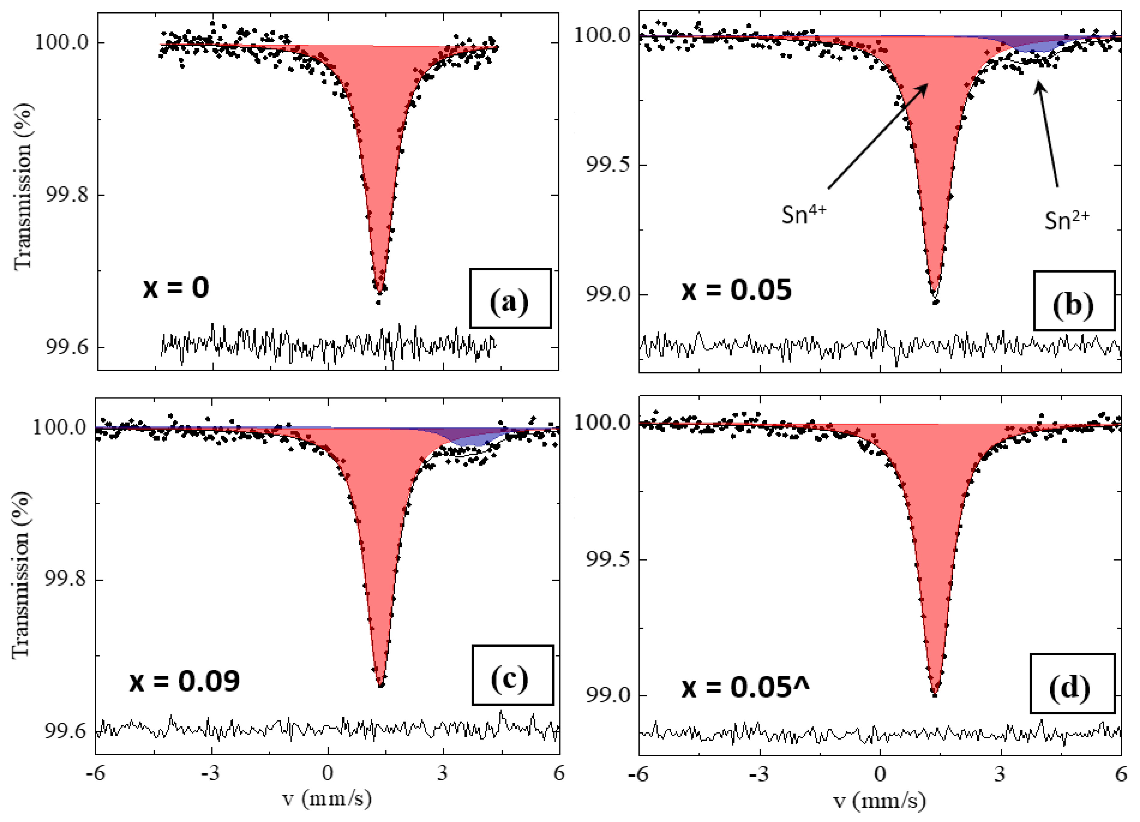
| Series | x | Tin Type | δ (mm/s) | ∆ (mm/s) | W (mm/s) | A (%) |
|---|---|---|---|---|---|---|
| RS | 0.00 | Sn4+ | 1.36 (1) | 0.15 (4) | 0.85 * | 100 |
| 0.05 | Sn4+ | 1.35 (1) | 0.18 (3) | 0.85 * | 91.4 (9) | |
| Sn2+ | 3.84 (8) | 0.31 (7) | 0.85 * | 8.6 (9) | ||
| 0.09 | Sn4+ | 1.36 (1) | 0.17 (3) | 0.85 * | 90.9 (7) | |
| Sn2+ | 3.72 (7) | 0.30 (6) | 0.85 * | 9.1 (7) | ||
| SS | 0.05^ | Sn4+ | 1.37 (1) | 0.22 (2) | 0.85 * | 100 |
Disclaimer/Publisher’s Note: The statements, opinions and data contained in all publications are solely those of the individual author(s) and contributor(s) and not of MDPI and/or the editor(s). MDPI and/or the editor(s) disclaim responsibility for any injury to people or property resulting from any ideas, methods, instructions or products referred to in the content. |
© 2023 by the authors. Licensee MDPI, Basel, Switzerland. This article is an open access article distributed under the terms and conditions of the Creative Commons Attribution (CC BY) license (https://creativecommons.org/licenses/by/4.0/).
Share and Cite
Umedov, S.T.; Grigorieva, A.V.; Sobolev, A.V.; Knotko, A.V.; Lepnev, L.S.; Kolesnikov, E.A.; Charkin, D.O.; Shevelkov, A.V. Controlled Reduction of Sn4+ in the Complex Iodide Cs2SnI6 with Metallic Gallium. Nanomaterials 2023, 13, 427. https://doi.org/10.3390/nano13030427
Umedov ST, Grigorieva AV, Sobolev AV, Knotko AV, Lepnev LS, Kolesnikov EA, Charkin DO, Shevelkov AV. Controlled Reduction of Sn4+ in the Complex Iodide Cs2SnI6 with Metallic Gallium. Nanomaterials. 2023; 13(3):427. https://doi.org/10.3390/nano13030427
Chicago/Turabian StyleUmedov, Shodruz T., Anastasia V. Grigorieva, Alexey V. Sobolev, Alexander V. Knotko, Leonid S. Lepnev, Efim A. Kolesnikov, Dmitri O. Charkin, and Andrei V. Shevelkov. 2023. "Controlled Reduction of Sn4+ in the Complex Iodide Cs2SnI6 with Metallic Gallium" Nanomaterials 13, no. 3: 427. https://doi.org/10.3390/nano13030427
APA StyleUmedov, S. T., Grigorieva, A. V., Sobolev, A. V., Knotko, A. V., Lepnev, L. S., Kolesnikov, E. A., Charkin, D. O., & Shevelkov, A. V. (2023). Controlled Reduction of Sn4+ in the Complex Iodide Cs2SnI6 with Metallic Gallium. Nanomaterials, 13(3), 427. https://doi.org/10.3390/nano13030427