
A Strategy for Tuning Electron–Phonon Coupling and Carrier Cooling in Lead Halide Perovskite Nanocrystals


Abstract
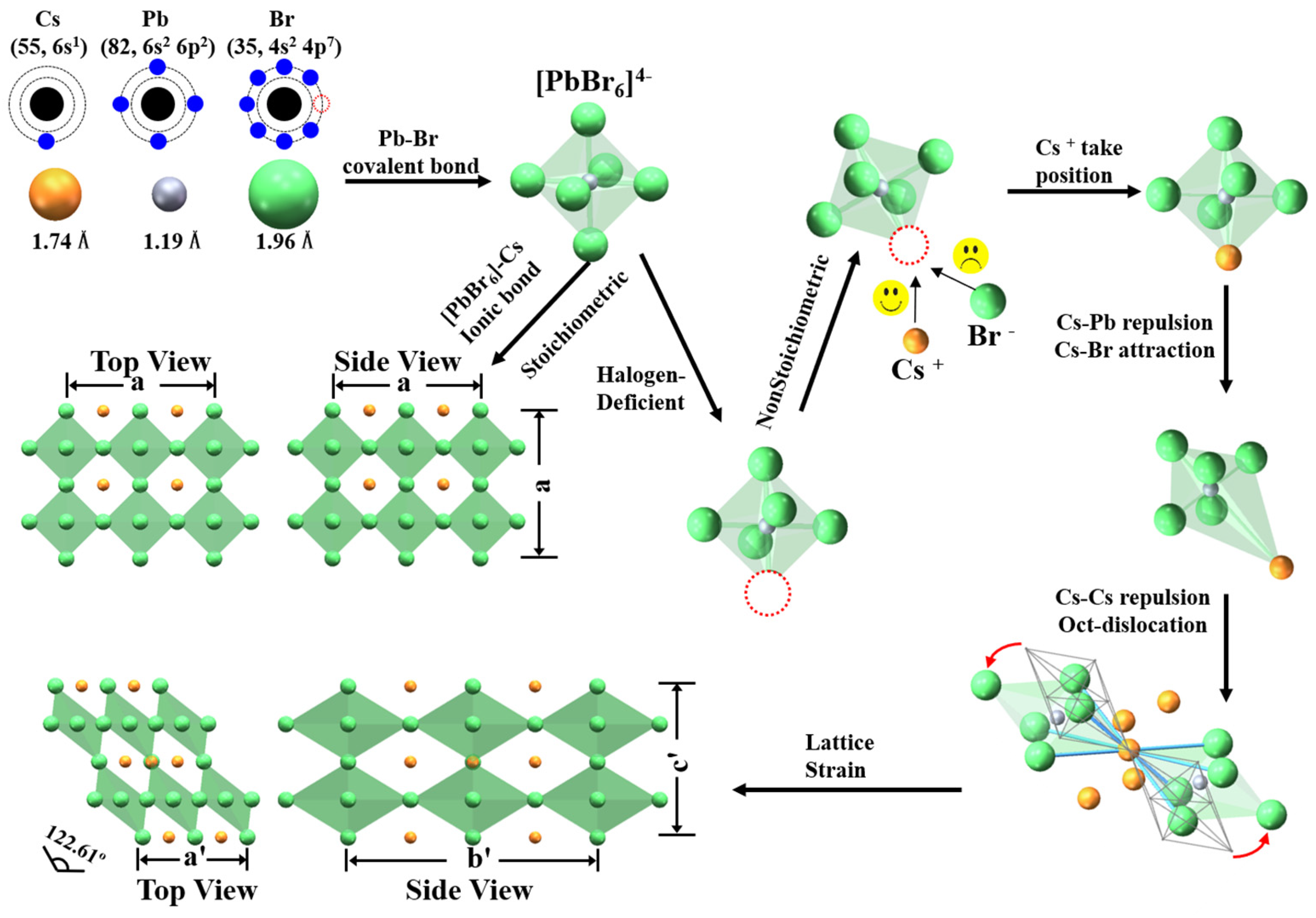
:1. Introduction
2. Materials and Methods
2.1. Materials
2.2. Synthesis
2.3. Characterization
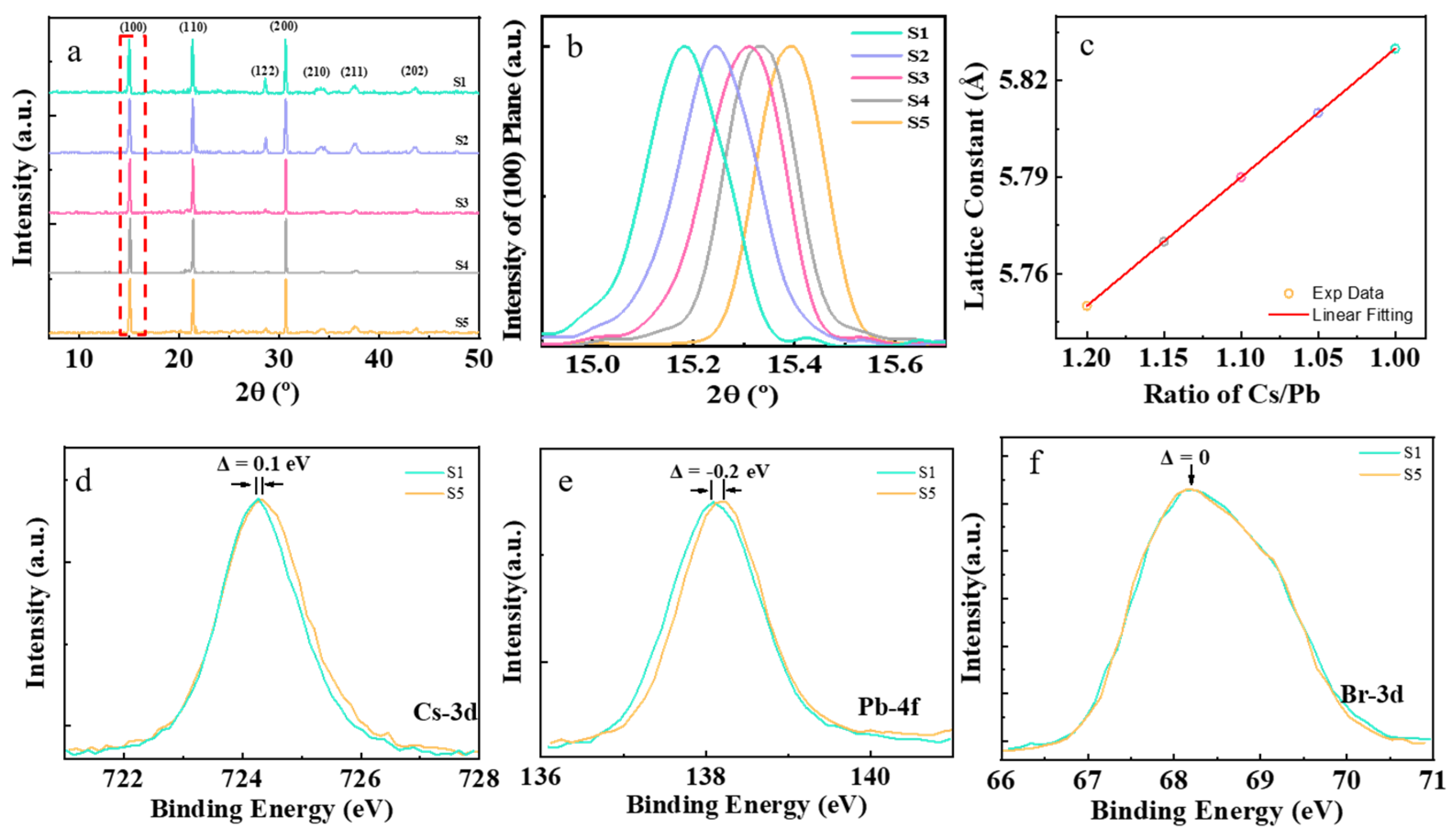
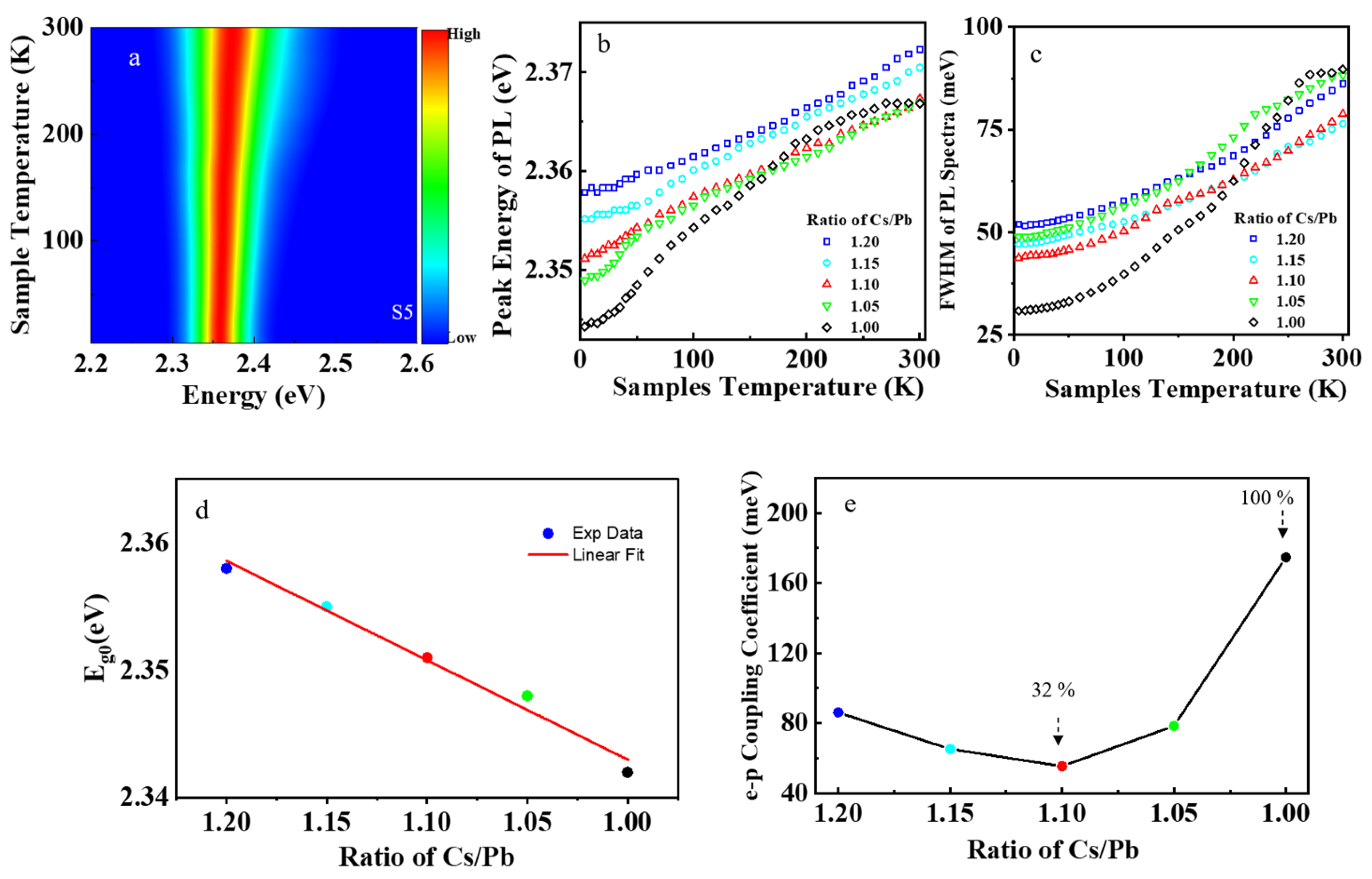
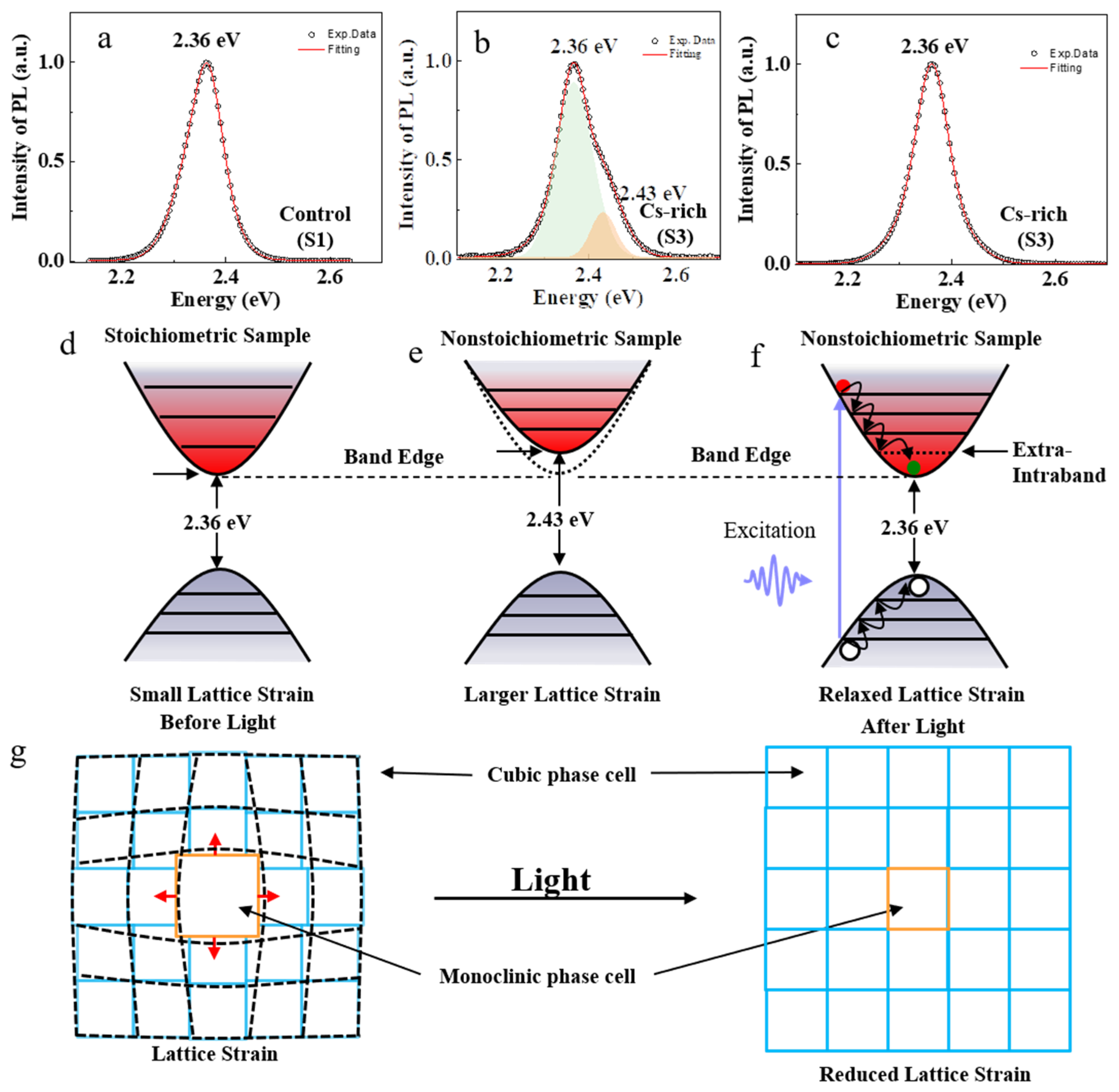
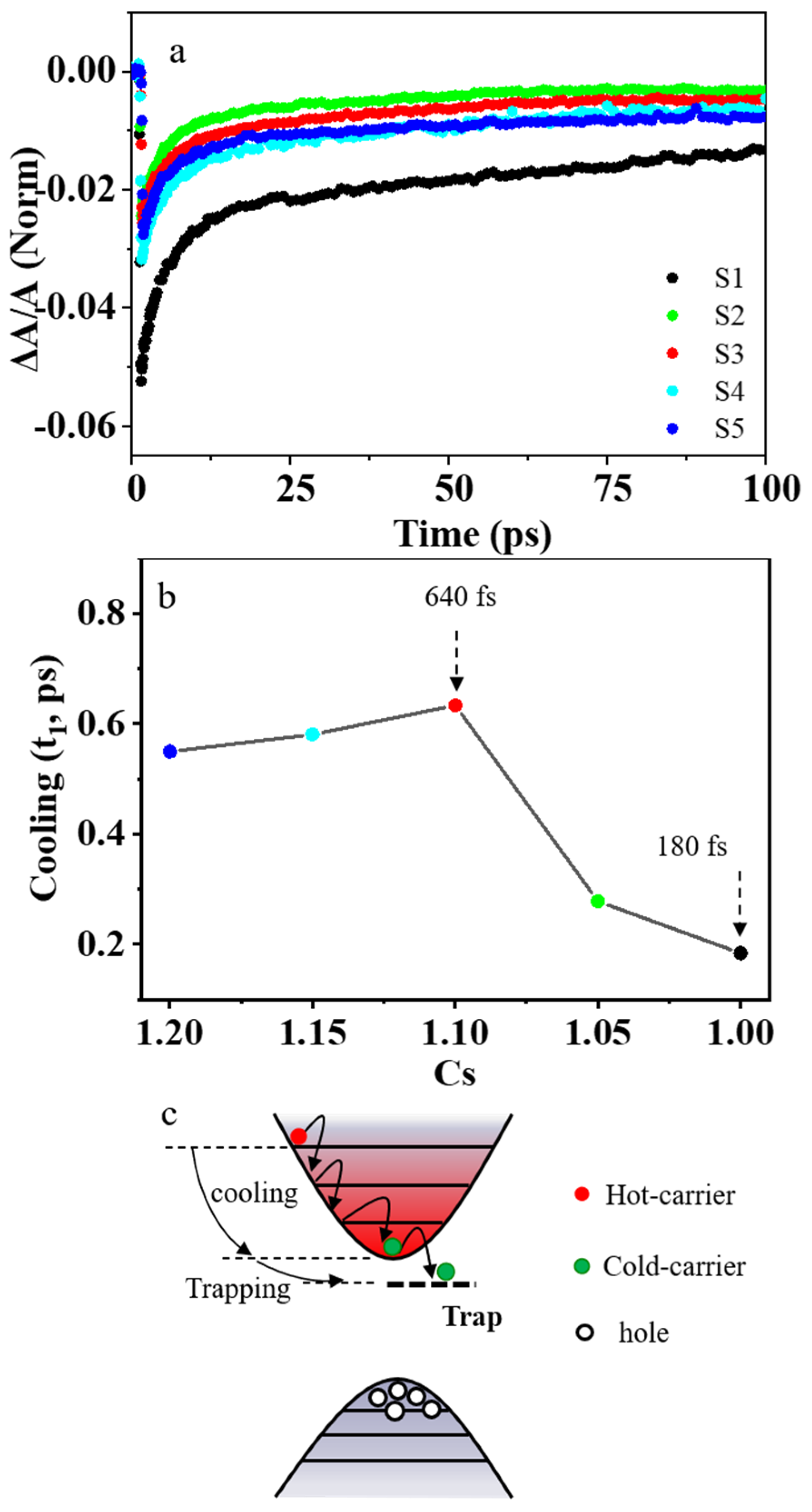
3. Results and Discussion
4. Conclusions
Supplementary Materials
Author Contributions
Funding
Data Availability Statement
Acknowledgments
Conflicts of Interest
References
- Chen, S.; Dai, X.; Xu, S.; Jiao, H.; Zhao, L.; Huang, J. Stabilizing perovskite-substrate interfaces for high-performance perovskite modules. Science 2021, 373, 902–907. [Google Scholar] [CrossRef] [PubMed]
- Tsai, H.; Shrestha, S.; Vilá, R.A.; Huang, W.; Liu, C.; Hou, C.-H.; Huang, H.-H.; Wen, X.; Li, M.; Wiederrecht, G.; et al. Bright and stable light-emitting diodes made with perovskite nanocrystals stabilized in metal–organic frameworks. Nat. Photonics 2021, 15, 843–849. [Google Scholar] [CrossRef]
- Feng, J.G.; Gong, C.; Gao, H.F.; Wen, W.; Gong, Y.J.; Jiang, X.Y.; Zhang, B.; Wu, Y.C.; Wu, Y.S.; Fu, H.B.; et al. Single-crystalline layered metal-halide perovskite nanowires for ultrasensitive photodetectors. Nat. Electron. 2018, 1, 404–410. [Google Scholar] [CrossRef]
- Jacak, J.E.; Jacak, W.A. Routes for metallization of perovskite solar cells. Materials 2022, 15, 2254. [Google Scholar] [CrossRef] [PubMed]
- Protesescu, L.; Yakunin, S.; Bodnarchuk, M.I.; Krieg, F.; Caputo, R.; Hendon, C.H.; Yang, R.X.; Walsh, A.; Kovalenko, M.V. Nanocrystals of Cesium Lead Halide Perovskites (CsPbX3, X = Cl, Br, and I): Novel Optoelectronic Materials Showing Bright Emission with Wide Color Gamut. Nano Lett. 2015, 15, 3692–3696. [Google Scholar] [CrossRef] [PubMed]
- Gautier, R.; Paris, M.; Massuyeau, F. Exciton Self-Trapping in Hybrid Lead Halides: Role of Halogen. J. Am. Chem. Soc. 2019, 141, 12619–12623. [Google Scholar] [CrossRef] [PubMed]
- An, L.C.; Li, K.; Li, Z.G.; Zhu, S.; Li, Q.; Zhang, Z.Z.; Ji, L.J.; Li, W.; Bu, X.H. Engineering Elastic Properties of Isostructural Molecular Perovskite Ferroelectrics via B-Site Substitution. Small 2021, 17, 2006021. [Google Scholar] [CrossRef]
- Hao, F.; Stoumpos, C.C.; Cao, D.H.; Chang, R.P.H.; Kanatzidis, M.G. Lead-free solid-state organic–inorganic halide perovskite solar cells. Nat. Photonics 2014, 8, 489–494. [Google Scholar] [CrossRef]
- Zheng, X.; Chen, B.; Dai, J.; Fang, Y.; Bai, Y.; Lin, Y.; Wei, H.; Zeng, X.C.; Huang, J. Defect passivation in hybrid perovskite solar cells using quaternary ammonium halide anions and cations. Nat. Energy 2017, 2, 17102. [Google Scholar] [CrossRef]
- Zhang, S.; Wu, S.; Chen, R.; Chen, W.; Huang, Y.; Zhu, H.; Yang, Z.; Chen, W. Controlling Orientation Diversity of Mixed Ion Perovskites: Reduced Crystal Microstrain and Improved Structural Stability. J. Phys. Chem. Lett. 2019, 10, 2898–2903. [Google Scholar] [CrossRef]
- Chen, L.; Tan, Y.Y.; Chen, Z.X.; Wang, T.; Hu, S.; Nan, Z.A.; Xie, L.Q.; Hui, Y.; Huang, J.X.; Zhan, C.; et al. Toward Long-Term Stability: Single-Crystal Alloys of Cesium-Containing Mixed Cation and Mixed Halide Perovskite. J. Am. Chem. Soc. 2019, 141, 1665–1671. [Google Scholar] [CrossRef] [PubMed]
- Correa-Baena, J.P.; Luo, Y.; Brenner, T.M.; Snaider, J.; Sun, S.; Li, X.; Jensen, M.A.; Hartono, N.T.P.; Nienhaus, L.; Wieghold, S.; et al. Homogenized halides and alkali cation segregation in alloyed organic-inorganic perovskites. Science 2019, 363, 627–631. [Google Scholar] [CrossRef] [PubMed]
- Qiao, L.; Fang, W.H.; Long, R.; Prezhdo, O.V. Extending Carrier Lifetimes in Lead Halide Perovskites with Alkali Metals by Passivating and Eliminating Halide Interstitial Defects. Angew. Chem.-Int. Edit. 2020, 59, 4684–4690. [Google Scholar] [CrossRef] [PubMed]
- Kausar, A.; Sattar, A.; Xu, C.; Zhang, S.; Kang, Z.; Zhang, Y. Advent of alkali metal doping: A roadmap for the evolution of perovskite solar cells. Chem. Soc. Rev. 2021, 50, 2696–2736. [Google Scholar] [CrossRef] [PubMed]
- Chen, Y.; Li, N.; Wang, L.; Li, L.; Xu, Z.; Jiao, H.; Liu, P.; Zhu, C.; Zai, H.; Sun, M.; et al. Impacts of alkaline on the defects property and crystallization kinetics in perovskite solar cells. Nat. Commun. 2019, 10, 1112. [Google Scholar] [CrossRef] [PubMed]
- Uchida, R.; Binet, S.; Arora, N.; Jacopin, G.; Alotaibi, M.H.; Taubert, A.; Zakeeruddin, S.M.; Dar, M.I.; Graetzel, M. Insights about the Absence of Rb Cation from the 3D Perovskite Lattice: Effect on the Structural, Morphological, and Photophysical Properties and Photovoltaic Performance. Small 2018, 14, 1802033. [Google Scholar] [CrossRef] [PubMed]
- Hu, Y.; Hutter, E.M.; Rieder, P.; Grill, I.; Hanisch, J.; Aygüler, M.F.; Hufnagel, A.G.; Handloser, M.; Bein, T.; Hartschuh, A.; et al. Understanding the Role of Cesium and Rubidium Additives in Perovskite Solar Cells: Trap States, Charge Transport, and Recombination. Adv. Energy Mater. 2018, 8, 1703057. [Google Scholar] [CrossRef]
- Abdi-Jalebi, M.; Andaji-Garmaroudi, Z.; Cacovich, S.; Stavrakas, C.; Philippe, B.; Richter, J.M.; Alsari, M.; Booker, E.P.; Hutter, E.M.; Pearson, A.J.; et al. Maximizing and Stabilizing Luminescence from Halide Perovskites with Potassium Passivation. Nature 2018, 555, 497–501. [Google Scholar] [CrossRef]
- Chen, W.; Zhou, Y.; Chen, G.; Wu, Y.; Tu, B.; Liu, F.Z.; Huang, L.; Ng, A.M.C.; Djurišić, A.B.; He, Z. Alkali Chlorides for the Suppression of the Interfacial Recombination in Inverted Planar Perovskite Solar Cells. Adv. Energy Mater. 2019, 9, 1803872. [Google Scholar] [CrossRef]
- Zhao, W.; Yao, Z.; Yu, F.; Yang, D.; Liu, S.F. Alkali Metal Doping for Improved CH3NH3PbI3 Perovskite Solar Cells. Adv. Sci. 2018, 5, 1700131. [Google Scholar] [CrossRef]
- Liu, F.; Jiang, J.; Zhang, Y.; Ding, C.; Toyoda, T.; Hayase, S.; Wang, R.; Tao, S.; Shen, Q. Near-Infrared Emission from Tin-Lead (Sn-Pb) Alloyed Perovskite Quantum Dots by Sodium Doping. Angew. Chem.-Int. Edit. 2020, 59, 8421–8424. [Google Scholar] [CrossRef] [PubMed]
- Fang, Z.; He, H.; Gan, L.; Li, J.; Ye, Z. Understanding the Role of Lithium Doping in Reducing Nonradiative Loss in Lead Halide Perovskites. Adv. Sci. 2018, 5, 1800736. [Google Scholar] [CrossRef] [PubMed]
- Li, M.; Fu, J.; Xu, Q.; Sum, T.C. Slow Hot-Carrier Cooling in Halide Perovskites: Prospects for Hot-Carrier Solar Cells. Adv. Mater. 2019, 31, 1802486. [Google Scholar] [CrossRef] [PubMed]
- Price, M.B.; Butkus, J.; Jellicoe, T.C.; Sadhanala, A.; Briane, A.; Halpert, J.E.; Broch, K.; Hodgkiss, J.M.; Friend, R.H.; Deschler, F. Hot-carrier cooling and photoinduced refractive index changes in organic–inorganic lead halide perovskites. Nat. Commun. 2015, 6, 8420. [Google Scholar] [CrossRef] [PubMed]
- Richter, J.M.; Branchi, F.; Camargo, F.V.d.A.; Zhao, B.; Friend, R.H.; Cerullo, G.; Deschler, F. Ultrafast carrier thermalization in lead iodide perovskite probed with two-dimensional electronic spectroscopy. Nat. Commun. 2017, 8, 376. [Google Scholar] [CrossRef] [PubMed]
- Kawai, H.; Giorgi, G.; Marini, A.; Yamashita, K. The mechanism of slow hot-hole cooling in lead-iodide perovskite: First-principles calculation on carrier lifetime from electron–phonon interaction. Nano Lett. 2015, 15, 3103. [Google Scholar] [CrossRef] [PubMed]
- Wright, A.; Verdi, C.; Milot, R.; Eperon, G.; Pérez-Osorio, M.; Snaith, H.; Giustino, F.; Johnston, M.; Herz, L. Electron–phonon coupling in hybrid lead halide perovskites. Nat. Commun. 2016, 7, 11755. [Google Scholar] [CrossRef] [PubMed]
- Huang, X.; Li, X.; Tao, Y.; Guo, S.; Gu, J.; Hong, H.; Yao, Y.; Guan, Y.; Gao, Y.; Li, C.; et al. Understanding electron–phonon interactions in 3D lead halide perovskites from the stereochemical expression of 6s2 lone pairs. J. Am. Chem. Soc. 2022, 144, 12247–12260. [Google Scholar] [CrossRef]
- Pope, C.G. X-Ray Diffraction and the Bragg Equation. J. Chem. Educ. 1997, 74, 129–131. [Google Scholar] [CrossRef]
- Zhao, Y.; Wang, Q.; Teng, Y.; Xin, Z.; Cao, Y.; Duan, J.; Guo, Q.; Wang, Y.; Tang, Q. Strain management in perovskite solar cells. Energy Lab. 2023, 1, 230004. [Google Scholar] [CrossRef]
- Chang, J.; Lin, Z.; Zhu, H.; Isikgor, F.H.; Xu, Q.-H.; Zhang, C.; Hao, Y.; Ouyang, J. Enhancing the photovoltaic performance of planar heterojunction perovskite solar cells by doping the perovskite layer with alkali metal ions. J. Mater. Chem. A 2016, 4, 16546–16552. [Google Scholar] [CrossRef]
- Li, X.; Wu, Y.; Zhang, S.; Cai, B.; Gu, Y.; Song, J.; Zeng, H. CsPbX3 Quantum Dots for Lighting and Displays: Room-Temperature Synthesis, Photoluminescence Superiorities, Underlying Origins and White Light-Emitting Diodes. Adv. Funct. Mater. 2016, 26, 2435–2445. [Google Scholar] [CrossRef]
- Doherty, T.A.S.; Winchester, A.J.; Macpherson, S.; Johnstone, D.N.; Pareek, V.; Tennyson, E.M.; Kosar, S.; Kosasih, F.U.; Anaya, M.; Abdi-Jalebi, M.; et al. Performance-limiting nanoscale trap clusters at grain junctions in halide perovskites. Nature 2020, 580, 360–366. [Google Scholar] [CrossRef] [PubMed]
- Yang, W.S.; Park, B.W.; Jung, E.H.; Jeon, N.J.; Kim, Y.C.; Lee, D.U.; Shin, S.S.; Seo, J.; Kim, E.K.; Noh, J.H.; et al. Iodide management in formamidinium-lead-halide-based perovskite layers for efficient solar cells. Science 2017, 356, 1376–1379. [Google Scholar] [CrossRef] [PubMed]
- Shi, H.; Zhang, X.; Sun, X.; Zhang, X. Strong hot-phonon bottleneck effect in all-inorganic perovskite nanocrystals. Appl. Phys. Lett. 2020, 116, 151902. [Google Scholar] [CrossRef]
- Rolston, N.; Bush, K.A.; Printz, A.D.; Gold-Parker, A.; Ding, Y.; Toney, M.F.; McGehee, M.D.; Dauskardt, R.H. Engineering Stress in Perovskite Solar Cells to Improve Stability. Adv. Energy Mater. 2018, 8, 1802139. [Google Scholar] [CrossRef]
- Zhu, C.; Niu, X.; Fu, Y.; Li, N.; Hu, C.; Chen, Y.; He, X.; Na, G.; Liu, P.; Zai, H.; et al. Strain engineering in perovskite solar cells and its impacts on carrier dynamics. Nat. Commun. 2019, 10, 815. [Google Scholar] [CrossRef]
- Prasanna, R.; Gold-Parker, A.; Leijtens, T.; Conings, B.; Babayigit, A.; Boyen, H.G.; Toney, M.F.; McGehee, M.D. Band Gap Tuning via Lattice Contraction and Octahedral Tilting in Perovskite Materials for Photovoltaics. J. Am. Chem. Soc. 2017, 139, 11117–11124. [Google Scholar] [CrossRef]
- Al-Ashouri, A.; Kohnen, E.; Li, B.; Magomedov, A.; Hempel, H.; Caprioglio, P.; Marquez, J.A.; Morales Vilches, A.B.; Kasparavicius, E.; Smith, J.A.; et al. Monolithic perovskite/silicon tandem solar cell with >29% efficiency by enhanced hole extraction. Science 2020, 370, 1300–1309. [Google Scholar] [CrossRef]
- Shi, H.; Zhang, X.; Sun, X.; Chen, R.; Zhang, X. Direct and Indirect Recombination and Thermal Kinetics of Excitons in Colloidal All-Inorganic Lead Halide Perovskite Nanocrystals. J. Phys. Chem. C 2019, 123, 19844–19850. [Google Scholar] [CrossRef]
- Chu, W.; Saidi, W.A.; Zhao, J.; Prezhdo, O.V. Soft Lattice and Defect Covalency Rationalize Tolerance of β-CsPbI3 Perovskite Solar Cells to Native Defects. Angew. Chem.-Int. Edit. 2020, 59, 6435–6441. [Google Scholar] [CrossRef] [PubMed]
- Zhou, Y.; You, L.; Wang, S.; Ku, Z.; Fan, H.; Schmidt, D.; Rusydi, A.; Chang, L.; Wang, L.; Ren, P.; et al. Giant photostriction in organic-inorganic lead halide perovskites. Nat. Commun. 2016, 7, 11193. [Google Scholar] [CrossRef] [PubMed]
- Kundys, B. Photostrictive materials. Appl. Phys. Rev. 2015, 2, 011301. [Google Scholar] [CrossRef]
- Wei, H.; Yang, Y.; Chen, S.; Xiang, H.J. Lead-free hybrid perovskite N(CH3)4SnI3 with robust ferroelectricity induced by large and non-polar N(CH3)4+ molecular cation. Nat. Commun. 2021, 12, 637. [Google Scholar] [CrossRef]
- Tsai, H.; Asadpour, R.; Blancon, J.C.; Stoumpos, C.C.; Durand, O.; Strzalka, J.W.; Chen, B.; Verduzco, R.; Ajayan, P.M.; Tretiak, S.; et al. Light-induced lattice expansion leads to high-efficiency perovskite solar cells. Science 2018, 360, 67–70. [Google Scholar] [CrossRef]
- Wu, X.; Tan, L.Z.; Shen, X.; Hu, T.; Miyata, K.; Trinh, M.T.; Li, R.; Coffee, R.; Liu, S.; Egger, D.A.; et al. Light-induced picosecond rotational disordering of the inorganic sublattice in hybrid perovskites. Sci. Adv. 2017, 3, e1602388. [Google Scholar] [CrossRef]
- Cho, Y.; Kim, H.; Lee, S.; Lee, E.; Hwang, Y.; Kim, H.; Seo, S.; Tran, N.; Kim, W.; Jung, H.; et al. Inductive effect of Lewis acidic dopants on the band levels of perovskite for a photocatalytic reaction. ACS Appl. Mater. Interfaces 2022, 14, 53603–53614. [Google Scholar] [CrossRef]
- Li, F.; Zhou, S.; Yuan, J.; Qin, C.; Yang, Y.; Shi, J.; Ling, X.; Li, Y.; Ma, W. Perovskite Quantum Dot Solar Cells with 15.6% Efficiency and Improved Stability Enabled by an α-CsPbI3/FAPbI3 Bilayer Structure. ACS Energy Lett. 2019, 4, 2571–2578. [Google Scholar] [CrossRef]
- Yao, J.S.; Ge, J.; Han, B.N.; Wang, K.H.; Yao, H.B.; Yu, H.L.; Li, J.H.; Zhu, B.S.; Song, J.Z.; Chen, C.; et al. Ce3+-Doping to Modulate Photoluminescence Kinetics for Efficient CsPbBr3 Nanocrystals Based Light-Emitting Diodes. J. Am. Chem. Soc. 2018, 140, 3626–3634. [Google Scholar] [CrossRef]
- Chung, H.; Jung, S.I.; Kim, H.J.; Cha, W.; Sim, E.; Kim, D.; Koh, W.K.; Kim, J. Composition-Dependent Hot Carrier Relaxation Dynamics in Cesium Lead Halide (CsPbX3, X = Br and I) Perovskite Nanocrystals. Angew. Chem.-Int. Edit. 2017, 56, 4160–4164. [Google Scholar] [CrossRef]
- Wang, R.; Xue, J.; Wang, K.L.; Wang, Z.K.; Luo, Y.; Fenning, D.; Xu, G.; Nuryyeva, S.; Huang, T.; Zhao, Y.; et al. Constructive molecular configurations for surface-defect passivation of perovskite photovoltaics. Science 2019, 366, 1509–1513. [Google Scholar] [CrossRef] [PubMed]


| Samples | S1 | S2 | S3 | S4 | S5 |
|---|---|---|---|---|---|
| CsBr (mg) | 85.10 | 89.36 | 93.61 | 97.87 | 102.12 |
| PbBr2 (mg) | 146.70 | 146.70 | 146.70 | 146.70 | 146.70 |
| Cs:Pb | 1.00:1 | 1.05:1 | 1.10:1 | 1.15:1 | 1.20:1 |
Disclaimer/Publisher’s Note: The statements, opinions and data contained in all publications are solely those of the individual author(s) and contributor(s) and not of MDPI and/or the editor(s). MDPI and/or the editor(s) disclaim responsibility for any injury to people or property resulting from any ideas, methods, instructions or products referred to in the content. |
© 2023 by the authors. Licensee MDPI, Basel, Switzerland. This article is an open access article distributed under the terms and conditions of the Creative Commons Attribution (CC BY) license (https://creativecommons.org/licenses/by/4.0/).
Share and Cite
Shi, H.; Zhang, X.; Li, R.; Zhang, X. A Strategy for Tuning Electron–Phonon Coupling and Carrier Cooling in Lead Halide Perovskite Nanocrystals. Nanomaterials 2023, 13, 3134. https://doi.org/10.3390/nano13243134
Shi H, Zhang X, Li R, Zhang X. A Strategy for Tuning Electron–Phonon Coupling and Carrier Cooling in Lead Halide Perovskite Nanocrystals. Nanomaterials. 2023; 13(24):3134. https://doi.org/10.3390/nano13243134
Chicago/Turabian StyleShi, Huafeng, Xiaoli Zhang, Ruxue Li, and Xinhai Zhang. 2023. "A Strategy for Tuning Electron–Phonon Coupling and Carrier Cooling in Lead Halide Perovskite Nanocrystals" Nanomaterials 13, no. 24: 3134. https://doi.org/10.3390/nano13243134
APA StyleShi, H., Zhang, X., Li, R., & Zhang, X. (2023). A Strategy for Tuning Electron–Phonon Coupling and Carrier Cooling in Lead Halide Perovskite Nanocrystals. Nanomaterials, 13(24), 3134. https://doi.org/10.3390/nano13243134