1. Introduction
A FinFET device is a perpendicular-oriented device with multiple regions and is surrounded by conductor gate material. The gate creates electrostatic control over nearly the entire portion surrounding the device, providing efficient control over the inverted nano-scaled channel [
1]. In terms of performance, this results in an abrupt subthreshold slope upon scaling, meaning higher figure sensitivity. Due to its ability to perform exact assessments of technical progress, a FinFET also exhibits high consistency and repeatability [
2]. The utilization of a FinFET is the standard solution to eliminate SCEs. At the nanoscale level, Heterostructure-on-Insulator (HOI) FinFETs [
3,
4,
5] are preferred to enhance drain current. In HOI FinFETs, the fin is created on buried oxide (BOX), and it boosts the elimination of dependent capacitances and paired difficulty [
6]. To continue Moore’s law, FinFETs are a better option. The 3D design of FinFETs permits them to be used as multigate devices. It is relatively possible to produce FinFETs using bulk and HOI technology where the gate length used is 10 nm in the fabrication design. In a bulk FinFET, the fin area is formed using the fin definition. In FinFETs, to increase the off current and boost the current drive per fin, the oxide thickness should be narrowed, and several performance aspects are focused on: (i) alternation of the effective oxide thickness, (ii) the use of dielectric material like high-k materials, (iii) the elevation of channel doping, and (iv) the incorporation of the strained silicon methodology in a device. Furthermore, a different approach was introduced in device design by increasing the fin count [
7] in the particular structure and optimizing the fin heights and fin proportions to achieve a trade-off in device active currents. Hence, different architecture-based FinFETs have been developed, such as single-fin FinFETs, double-fin FinFETs, triple-fin FinFETs, and quad-fin FinFETs. FinFETs are replacing regular planar structures or double-gate field-effect transistors due to their scaling down in channel length, better electrostatic control over approximately one-third of the channel region, and occupation of less die area [
8], leading to low power dissipation.
Since the beginning of CMOS technology, SiO
2 has been the only material for gate dielectrics. Scaling SiO
2 exposes its elementary restrictions related to exponential increases in gate leakage, process controllability, and consistency [
9]. When the thickness of the gate oxide drops, and an abrupt increase in the subthreshold current occurs due to SiO
2 channeling; an alternate material for the oxide layer region (i.e., SiO
2) has to be introduced along with the high-k materials to diminish the leakage current of the gate in Si/SiGe/Si channel HOI devices. In the strain methodology, a modification is made to the MOSFET by growing a heterostructure channel with Si/SiGe/Si implanted within the structure. HOI-strained silicon works enormously well, along with there being an improvement in the drive current.
Recent demonstrations of HOI-strained silicon channel FinFETs with stacked high-k suggest that flexible strain in the strained Si layer increases the current and facilitates electron transportation along the channel’s orientation. However, as FinFETs are scaled down, a major hindrance is observed in the form of surface roughness scattering. The roughness at the interfaces affects electron conduction in the channel, influencing electron mobility [
10] and degrading drain currents. For generations, an equivalent oxide thickness (EOT) has been applied with various high-k gate dielectric materials [
11,
12]. On the other hand, when high-k dielectric materials are directly placed on silicon, the device performance could decline. Due to reduced interface eminence and development compatibility as well as emerging difficulties, such as stability and reliability, the device presentation needs to be upgraded. A high-k dielectric is used in place of the gate oxide, whereas an alternative gate stack (GS) method with a thin interfacial SiO
2 layer is the obvious solution to resolve this problem [
13,
14,
15,
16,
17,
18]. To moderate this problem, a gate stack (GS) configuration has been introduced. In the GS structure, a very thin layer of SiO
2 is initially positioned on silicon to strengthen the interface quality, and then, high-k dielectrics are placed over the SiO
2 layer to decrease the gate tunneling current.
Currently, arrays of fins in FinFETs [
19] are being realized in today’s technical era for higher switching speeds in digital circuits. Though, with silicon or with Silicon-on-Insulator (SOI) array FinFETs or HOI array FinFETs [
20] that are incorporated in various devices, there is a determination to meet the requirements set by the International Roadmap of Devices and Systems (IRDS) 2022 for the 3 nm technology node [
21]. Multi-fin FETs have a higher packaging density compared to Gate-All-Around Field-Effect Transistors (GAAFETs) because there are still challenges surrounding pitch scaling in design technology and area reduction, where process-related dimension control is required. The 3D stack structure, as a future IRDS proposal, is therefore not yet considered to have enhanced performance in the nano regime. Researchers are characterizing and analyzing device scaling to meet these challenges, particularly the fabrication process of GAAFETs on a single silicon substrate. Therefore, to build a faster and optimized device, the existing and developed FinFET technology is implemented here since there is still a requirement to reach the proposed performance of a 3 nm technology node, as per IRDS 2022. Hence, the need arises to design and optimize a high-k stacked three-fin FinFET nanodevice system to meet the requirements of optimized and enriched performance.
Bha et al. [
22] designed FinFET devices with a channel length of 10 nm on the buried oxide layer, which showed reduced leakage current and high transconductance. Thereafter, Nanda et al. [
23,
24] simulated a channel-engineered TG FinFET with a channel length of 10 nm and found the device characteristics to be on par with the 3 nm technology node with a strained-silicon channel system. The device showed an efficient reduction in the SCEs and better device performance. Even though the on current is improved when using a strained-silicon channel, achieving the requirement of high speed with minimal power consumption, there is a need to increase the total performance further by implementing stacked high-k dielectrics in a HOI structure; hence, developing a three-fin stacked high-k HOI FinFET device system is the consensus.
In the present work, a TCAD mixed-mode simulator is used to compare and analyze the SCEs incorporating a high-k dielectric material in a three-fin TG FinFET device. The GS configuration is used throughout the study. This paper presents an analysis of three-fin gate stack high-k dielectric material-based strained-channel HOI FinFETs along with quantum analysis results from the optimized structure detected here.
2. Device Structure
The characteristics of a MOSFET are well explained by channel engineering, which is applied in various MOSFETs, where the channel electric field, Ex, is reduced appreciably compared with the vertical electric field implementing Poisson’s equation in 1D form. So, WC throughout the channel is specified by the potential in 1D, but this estimation is best suited when the gate length, L, is bigger than WC.
Following the estimation made, the inversion layer charge is observed to be small enough in the channel region and, hence, the charge is given as:
where
is the channel potential with respect to the source. In the source,
, and in the drain,
. In the source end and drain end, X = 0 and X = L are added simultaneously.
The drain current in the channel,
IDr, is the drift current instigated by the electric field
Ex in the channel:
where
WC is the width of the channel and
tC is the time of carrier transit.
Qin does not decrease to zero when
Vgs ≤
VTH. In the off-state condition, the leakage current generated is unwanted because it degrades the device performance based on the current flowing through the device. This leads to conversion from the depleted channel to the inverted channel for uniform
Vgs, which is the subthreshold voltage. The drain current acquired at this point, which holds on for
Vgs ≤
VTH, is the subthreshold current. The subthreshold drain current is, therefore, specified by:
When the drain voltage is greater than
KT/
e,
, so the following is acquired:
It is obvious that the subthreshold current is free from Vgs − Vds and decays gradually with decreasing Vgs. The Ioff is usually described as the ID current when Vgs = 0 and Vds = Vdd. It is defined as IDr. This Ioff is calculated considering certain parameters such as the physical dimension of the channel, depth of the source or drain junction, gate oxide width, doping concentration for the channel or surface, and Vdd. Ioff is expected to increase by nearly 10 times for a 100 mV decay of VTH.
The charge carrier mobility,
μeff,n and
μeff,p, in the inversion region can be defined via the following general equations [
25]:
where
Eeff is the effective channel electric field of the device. This can be observed as
μeff declining very fast with increasing
Eeff.
In cases where
Vgs >
VT,
IDr is given by:
In a linear system, the
ID can be stated as:
When
Vds is increased further, the increase in
IDr seems to be parabolic in nature and is given by:
where
.
A linear plot of ln(ID) as a function Vgs in the subthreshold region is achieved and the slope for subthreshold swing (SS) is attained as a degree of the efficiency of Vgs in IDr modulation. A minor slope for subthreshold is, hence, needed for converting the off current for the transistor. In low Vgs, the current decreases from the subthreshold region to the off-current state. This controls the Ioff current and the power dissipation in the device circuitry.
For
Vgs <
VTH, one can describe the subthreshold region using a direct equation of drain current in the subthreshold regime for a double gate, given by:
where
μn = electron mobility as
CSi =
εSi/
tSi is the thin film on silicon, while
Vds and
Vgs are the drain-to-source and gate-to-source voltages, respectively. The difference in
IDr current of the device with respect to the difference in
Vgs at the subthreshold region gives the subthreshold slope as:
where
= the m-factor for the body and defines the coupling between the gate and the surface potential, though
, called the n-factor, is incomplete for a minimum value that corresponds to the Fermi–Dirac distribution. For a bulk MOSFET, the subthreshold slope can further be expressed as:
where
CD and
Cit = capacitances in the depletion region and the trap interface states, respectively. The SS is constant and also not dependent on either
Vgs or
Vds. An ideal FET has an
SS0 = 59 mV/dec at room temperature (300 K). Approaching the ideal value, the full-depletion set-up agrees with the thin-film system developed here. The charge varies with depletion at the front gate and is given as
δQDr/
δVgs = 0, meaning that
CD ≈ 0 and the
SS, therefore, obtains its theoretical value with
m = 1, so the subthreshold slope is given as
In downscaling, for a thin-film device with the same parameters as a bulk device or thick-film device, the subthreshold slope will be steeper. Every change in the gate voltage, Vgs, in the subthreshold domain is, therefore, precisely linked to the surface potential, φS, resulting in an identical rise in both the variables due to the traps at the Si-oxide interface contact, and the theoretical limit is never met in a practical device.
A number of three-fin tri-gate FinFETs were developed here involving different channel oxides by replacing the regular SiO
2 layer with different high-k dielectric materials such as Si
3N
4, Al
2O
3, ZrO
2, and HfO
2, which were then stacked on the existing SiO
2 separately considering the different equivalent oxide thickness (EOT) for the same physical thickness and low leakage for a dielectric. The equivalent oxide thickness calculations (15) are shown as follows [
26]:
where
= the high-k material’s physical thickness,
= the SiO
2 dielectric constant, and
= the high-k material dielectric constant.
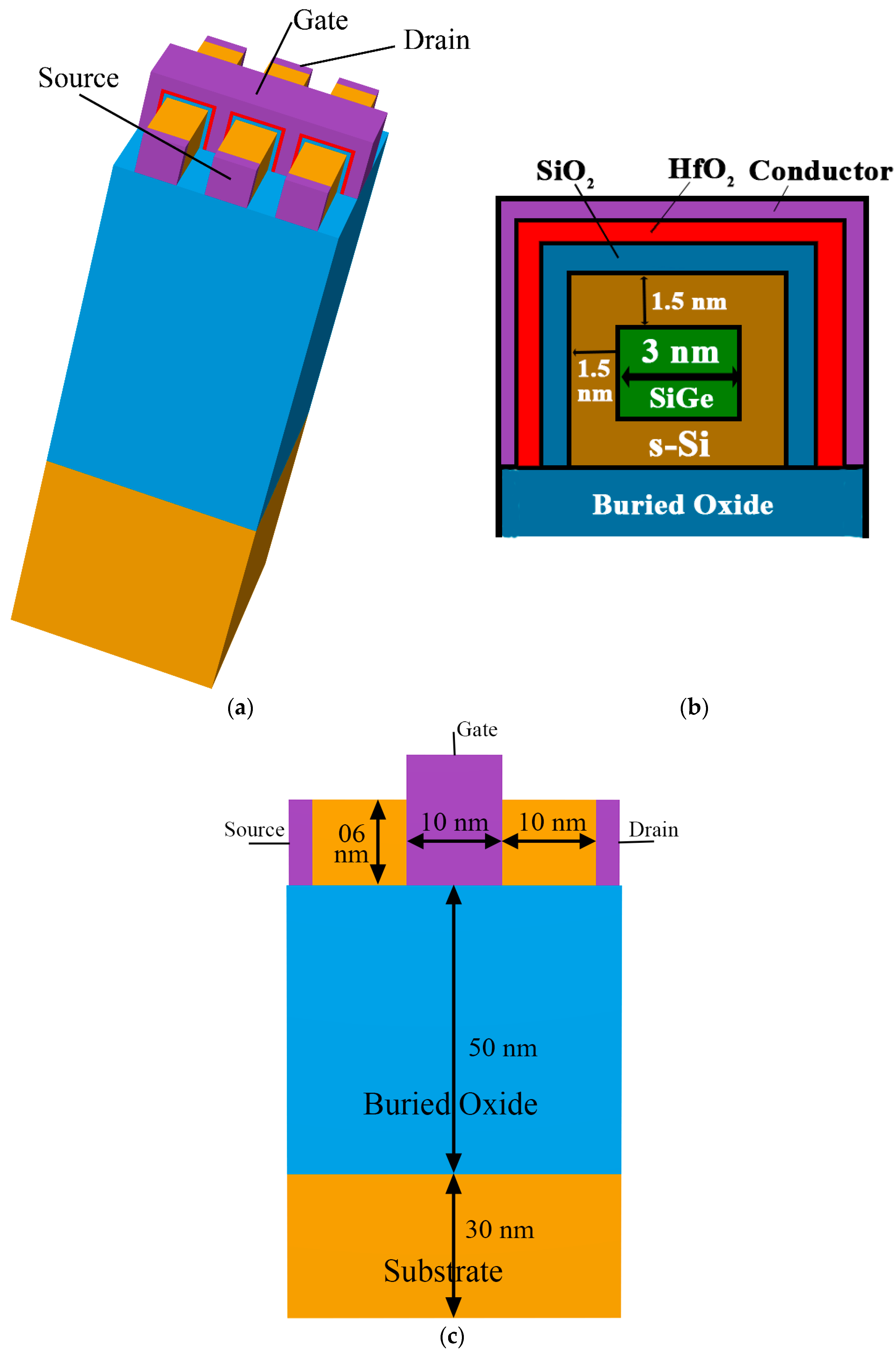
TG FinFETs containing different high-k dielectric materials are expected to be immensely beneficial for providing low off currents for the proposed device and, hence, an improvement in the device characteristics is expected. The device schematic was adjusted for a 10 nm channel length and is presented in
Figure 1. The physical width of the channel oxide was kept constant. Keeping the 1 nm physical thickness of the stacked high-k dielectric material fixed, the device modification was carried out for different high-k amounts in the device. Here, in this structure, to maintain the same physical thickness, 0.5 nm of high-k dielectric material over the channel region of the device was added on top of 0.5 nm of SiO
2, which was used as the stack gate oxide. The physical thickness of the high-k dielectric material layer used was 0.5 nm; hence, the total physical thickness was 1 nm, while the EOT was analyzed to determine the effective gate oxide thickness in the device. When using strained technology along with a high-k stack and a tri-layered silicon channel nanosystem in a three-fin FinFET, the control of the short-channel parameters is expected to be highly beneficial. The SiGe layer is placed in between two silicon layers, and a strained silicon region is developed, primarily forming a three-layered channel. As a result, the device is expected to provide enhanced performance due to induced strain in the channel for the 10 nm channel length FinFET, while improved off current is expected by controlling the SCEs through high-k gate oxide stack systems, which is the motivation of this paper.
The dimension specifics of the device are summarized in
Table 1, where the structure is presented placing three different layers on the channel. In the 10 nm three-fin HOI TG FinFET, the 1.5 nm thick silicon layer of the channel is strained and is displayed along with the 3 nm thick SiGe layer. Analysis of the device performance was carried out using Silvaco Atlas TCAD tools [
27]. The structure of the stacked high-k three-fin FinFET with a tri-layered strained silicon channel is displayed in
Figure 1. The physical dimensions and the EOT of all the high-k dielectrics used in the paper are tabulated in
Table 2.
3. Results and Discussion
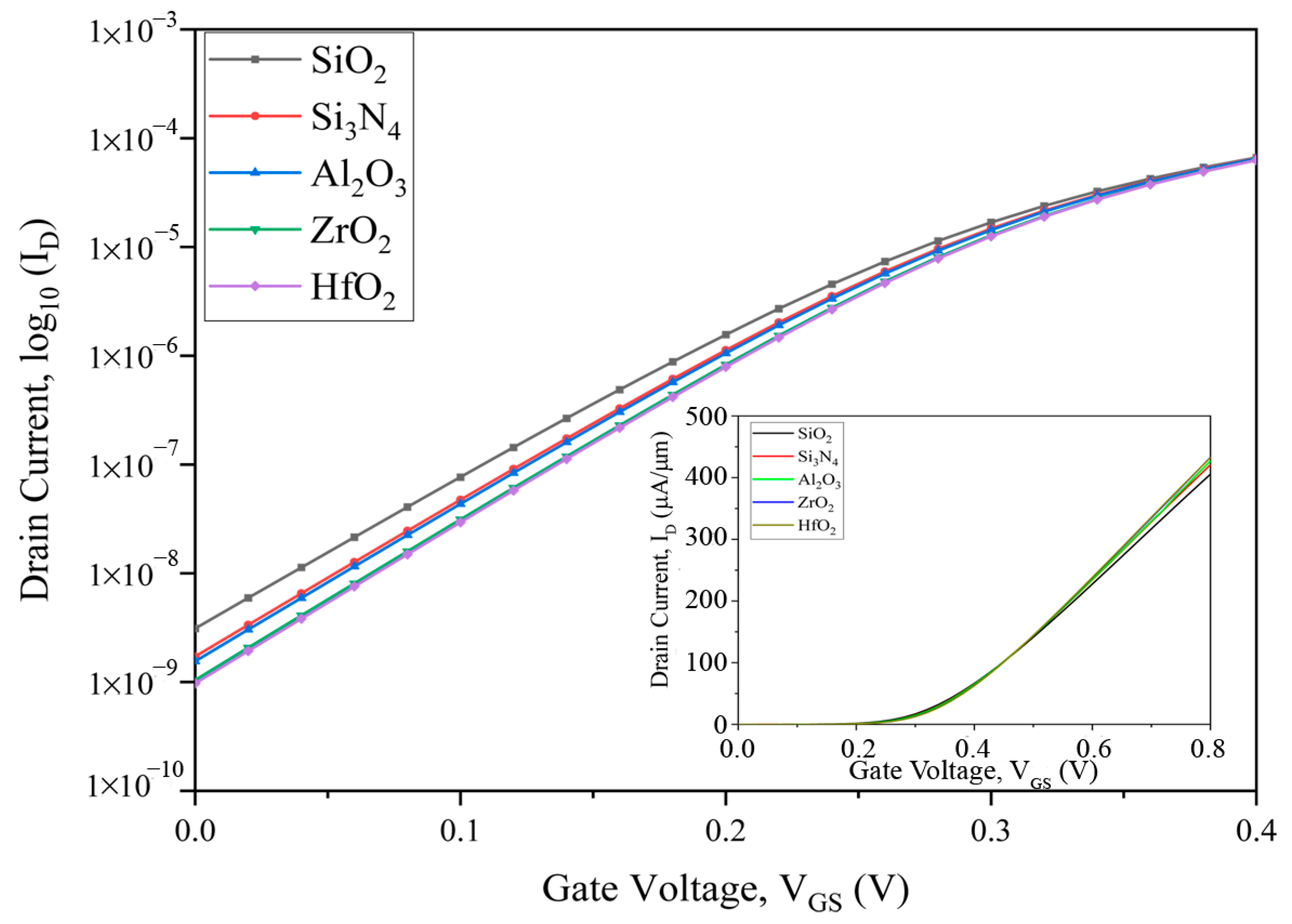
The linear (inside) and logarithmic characteristics graph of the stacked high-k three-fin strained TG FinFET is shown in
Figure 2. The drain current versus gate voltage transfer plots of the stacked high-k three-fin strained FinFETs with different stacked high-k gates are compared and plotted in
Figure 2, where the HfO
2-based devices show better performance. The logarithmic plot of drain current versus gate voltage displays the off current and SCE parameters for all the devices.
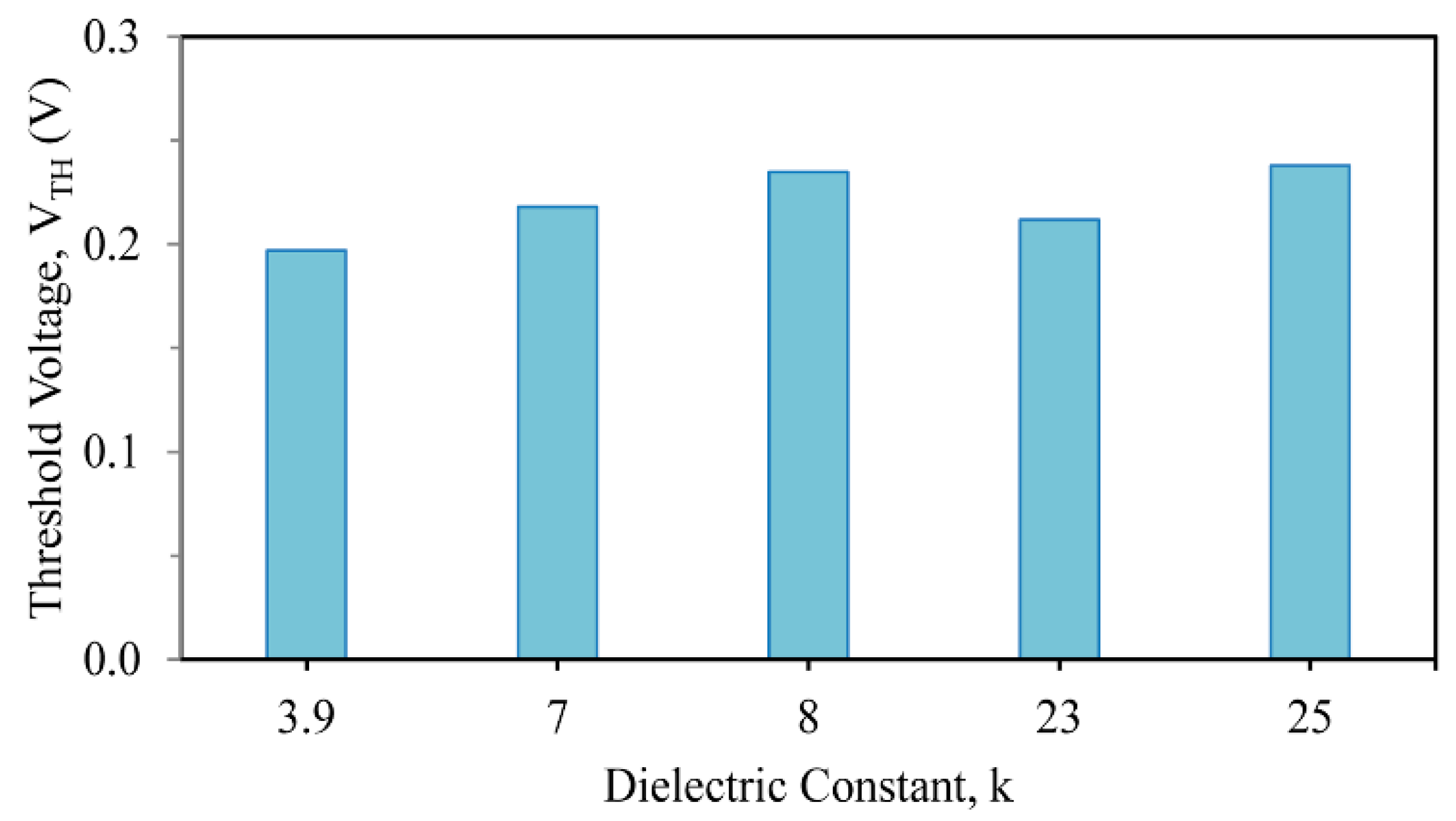
The threshold voltages (V
TH) of the developed devices with SiO
2 added to the high-k material (like Si
3N
4, Al
2O
3, ZrO
2, and HfO
2) to form the stack gate for the 10 nm three-fin TG FinFETs are calculated to be 0.218, 0.235, 0.212, and 0.238 V, respectively, as shown in
Figure 3. The device with only a SiO
2 gate has a threshold voltage of 0.197 V. A comparison of only the SiO
2 dielectric and stacked high-k dielectric materials was made, and it was observed that the HfO
2-based device had the highest threshold voltage; hence, a replacement for SiO
2 and other stacked high-k materials should be considered in the stacked arrangement for three-fin FinFET devices to provide improved voltage control.
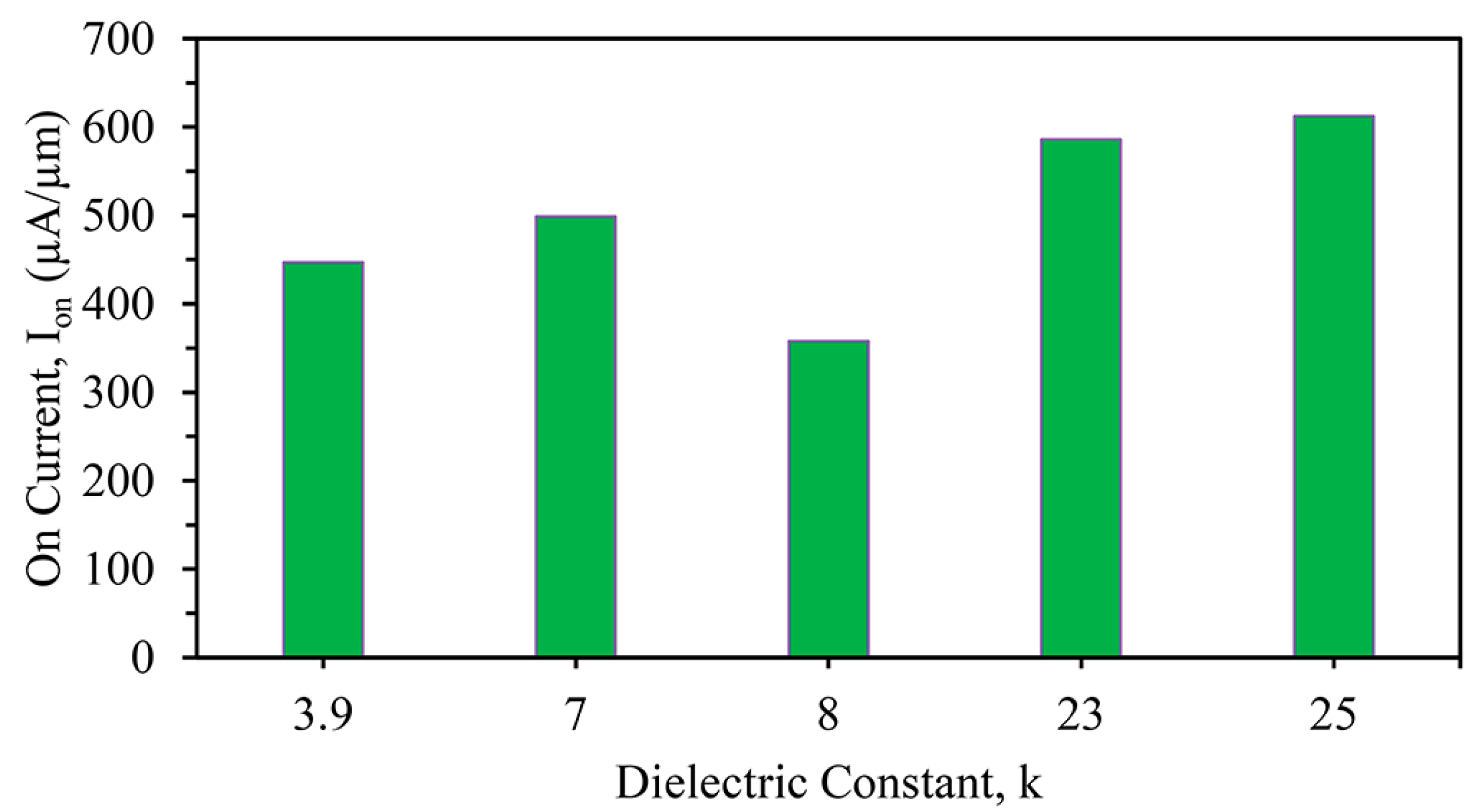
The on current (
Ion) was 446.54 μA/μm for the SiO
2-only device, whereas 498.90, 357.73, 585.92, and 612.24 μA/μm were observed, respectively, for the Si
3N
4-, Al
2O
3-, ZrO
2-, and HfO
2-based devices. The maximum on current was exhibited for the HfO
2 stacked high-k device due to the high dielectric value with an average work function, as seen in
Figure 4. This difference was due to the use of several gate metals in the three-fin device, in which the work functions were variable. The maximum on current (I
on) is clearly shown in
Figure 4.
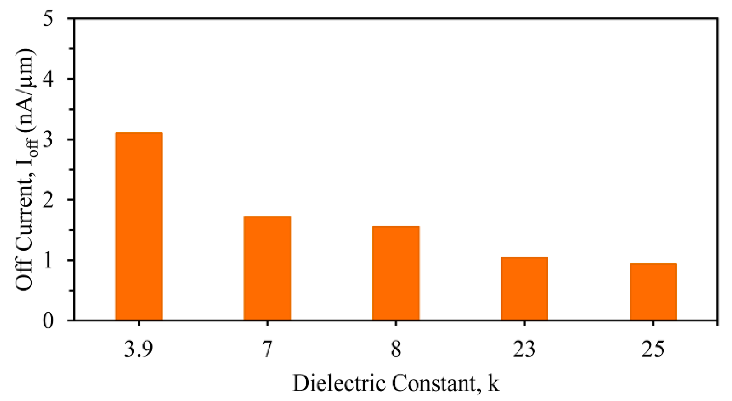
Thereafter, an analysis of the characteristics of the different material-based gate dielectric devices, like subthreshold swing, off current (
Ioff), and DIBL, was carried out to conclude which dielectric is suitable for the three-fin optimized device. The off current can be calculated using the below-mentioned formula [
28]:
where
W = the width of the channel and
L = the length of the channel,
VTH = the threshold voltage, and
SS = the subthreshold swing. The off current (
Ioff) variations for different gate dielectrics with high-k stacks were 0.94, 1.72, 3.11, 1.04, and 1.55 pA/μm for HfO
2, Si
3N
4, SiO
2, ZrO
2, and Al
2O
3, respectively, as displayed in
Figure 5. For improved device characteristics, the off current should be as low as possible, and it was found that the device with a SiO
2 and HfO
2 gate stacked oxide combination was the best alternative.
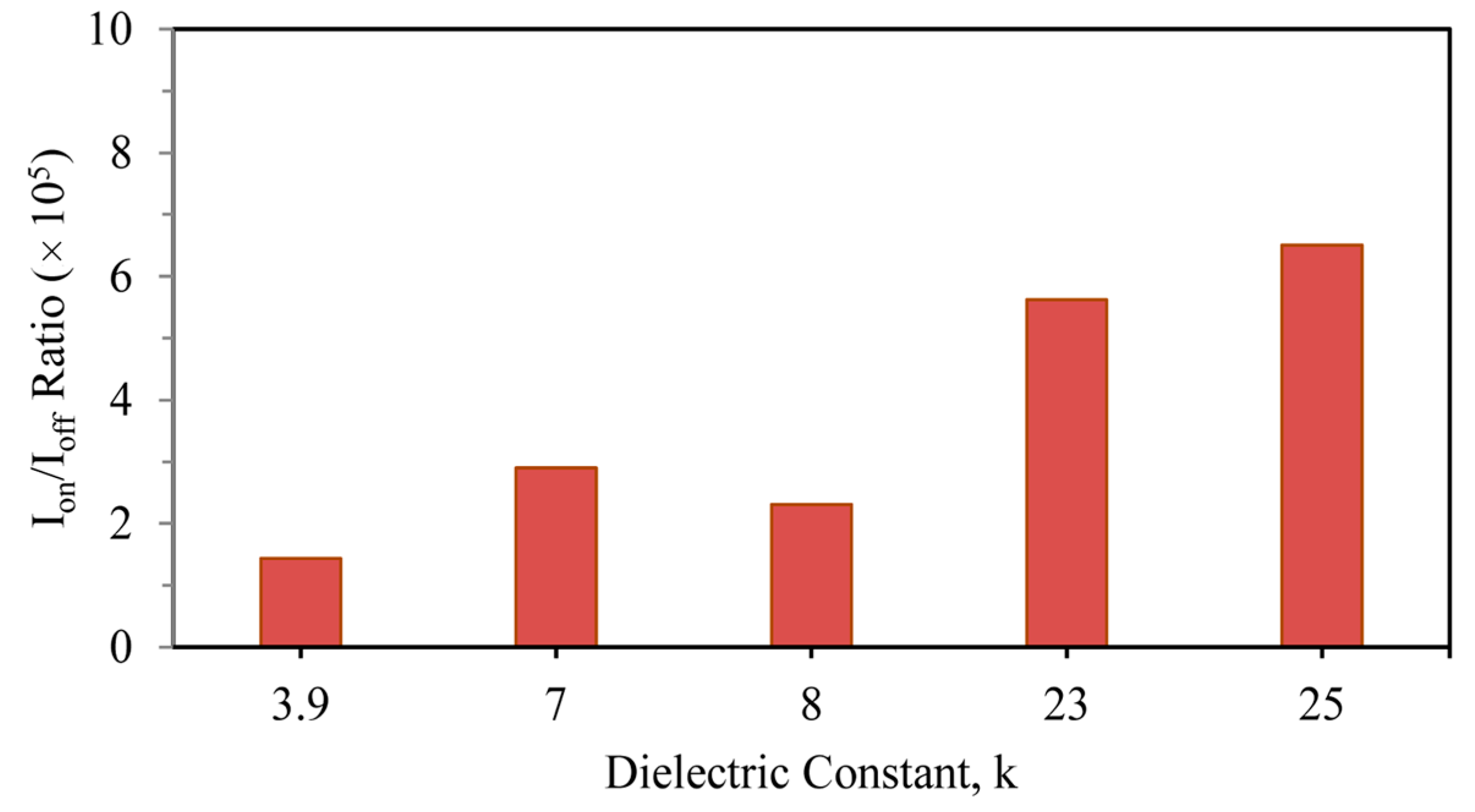
Next is the comparison of the
Ion/
Ioff ratio, which is shown in
Figure 6. For enhanced device performance, this ratio needs to be as high as possible. The
Ion/
Ioff factors for SiO
2, Si
3N
4, Al
2O
3, ZrO
2, and HfO
2 were observed to be 1.44, 2.90, 2.31, 5.62, and 6.51 (×10
5), respectively. So, the device structure with HfO
2 fulfils the requirement of providing the maximum on current with minimum leakage, so it can be concluded that the HfO
2 dielectric material as the gate oxide is the most suitable in a stacked three-fin strained-channel FinFET device.
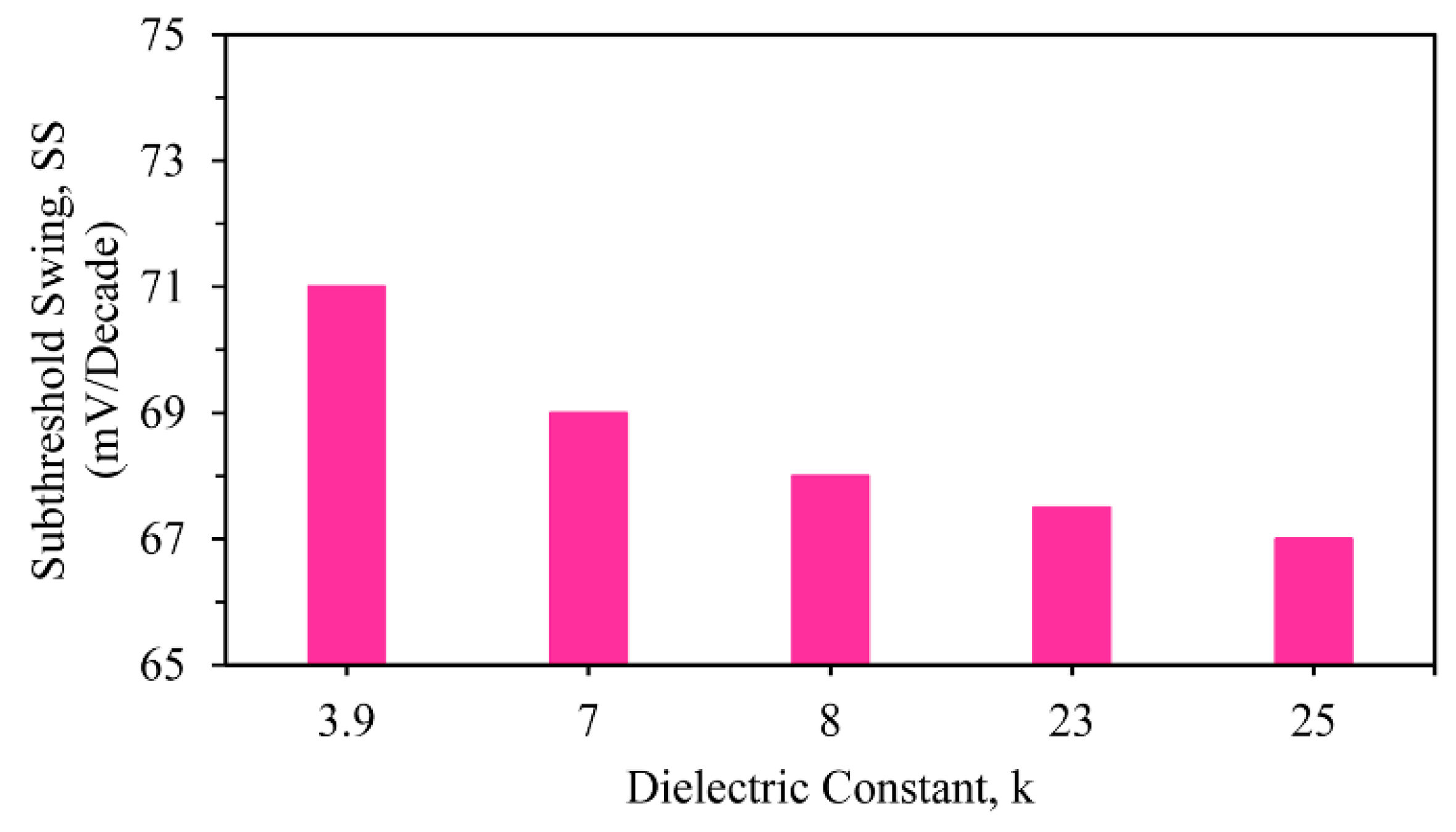
The next parameter, subthreshold swing, was analyzed using a linear plot, as shown in
Figure 7. Here, the value of subthreshold swing of the SiO
2 with HfO
2 was 67 mV/decade, whereas it was 71.05 mV/decade for the SiO
2-only device, thereby clearly showing that the stacked three-fin TG strained FinFET of SiO
2 + HfO
2 achieved enhanced performance in comparison to the others. For
SS calculation, we applied the following equation [
28]:
where
dVgs = the shift in the gate voltage and
d(
log10(
IDS)) = the shift in the logarithmic drain current. The variations in the
SS of different high-k stacked three-fin TG strained FinFETs are displayed in
Figure 7.
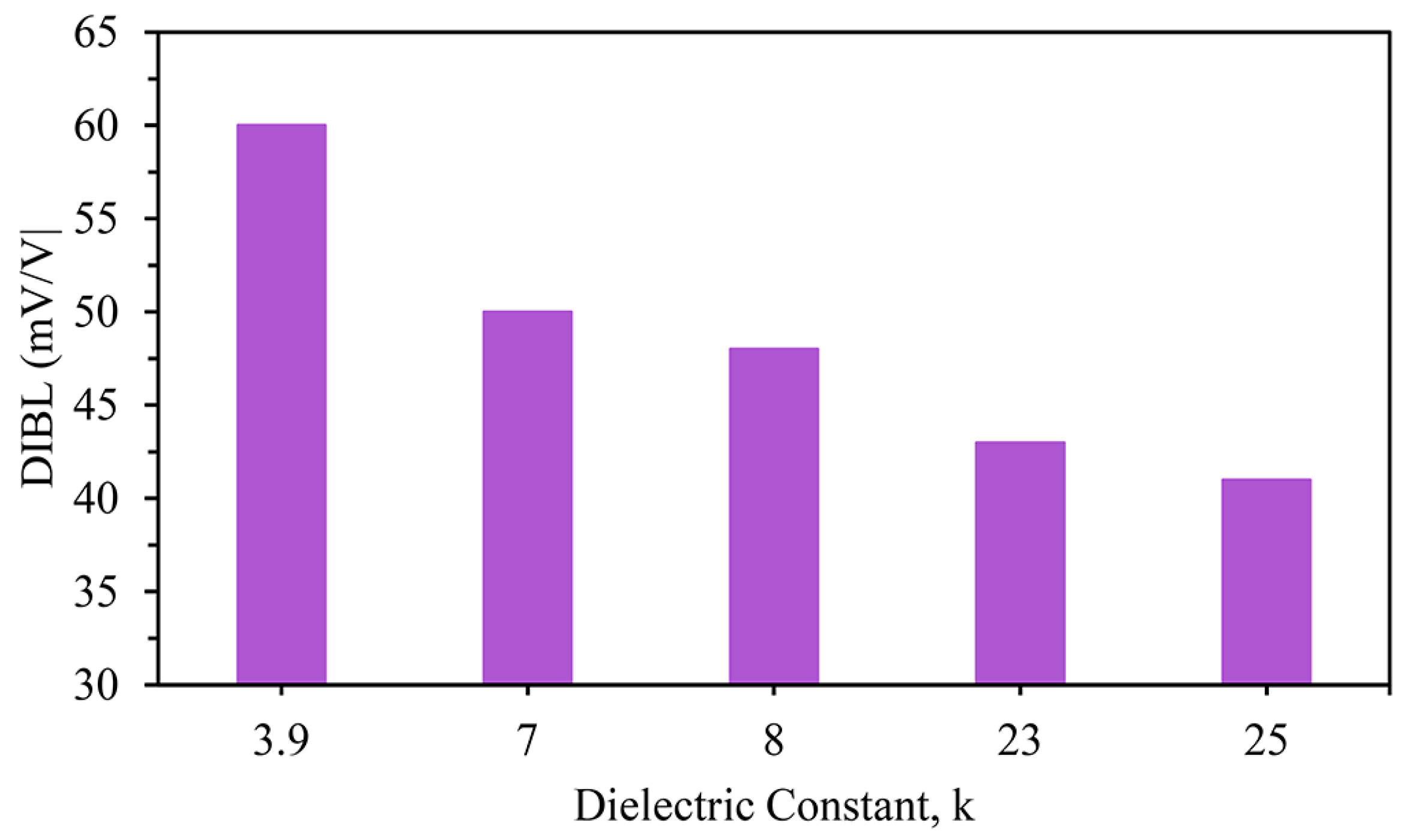
The last-compared factor presented here is the DIBL, and the results are shown in
Figure 8: 59.73, 49.78, 48.65, 42.90, and 40.99 mV/V for the SiO
2-only gate oxide material followed by the high-k stacks of Si
3N
4, Al
2O
3, ZrO
2, and HfO
2, respectively. The lowest DIBL value, and hence the best performance, was observed for the HfO
2-based device, as displayed in
Figure 8.
As a result, it is evident that the high-k dielectric material with a stacked arrangement of 0.5 nm of SiO2 and HfO2 of 0.5 nm physical thickness is the best fit to substitute SiO2 for managing SCEs at a channel length of 10 nm.
This demonstrates the effects of creating an enhanced three-fin technology device incorporating HfO2-based high-k material to improve the performance and meet the IRDS 2022 specifications for 3 nm technology node data.
Table 3 shows a detailed comparison, indicating better threshold voltage, on current, off current, SS, and DIBL for the 10 nm HOI high-k (HfO
2) stack than the existing 10 nm HOI three-fin FinFET; therefore, the former is considered to have enhanced performance in comparison to the standards suggested by IRDS 2022 [
21].
The 10 nm HOI high-k (HfO2) stack is reported to be adequate, despite the 82 mV/decade subthreshold swing (SS) as per IRDS 2022 for HP devices.
Quantum Results
In the gate, electrons are exhibited with regards to the semiconductor, and holes in the semiconductor are exhibited with regards to the gate.
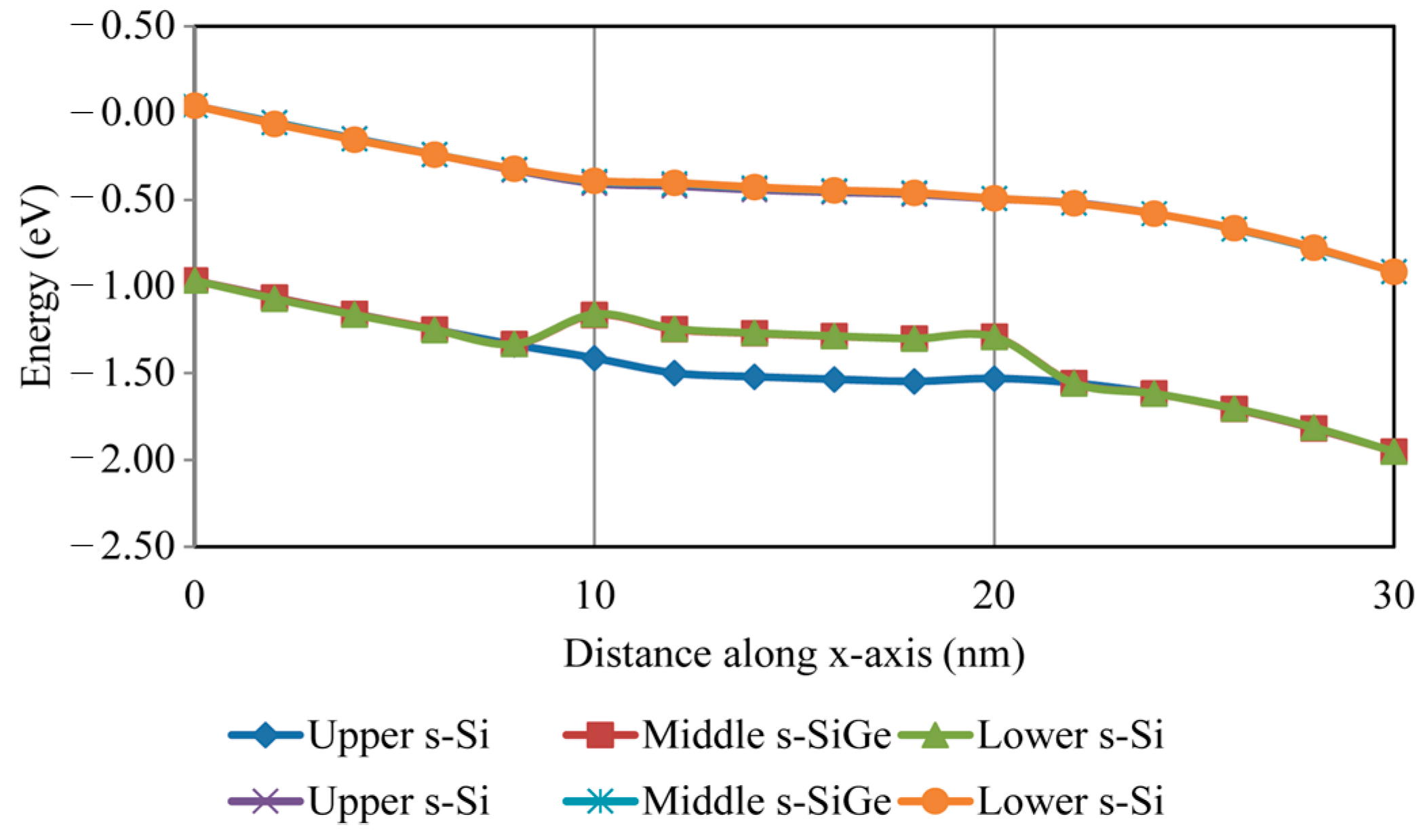
Figure 9 displays an energy band diagram of the accumulation region. In the semiconductor region, the band-bending curves were observed to rise. The middle s-SiGe and lower s-Si near the HOI structure are much closer to the conduction band than the valence band. From
Figure 9, it can be seen that the band cutline occurs in the strained-channel regions, where charge carriers are narrowed and confined towards the s-SiGe level, owing to the development of a quantum well arrangement in the channel. In the tri-layered channel, the effective mass due to the bandgap is reduced with the increased mobility of the carriers along with the biaxial strain incorporated into the channel region, which in turn affects the band bending in the quantum barrier of the channel in the nano-regime.
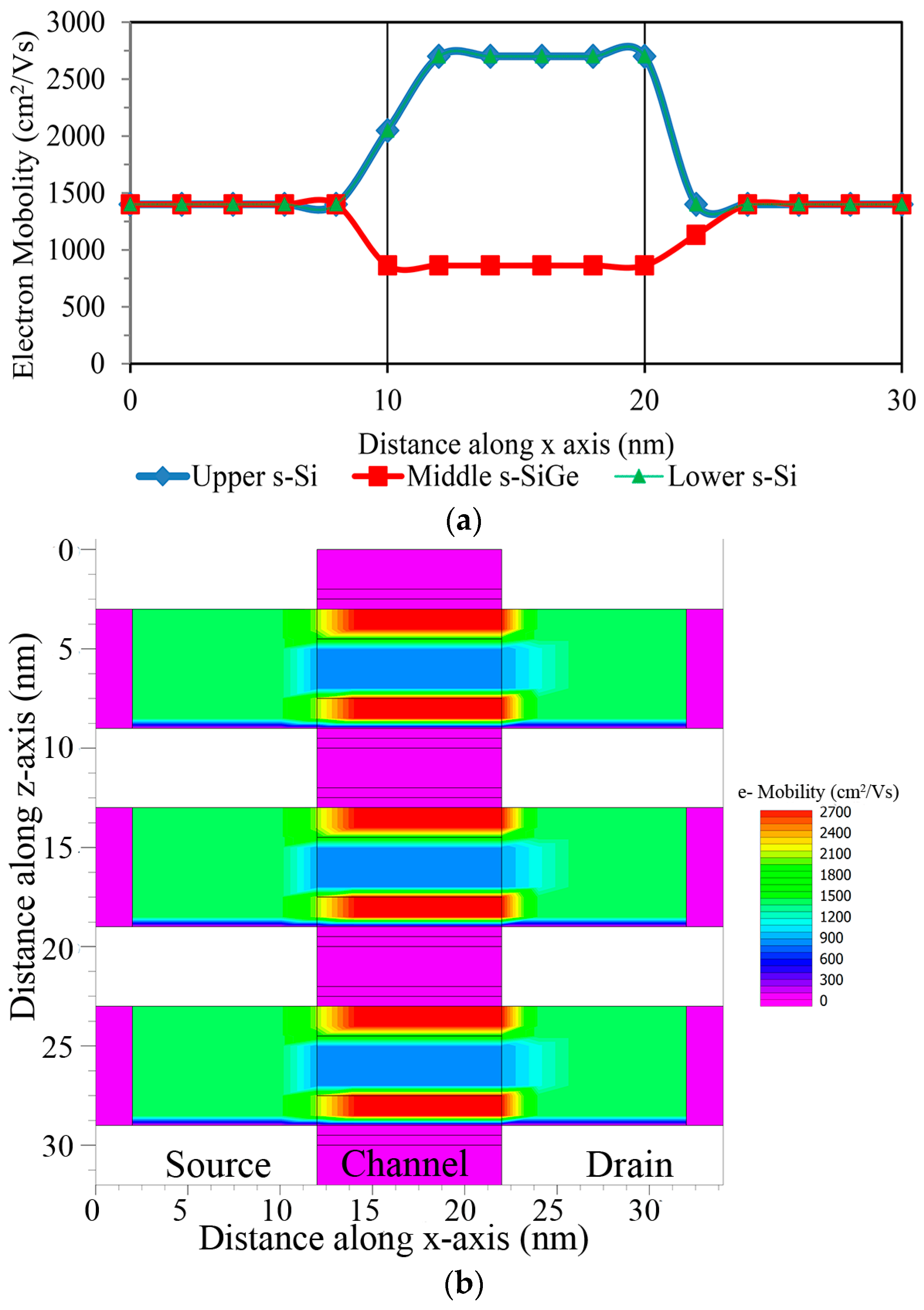
Owing to the reduced channel dimensions due to the effective mass, mobility is improved for the tri-layered strained silicon channel device. The currently developed device with an interfacial layer thickness of less than 2 nm and hafnium-based dielectrics has inferior electron mobility than the device with only a SiO
2 dielectric. The mobility exhibits more degradation via remote phonon scattering in the HfO
2 dielectric than the SiO
2 one, which can be successfully isolated by presenting a stacked high-k system in the tri-layered n-FinFET strained silicon technology device. Due to their quantization, the effective masses and charge carriers degenerate the strained silicon in the channel region, and, therefore, the mobility begins to increase. In the case of a tri-layered strained technology structure where high-k materials are used as the gate dielectric, the mobility is reduced to ~850 cm
2/Vs in the middle s-SiGe layer, whereas it increases to 2700 cm
2/Vs in the lower and upper s-Si layers, as clearly observed in
Figure 10a;
Figure 10b shows the mobility variation contour diagram. It was found that the HfO
2 dielectric was significantly more affected by remote phonon scattering than the SiO
2 dielectric, since the dielectric constant was high. From the electron mobility contour diagrams, increased electron mobility can be seen in the lower s-Si across the QW channel length, which is a strain-induced nano-regime structure with a 10 nm gate length for the 3 nm technology node, initiating quantum tunneling via ballistic transport using the s-SiGe well region. As a result of the shorter channel length (10 nm) of the device, ballistic transport occurs and only minor scattering roughness is observed in the system, which is undoubtedly witnessed in the mobility contours (
Figure 10b), indicating a smooth passage for electrons in the device across the strained-Si layer.
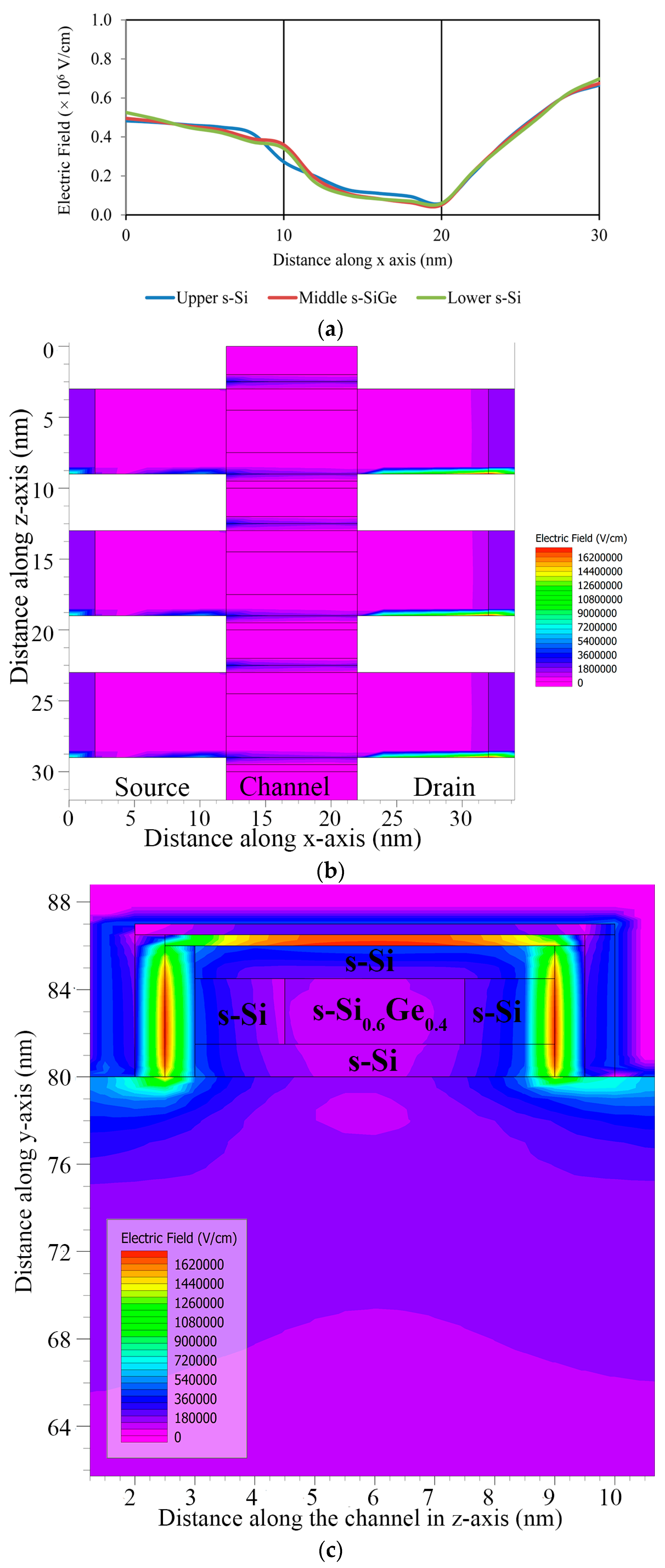
From the drain to source region, the electric field passes, allowing quantum carriers with minor constraint in the s-SiGe well region of the hetero-band structure channel in the quantum well barrier system to create a tunneling path, as shown in
Figure 11a. The contour for the electric field in the 10 nm gate length FinFET device is displayed in
Figure 11b,c. An extremely high electric field is noticeable due to the reduced gate length structure with an informal doped channel that introduces velocity saturation in the device. These interpretations are attributed to the occurrence of quasi-ballistic carrier transport because of the gate length limitation, which is induced by carrier regulation in the strain-induced thin s-Si well region of the quantum well barrier nanosystem device. This ballistic transport condition with carrier confinement is recognized in the HOI structure combination of the nano-channel device, which leads to the tunneling of the quantum charge carriers.
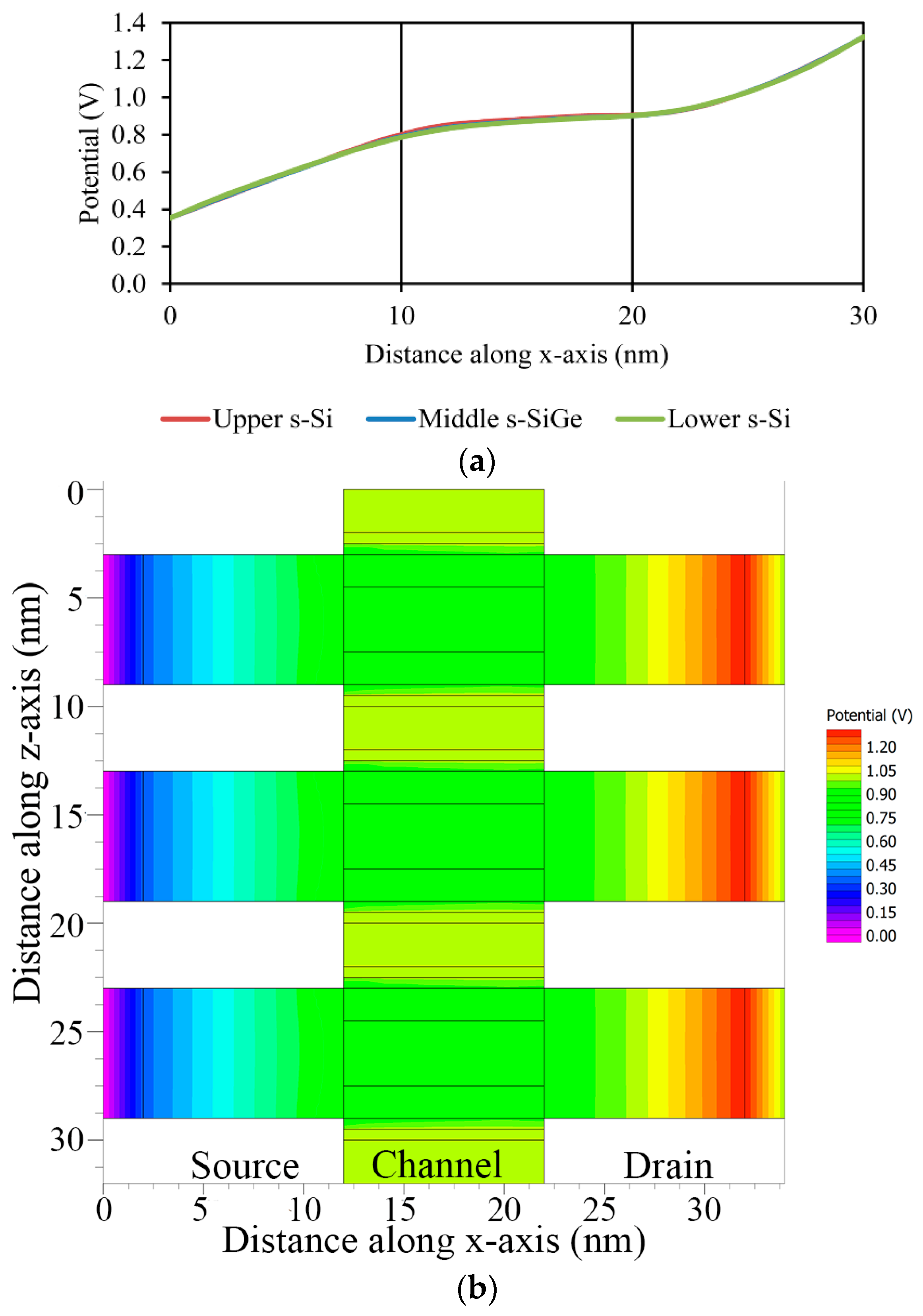
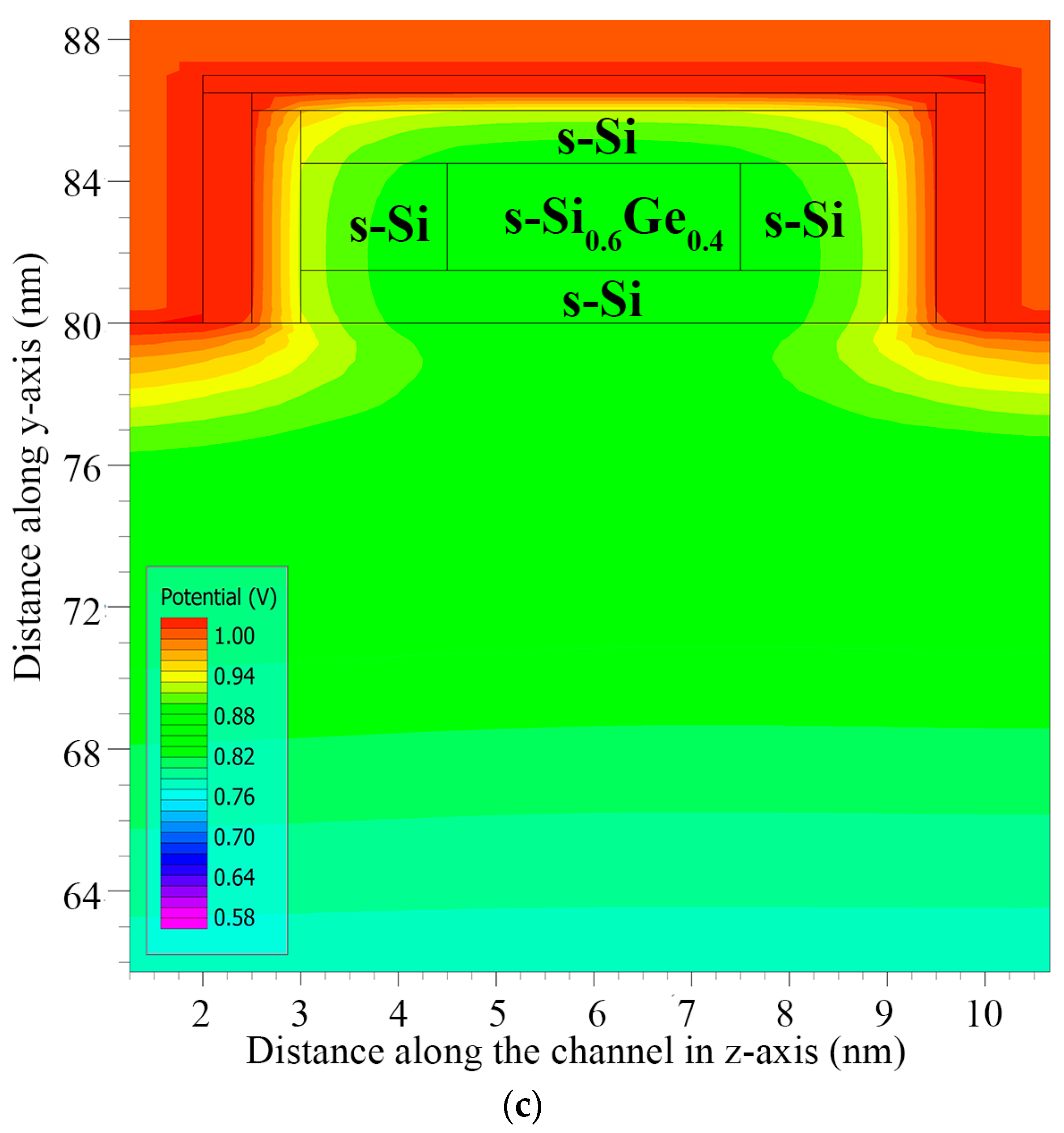
Concentrating on bandgap moderation, extreme electrostatic potential changes through s-SiGe deposition, concerning
Vgs for 1 V, were attained. The tri-gate FinFET with stacked high-k material established had a 10 nm channel length with 10
18 cm
−3 doping for the source and drain region; however, the tri-layered strained HOI quantum well barrier channel was moderately doped with a concentration of 10
15 cm
−3. The potential observed close to the source and the drain end increased with the increase in the drain voltage (
Vds), causing the potential of the inside strained layers to develop in the channel of the structure. The potential graph is shown in
Figure 12a, and a detailed analysis of the potential contours is displayed in
Figure 12b,c.
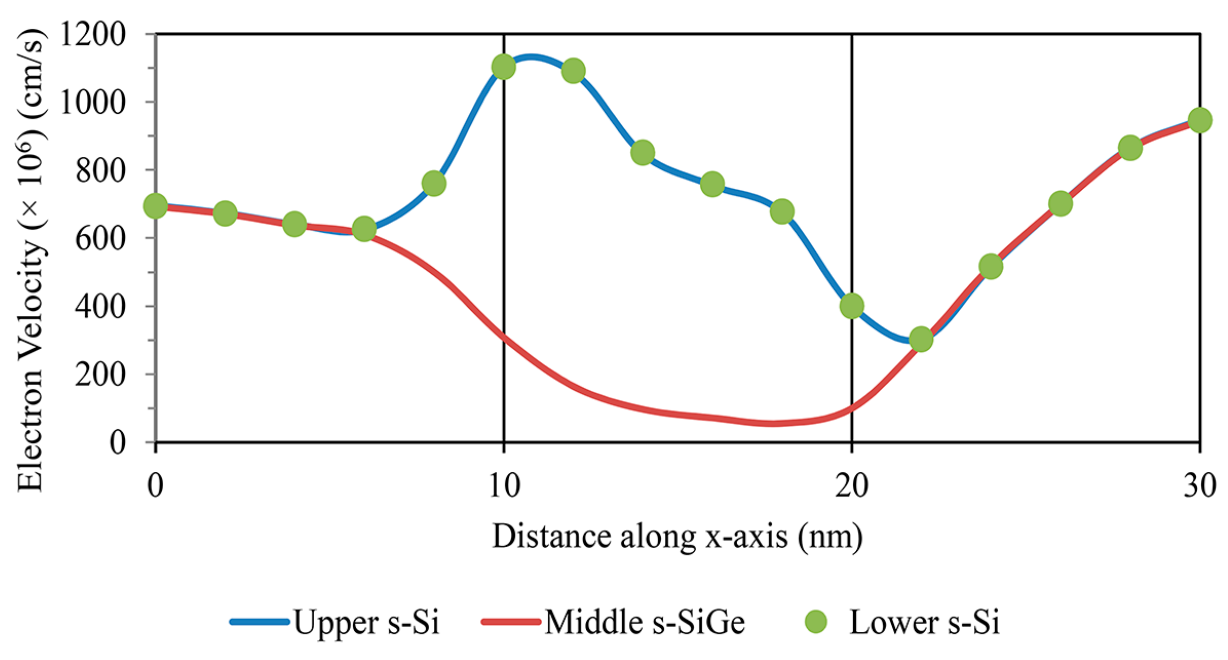
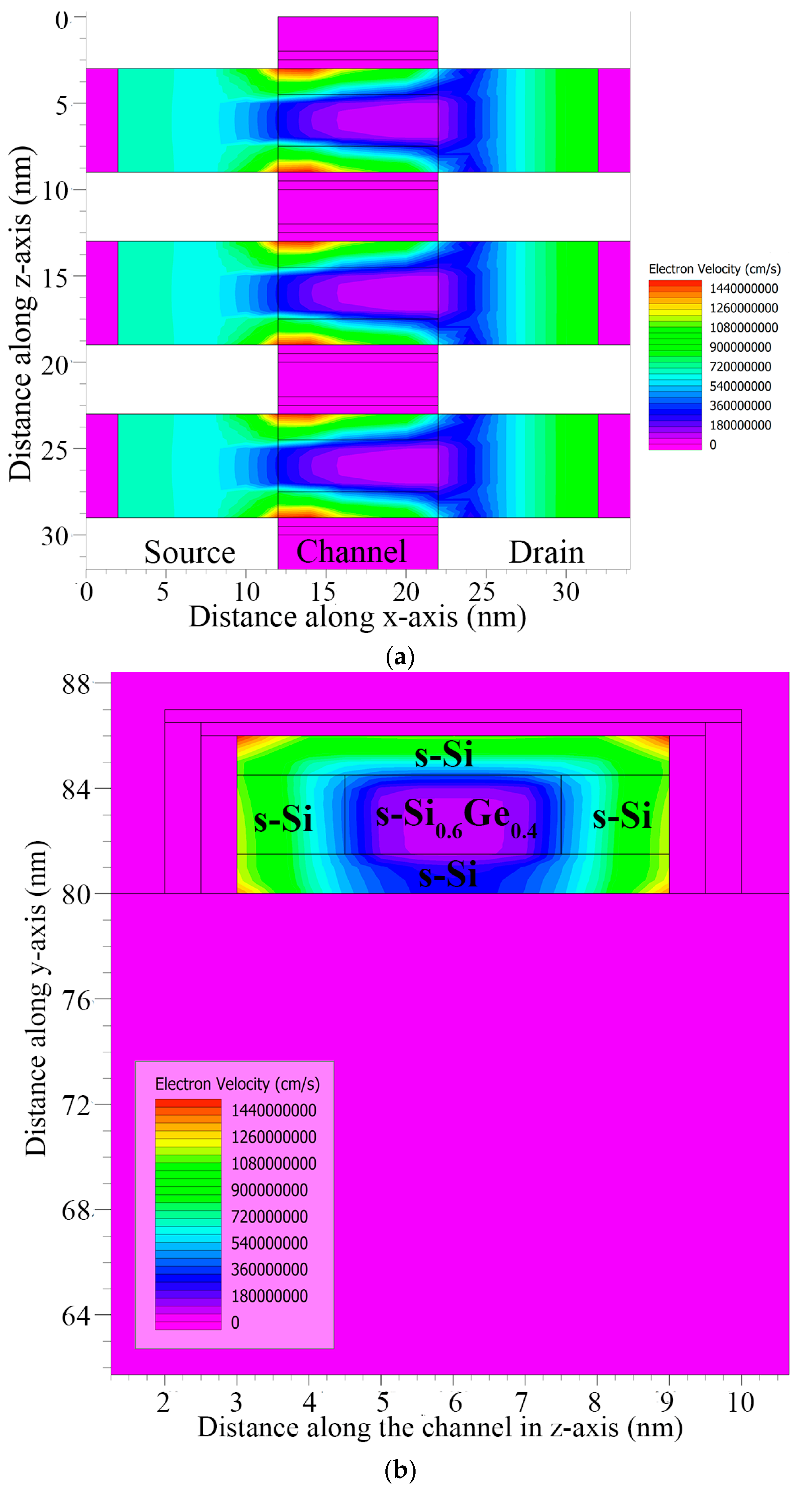
This improved mobility begins to act on the electron velocity, and the transformation of the TG strained-channel nano-FET device with a gate length of 10 nm is displayed in
Figure 13. The electron velocity was analyzed under extreme velocity conditions up to 1000 cm/s, as observed from the contour diagrams visualized in
Figure 14a,b for the shorter-gate-length device. This improvement in electron mobility gave increased drive current with extra electron velocity, while maintaining minimal gate-induced drain leakage in the device.
A high electron velocity and electric field in the strained-channel device were detected at the middle s-SiGe layer due to quantum carrier confinement. This is directly attributed to the improved carrier mobility with charge inversion occurring in the narrow- and reduced-channel-length devices with an s-SiGe well in the channel. It should be noted that due to the uniform electric field, the peak electron velocity was observed to be higher in the channel region.
In the strained-channel device, the mobility was improved because of the biaxial strain in the TG layered FinFET, while the SCEs induced an extreme inversion of the total charge density within the channel region; the doping variations at the fin edge and at the gate edge are displayed in
Figure 15.
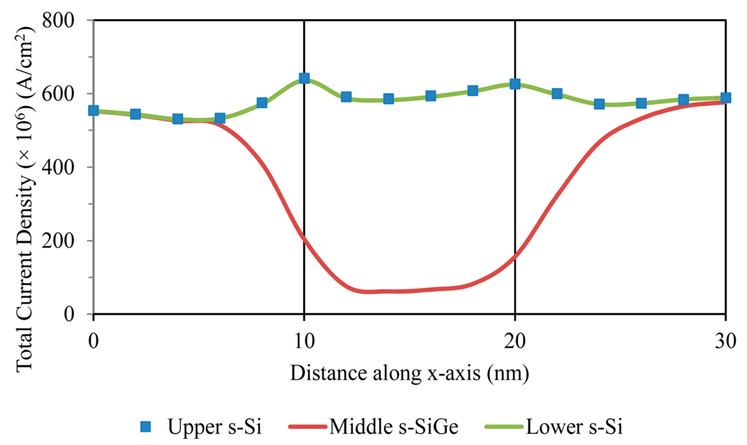
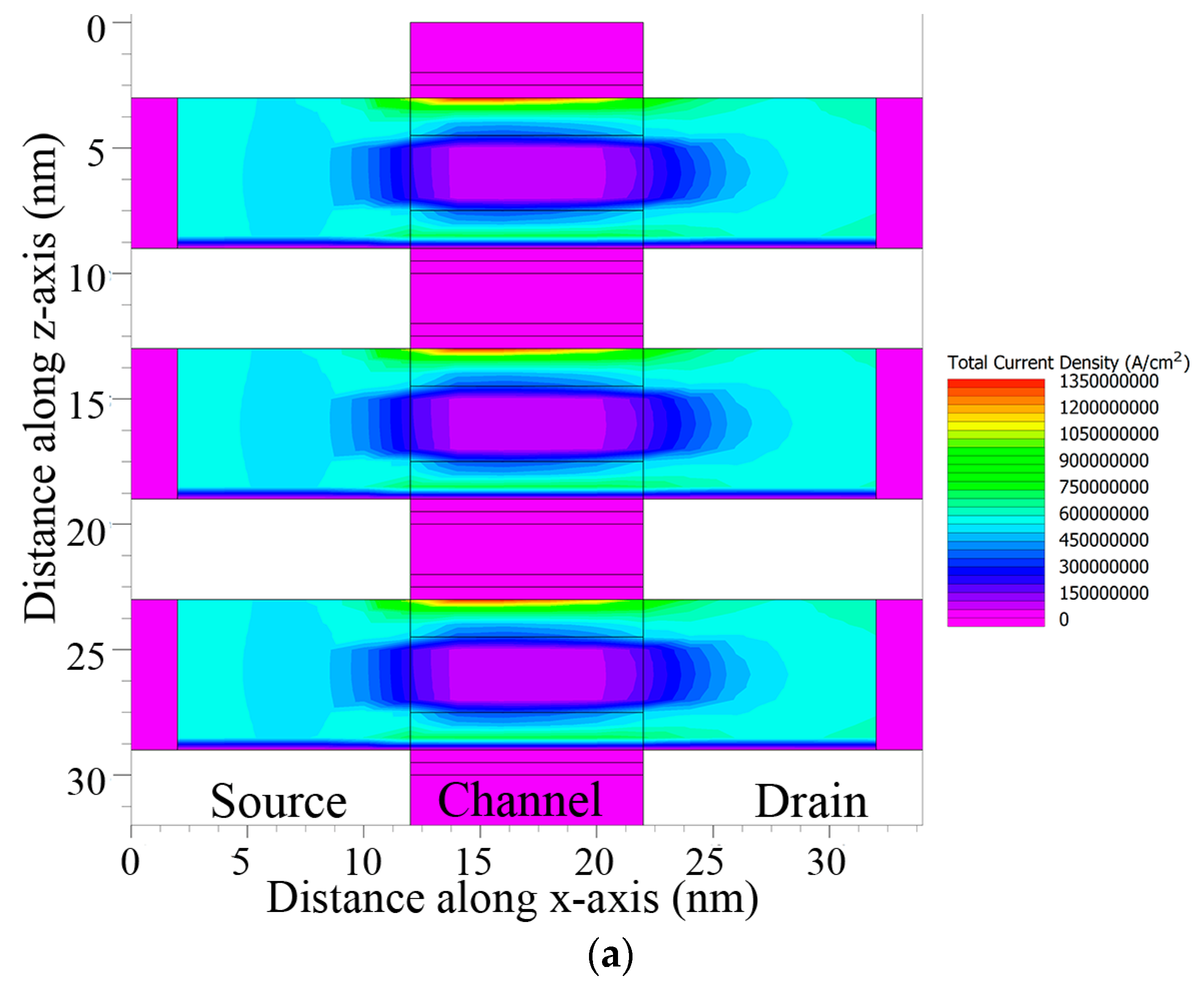
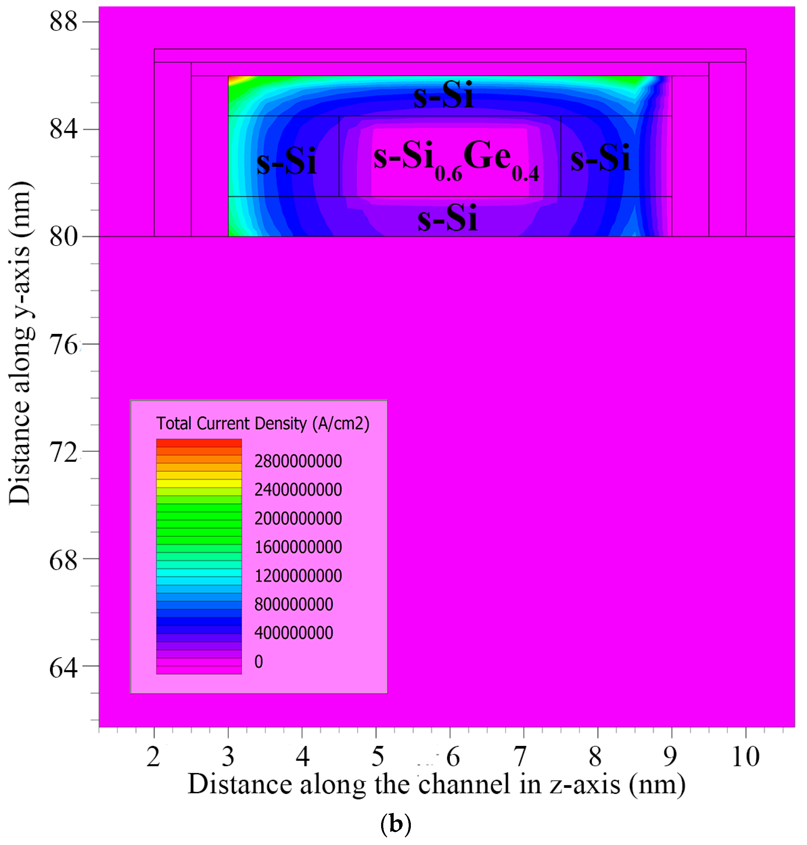
With the technically enriched gate control over the device, the current mostly passes through the upper s-Si region of the channel gate, while the middle s-SiGe layer experiences very low current, as depicted in
Figure 16a,b. Upon applying external bias via the electric field, the current flows through the strained silicon channel region. From the total current density graph, it can be observed that the current density was higher in the upper s-Si layer than the middle s-SiGe and lower s-Si layers, while the overall total current density was found to be 600 A/cm
2 from the contours in
Figure 16a,b.
4. Conclusions
Three-fin HOI n-FinFETs, using three-layered s-Si/SiGe/s-Si as 10 nm length channels, were developed here via the insertion of strain technology to extensively enhance the drive current of the devices. To this end, the gate oxides of the devices were built up in view of high-k stacks like Si3N4, ZrO2, Al2O3, and HfO2, keeping the physical thickness of the high-k material at 0.5 nm. The drain and source were fitted with a height and width of 6 nm. The threshold voltage, drive current, leakage current, Ion/Ioff current ratios, subthreshold swing, and DIBL were acquired for all the devices developed here and were compared. It was observed that the TG FinFETs’ performance was improved using strained silicon channels along with high-k stacked dielectrics, instead of a SiO2-only gate oxide. These three-fin strained stacked high-k devices provided reduced leakage current and enhanced drive current, particularly when adding HfO2-based high-k material. For the SiO2-only device, the VTH was 0.197 V, whereas for the stacked SiO2 and HfO2 device, the VTH was 0.238 V. Similarly, the DIBL for the stacked gate oxide device was 40.99 mV/V, which was quite low in comparison to the DIBL of 59.73 mV/V for the SiO2-only device. This proves that the device with HfO2 provided optimized results, performed the best, and had improved control over SCEs with very low leakage and improved switching. It was also observed through the cutline views of the band diagram that, due to its electron mobility, electric field, potential, electron velocity, and total current density, the HfO2-based stacked device is the most suitable alternative for the future.


