Abstract
The flat electronic band has remarkable relevance in the strongly correlated phenomena mainly due to its reduced kinetic energy in comparison to the many-body potential energy. The formation of such bands in cubically structured nanowires is addressed in this article by means of a new independent channel method and a generalized convolution theorem developed for the Green’s function including the first, second, and third neighbor interactions. A real-space renormalization method is further applied to address macroscopic-length aperiodic nanowires. We also determined the appearance condition of these flat bands, as well as their degeneracy and robustness in the face of perturbations, such as structural dislocations. Finally, the possible experimental detection of this flat band via the electronic specific heat is analyzed.
1. Introduction
In a crystalline solid, the null group velocity and infinite effective mass constitute the principal characteristics of a flat band, which is a highly degenerate energy level in the quantum mechanical point of view, in contrast to the massless Bloch electrons in two-dimensional hexagonal lattices. Heavy fermion metals represent a recognized example of flat bands formed by localized atomic orbitals [1]. Recently, topological flat bands originating from the geometrical interference of wave functions have significantly expanded the list of flat-band systems. The experimental realization of nearly flat bands has been achieved in Kagome materials, such as CoSn [2,3], Co3Sn2S2 [4], and YCr6Ge6 [5], as well as Moiré superlattices, such as twisted bilayer transition-metal dichalcogenides [6] and the twisted bilayer graphene [7], whose unconventional superconductivity observed at the magic angle has lately attracted significant attention [8]. In general, a large electronic density of states at the Fermi level induces a high superconducting transition temperature [9].
In recent decades, the research of materials at nanoscale has experienced exponential growth, revealing quantum phenomena in the macroscopic world. With a two-dimensional quantum confinement, the nanowires exhibit an exceptional itinerant ferromagnetism [10,11] and perform a crucial building-block role in nanoelectronics [12]. In this article, we report a real-space tight-binding study on the electronic band structure of nanowires built by cubically arranged atoms with interactions up to third neighbors. This study was carried out by means of a new independent channel method and a renewed convolution theorem, extending the previous one only for lattices with nearest neighbor interactions [13]. A real-space renormalization method [14] is further applied to address macroscopic-length aperiodic nanowires. The results show the formation of multiple flat electronic bands with a macroscopic number of degeneracies in each of them. These flat bands are robust under structural disorder perturbations, such as aperiodic dislocations, and can be observed by means of electronic specific heat measurements.
2. The Model
Let us consider a cubically structured nanowire with electron hopping between first, second, and third neighboring atoms, as shown in Figure 1 for a nanowire of atoms with and a transversal dislocation defect at the center of the figure characterized by first (), second (), and third () neighbor hopping integrals. The presence of such defects is common in nanowires since it very slightly alters the total free energy [15].
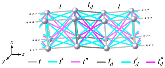
Figure 1.
Schematic representation of a nanowire with first (t), second , and third neighbor hopping integrals, as well as a dislocation characterized by , and .
The band structure of spinless electrons in this nanowire can be studied by means of a tight-binding Hamiltonian with null on-site energies given by
where considering possible transversal dislocations along the Z direction we have
and
which respectively describe the electron hopping between first, second, and third neighboring atoms. In Hamiltonians (2), (3), and (4), l, j, and k are integer numbers correspondingly counting atoms along the X, Y, and Z directions with wavefunctions in the Dirac notation as [16], where , , and are the one-dimensional Wannier functions [17].
Hamiltonian (1) with hopping integrals up to third neighbors can be rewritten as [18,19]
where symbol ⊗ denotes the Kronecker product, and with , for , and , being τ a dimensionless hopping integral with , , , and . Now we project Hamiltonian (5) on the eigenstates of the nanowire’s cross-section, which reduces it to an effective Z-directional Hamiltonian given by
where , , and [20]
Hamiltonian (6) can be rewritten as
where is the on-site energy and is the hopping integral of the ν-th Z-direction effective chain or channel with and . The condition for the existence of a fully disconnected channel with null hopping integrals or a highly degenerate flat band at energy equal to is
or
For example, a nanowire of atoms with an arbitrary integer number has a flat band at , if in (10), i.e., and . Alternatively, if and or in (10), the flat band will be located at . In the first case of , the degeneracy of the flat band is , while it is when , where is proportional to the length of nanowire. These degeneracy values were obtained from Equation (9). For instance, is a solution of Equation (10) when , and then there are four effective channels numbered by with all their hopping integrals equal to zero, which leads to a total degeneracy of .
On the other hand, the electronic density of states (DOS) can be calculated by means of the single-electron retarded Green’s function, determined by Hamiltonian (1) as [21]
where is the total number of atoms in the nanowire and
with , , , , and . Green’s function (12) can be rewritten as [13]
where
Since , i.e., is the eigenvalue of , Equation (13) becomes
Substituting (15) in (11), we obtain
or in the discrete form
where
Equations (8), (17), and (18) will be used in the numerical calculations of DOS by means of a real-space renormalization procedure applied to each effective channel ν, whose recursive formulas are given in Appendix A of Ref. [13].
3. Results
The electronic density of states (DOS) is plotted in Figure 2 as a function of the energy (E) with an imaginary part for periodic nanowires of atoms with (a, b) , , and , while (c, d) and , whose second and third neighbor hopping integrals are respectively and with (a) , (b) , (c) , and (d) .
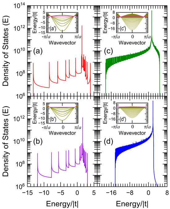
Figure 2.
Density of states (DOS) versus energy (E) for periodic nanowires of (a,b) 3 × 4 × 134,217,728 and (c,d) 35 × 35 × 165,580,142 atoms with , (a) , (b) , (c) , and (d) . The corresponding dispersion relations or band structures are shown in the insets (a′–d′), whose flat bands are plotted using magenta color lines.
The flat bands in Figure 2 are located at (a) , (b) , (c) , and (d) , whose degeneracies are (a) 4 × 134,217,728, (b) 3 × 134,217,728, and (c,d) 35 × 16,558,042. These degrees of degeneracy were obtained from Equation (9). The rest of the peaks in Figure 2a–d are the van Hove singularities originating from each independent channel. The dispersion relations E(k), where k is the wavevector along the Z direction, are shown in the insets (a′–d′) using unit cells of (a′,b′) 3 × 4 and (c′,d′) 35 × 35 atoms, where the flat bands are plotted as magenta color lines.
The total electronic energy () for a given band filling (ρ) can be calculated as [22]
where is the Fermi–Dirac distribution with the Boltzmann constant and temperature T, whose chemical potential µ is determined by
In other words, for a given ρ and T, the chemical potential μ is firstly evaluated from (20) and then the total electronic energy is calculated using (19). The constant-volume electronic specific heat () per electron is given by
where
is the number of electrons in the nanowire for each band filling ρ that produces a specific chemical potential μ in the Fermi–Dirac distribution .
In Figure 3a,b, the electronic specific heat () as a function of the band filling (ρ) and temperature (T) is shown respectively for the nanowires of Figure 2a,b. Notice the maximums around come from the flat bands in DOS, whose presence can be analyzed using the Sommerfeld expansion for low temperatures given by [22]
i.e., the electronic specific heat linearly grows with T, whose slope is proportional to and could be extremely large when μ is located at the flat band, as occurred at the maximums in Figure 3a,b. The difference of these two maximums in height and width is derived from that the flat band in Figure 3a contains a third part of the total electronic states, while in Figure 3b the flat band has only a fourth part. For example, the peak of in Figure 3a begins at band filling ρ ≃ 42.3% and ends at ρ ≃ 74.6%, while in Figure 3b it begins at ρ ≃ 60.5% and ends at ρ ≃ 84.7%. The ratio of these two peak widths is approximately .
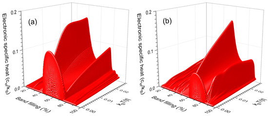
Figure 3.
Electronic specific heat () versus the band filling (ρ) and temperature (T) for periodic nanowires of 3 × 4 × 134,217,728 atoms with (a) and (b) .
To illustrate more effects of the flat band, variations in the chemical potential (μ), electronic energy (), and specific heat () as functions of the temperature (T) are plotted in Figure 4 for the same nanowire of Figure 3a with band fillings of (a–c) 40%, (a′–c′) 58%, and (a″–c″) 77%, respectively corresponding just below, at, and over the flat-band fillings.
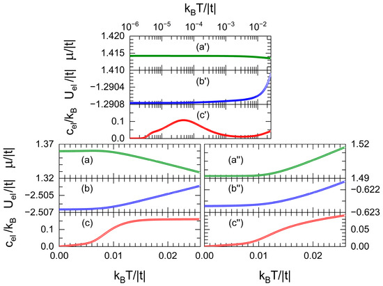
Figure 4.
Chemical potential (μ), electronic energy () and specific heat () versus the temperature (T) for the same nanowire of Figure 3a with band fillings of (a–c) 40%, (a′–c′) 58%, and (a″–c″) 77%.
In Figure 4b,b′,b″, the permanent growth of electronic energy with temperature (T) can be observed, since more electrons are excited into higher energy states for larger T, in contrast to the decreasing, almost constant, and increasing behaviors of the chemical potential (μ) respectively shown in Figure 4a,a′,a″. For example, the diminution of μ in Figure 4a is needed to keep a constant band filling of 40%, because such μ is located below the energy of flat-band states, and, at high temperature, a fraction of the total probability is shifted to larger energy states with a huge DOS, as stated by the Fermi–Dirac distribution. In a similar way, for μ larger than the flat-band energy, this shift of probability to higher energies with small DOS causes a growth of μ to preserve a constant band filling at large T.
Note in Figure 4c the peak of electronic specific heat () in logarithm scale draw when μ is located at the flat band. The rapid growth of this peak was discussed previously via Equation (23), while its quick decrease is related to the vanishing of occupation probability around μ at high temperatures predicted by the Fermi–Dirac distribution. In fact, the ubication of this peak close to is associated with the imaginary part used in these calculations.
Now, let us introduce transversal dislocations with hopping integrals into the nanowires, as shown in Figure 1. These dislocations are inserted following the Fibonacci quasiperiodic sequence , i.e., with the initial conditions of and [14], where ⊕ denotes the concatenation of two previous generations, A and B respectively represent hopping integrals t and . In addition, we will keep the first m generations of the Fibonacci sequence without dislocations and introduce the first in the generation , placing it at the union of generations and . For example, if , we have , , , , etc.
In Figure 5, the electronic density of states (DOS) is plotted as a function the single-electron energy (E) with an imaginary part of for nanowires of 35 × 35 × 165,580,142 atoms containing 10,947 (violet line), 121,394 (pink line), 1,346,270 (orange line), and 14,930,353 (dark-yellow line) dislocations that respectively correspond to . The second- and third-neighbor hopping integrals of these nanowires are respectively and , while their dislocations are characterized by hopping integrals (a) , , and , as well as (b) , , and . The length of such nanowires corresponds to a Fibonacci sequence of generation .
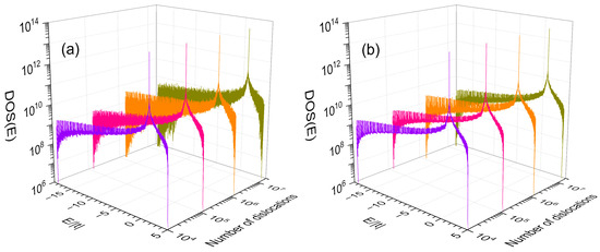
Figure 5.
Electronic density of states (DOS) versus energy (E) with for nanowires of 35 × 35 × 165,580,142 atoms, 10,947 (violet line), 121,394 (pink line), 1,346,270 (orange line), and 14,930,353 (dark-yellow line) dislocations with , : (a) and (b) .
The high frequency oscillations of DOS along whole spectrum can be observed, whose amplitude grows with the number of dislocations, except the flat-band states remain intact. These oscillations originate from the presence of dislocations and are more notable when the difference grows.
4. Conclusions
This article presented a new independent channel method for cubically structured nanowires with first, second, and third neighbor hopping interactions, as well as a generalized convolution theorem for the single-electron Green’s function of such nanowires. The former analytically demonstrates the possible existence of flat bands and provides their appearance conditions, as well as their degrees of degeneracy, while the latter permits an efficient calculation of the density of states (DOS), as well as other physical quantities based on the Green’s function, such as the electrical conductivity via the Kubo–Greenwood formula [13].
As an example, a detailed study of a narrow nanowire of atoms, where is a macroscopic integer number, was reported, whose DOS spectrum confirms the existence of a flat band with a macroscopic degree of degeneracy, and the presence of such a flat band may significantly alter the spectrum of electronic specific heat (). This new spectrum of derived from the flat band can be experimentally measured, if we were able to synthesize nanowires that nearly satisfy the analytical relationship found in this article between the first, second, and third hopping-integral strengths by applying an external pressure, while the variation in band filling could be achieved via the application of a gate voltage. The assumption of and can be closely satisfied, if the hopping integral scales almost exponentially with the interatomic distance (d) such as , which leads to and for s orbitals, where a is the nearest-neighbor interatomic distance and is a reference length. Hence, a hydrostatic external pressure may simultaneously modify the ratios and to eventually satisfy the flat-band appearance condition such as in the analyzed cases.
Finally, the results of this article also reveal the robustness of such a flat band in spite of the geometrical interference of wave functions induced by structural perturbations, such as the transversal dislocations that frequently appear in nanowires since they very slightly alter the total free energy. It would be worth mentioning that the independent channel method and convolution theorem reported in this article combined with the renormalization method [14] permit the development of a real-space quantum theory of solids and devices containing defects and structural interfaces, such as PNP and NPN transistors, as well as segmented nanowires for thermoelectric applications [23]. This development is currently in progress.
Author Contributions
Conceptualization, V.S. and C.W.; methodology, V.S. and C.W.; software, V.S. and C.W.; validation, V.S. and C.W.; formal analysis, V.S. and C.W.; investigation, V.S. and C.W.; resources, V.S. and C.W.; writing—original draft preparation, V.S. and C.W.; writing—review and editing, V.S. and C.W.; funding acquisition, V.S. and C.W. All authors have read and agreed to the published version of the manuscript.
Funding
This research has been partially supported by the Consejo Nacional de Humanidades, Ciencias y Tecnologías via grant CF-2023-I-830 and by the National Autonomous University of Mexico (UNAM) through projects PAPIIT-IN112522 and PAPIIT-IN110823. The computations were performed at Miztli of DGTIC-UNAM.
Data Availability Statement
Data sharing not applicable.
Acknowledgments
The technical assistance of Alejandro Pompa, Oscar Luna, and Silvia E. Frausto is fully appreciated.
Conflicts of Interest
The authors declare no conflict of interest.
References
- Shaginyan, V.R.; Alfred, Z.; Msezane, A.Z.; George, S.; Japaridze, G.S. Peculiar physics of heavy-fermion metals: Theory versus experiment. Atoms 2022, 10, 67. [Google Scholar] [CrossRef]
- Kang, M.; Fang, S.; Ye, L.; Po, H.C.; Denlinger, J.; Jozwiak, C.; Bostwick, A.; Rotenberg, E.; Kaxiras, E.; Checkelsky, J.G.; et al. Topological flat bands in frustrated Kagome lattice CoSn. Nat. Commun. 2020, 11, 4004. [Google Scholar] [PubMed]
- Liu, Z.; Li, M.; Wang, Q.; Wang, G.; Wen, C.; Jiang, K.; Lu, X.; Yan, S.; Huang, Y.; Shen, D.; et al. Orbital-selective Dirac fermions and extremely flat bands in frustrated Kagome-lattice metal CoSn. Nat. Commun. 2020, 11, 4002. [Google Scholar] [PubMed]
- Yin, J.-X.; Zhang, S.S.; Chang, G.; Qi Wang, Q.; Tsirkin, S.S.; Guguchia, Z.; Lian, B.; Zhou, H.; Jiang, K.; Belopolski, I.; et al. Negative flat band magnetism in a spin-orbit-coupled correlated Kagome magnet. Nat. Phys. 2019, 15, 443–448. [Google Scholar]
- Wang, P.; Wang, Y.; Zhang, B.; Li, Y.; Wang, S.; Wu, Y.; Zhu, H.; Liu, Y.; Zhang, G.; Liu, D.; et al. Experimental observation of electronic structures of Kagome metal YCr6Ge6. Chin. Phys. Lett. 2020, 37, 087102. [Google Scholar] [CrossRef]
- Zhang, Z.; Wang, Y.; Watanabe, K.; Taniguchi, T.; Ueno, K.; Tutuc, E.; LeRoy, B.J. Flat bands in twisted bilayer transition metal dichalcogenides. Nat. Phys. 2020, 16, 1093–1096. [Google Scholar] [CrossRef]
- Kim, K.; DaSilva, A.; Huang, S.; Fallahazad, B.; Larentis, S.; Taniguchi, T.; Watanabe, K.; LeRoy, B.J.; MacDonald, A.H.; Tutuc, E. Tunable Moiré bands and strong correlations in small-twist-angle bilayer graphene. Proc. Natl. Acad. Sci. USA 2017, 114, 3364–3369. [Google Scholar] [CrossRef] [PubMed]
- Cao, Y.; Fatemi, V.; Fang, S.; Watanabe, K.; Taniguchi, T.; Kaxiras, E.; Jarillo-Herrero, P. Unconventional superconductivity in magic-angle graphene superlattices. Nature 2018, 556, 43–50. [Google Scholar] [CrossRef] [PubMed]
- Balents, L.; Dean, C.R.; Efetov, D.K.; Young, A.F. Superconductivity and strong correlations in Moiré flat bands. Nat. Phys. 2020, 16, 725–733. [Google Scholar] [CrossRef]
- Vaitiekėnas, S.; Liu, Y.; Krogstrup, P.; Marcus, C.M. Zero-bias peaks at zero magnetic field in ferromagnetic hybrid nanowires. Nat. Phys. 2021, 17, 43–47. [Google Scholar] [CrossRef]
- Ziti, I.; Britel, M.R.; Bouajaj, A.; Wang, C. Quantum confinement and surface effects on the itinerant ferromagnetism in Ni and Ni–Fe nanowire arrays: An ab initio study. Phys. Status Solidi B 2018, 255, 1700618. [Google Scholar] [CrossRef]
- Jia, C.; Lin, Z.; Huang, Y.; Duan, X. Nanowire electronics: From nanoscale to macroscale. Chem. Rev. 2019, 119, 9074–9135. [Google Scholar] [CrossRef] [PubMed]
- Sánchez, V.; Wang, C. Application of renormalization and convolution methods to the Kubo-Greenwood formula in multidimensional Fibonacci systems. Phys. Rev. B 2004, 70, 144207. [Google Scholar] [CrossRef]
- Sánchez, V.; Wang, C. Real space theory for electron and phonon transport in aperiodic lattices via renormalization. Symmetry 2020, 12, 430. [Google Scholar] [CrossRef]
- Mikkelsen, A.; Sköld, N.; Quattara, L.; Borgström, M.; Andersen, J.N.; Samuelson, L.; Seifert, W.; Lundgren, E. Direct imaging of atomic structure inside a nanowire by scanning tunneling microscopy. Nat. Mater. 2004, 3, 519–523. [Google Scholar] [CrossRef] [PubMed]
- Bruus, H.; Flensberg, K. Many-Body Quantum Theory in Condensed Matter Physics, an Introduction; Oxford University Press: Oxford, UK, 2016; pp. 3–9. [Google Scholar]
- Cohen, M.L.; Louie, S.G. Fundamentals of Condensed Matter Physics; Cambridge University Press: Cambridge, UK, 2016; pp. 101–103. [Google Scholar]
- Sire, C. Electronic spectrum of a 2D quasi-crystal related to the octagonal quasi-periodic tiling. Europhys. Lett. 1989, 10, 483–488. [Google Scholar] [CrossRef]
- Sánchez, F.; Sánchez, V.; Wang, C. Ballistic transport in aperiodic Labyrinth tiling proven through a new convolution theorem. Eur. Phys. J. B 2018, 91, 132. [Google Scholar]
- Sutton, A.P. Electronic Structure of Materials; Oxford University Press: New York, NY, USA, 1994; p. 41. [Google Scholar]
- Economou, E.N. Green’s Functions in Quantum Physics, 3rd ed.; Springer: Berlin, Germany, 2006; pp. 14–16. [Google Scholar]
- Ashcroft, N.W.; Mermin, N.D. Solid State Physics; Harcourt College Publishers: Fort Worth, TX, USA, 1976; pp. 44–47. [Google Scholar]
- González, J.E.; Sánchez, V.; Wang, C. Improving thermoelectric properties of nanowires through inhomogeneity. J. Electron. Mater. 2017, 46, 2724–2736. [Google Scholar]
Disclaimer/Publisher’s Note: The statements, opinions and data contained in all publications are solely those of the individual author(s) and contributor(s) and not of MDPI and/or the editor(s). MDPI and/or the editor(s) disclaim responsibility for any injury to people or property resulting from any ideas, methods, instructions or products referred to in the content. |
© 2023 by the authors. Licensee MDPI, Basel, Switzerland. This article is an open access article distributed under the terms and conditions of the Creative Commons Attribution (CC BY) license (https://creativecommons.org/licenses/by/4.0/).