Abstract
In this study, we investigate the electrical properties of ITO/ZrOx/TaN RRAM devices for neuromorphic computing applications. The thickness and material composition of the device are analyzed using transmission electron microscopy. Additionally, the existence of TaON interface layers was confirmed using dispersive X-ray spectroscopy and X-ray photoelectron analysis. The forming process of the ZrOx-based device can be divided into two categories, namely single- and double forming, based on the initial lattice oxygen vacancies. The resistive switching behaviors of the two forming methods are compared in terms of the uniformity properties of endurance and retention. The rationale behind each I–V forming process was determined as follows: in the double-forming method case, an energy band diagram was constructed using F-N tunneling; conversely, in the single-forming method case, the ratio of oxygen vacancies was extracted based on XPS analysis to identify the conditions for filament formation. Subsequently, synaptic simulations for the applications of neuromorphic systems were conducted using a pulse scheme to achieve potentiation and depression with a deep neural network-based pattern recognition system to display the achieved recognition accuracy. Finally, high-order synaptic plasticity (spike-timing-dependent plasticity (STDP)) is emulated based on the Hebbian rule.
1. Introduction
Traditionally, most computers have operated based on the conventional von Neumann architecture, wherein a central processing unit (CPU) retrieves data from memory and processes information. However, in the modern era, the advancement of artificial intelligence technology has necessitated the handling of vast amounts of data, thus leading to bottleneck issues between the CPU and memory. Furthermore, the current state of complementary metal oxide semiconductor (CMOS) technology has reached its physical limits, with the performance and storage capacity of electronic devices increasingly dependent on the number of integrated transistors [1,2]. Memristors are extensively studied owing to their promising future applications as a result of their compatibility with CMOS technology, rapid response times, low-power operation, high durability, and nonvolatile memory and parallel signal processing capabilities [3]. Additionally, neuromorphic computing systems based on artificial neural networks have the potential to alleviate the aforementioned problems [4,5]. There are various types of memristors, which include magnetic random access memory [6], phase change random access memory [7], ferroelectric random access memory [8], and resistive random access memory (RRAM) [9,10,11]. The latter stands out as one of the next-generation, nonvolatile memories. RRAM, in particular, features a simple metal–insulator–metal structure with an insulator layer sandwiched between metal layers, offering the advantage of easy fabrication and rapid mass production [12]. It operates on a mechanism where conductive filaments, based on oxygen vacancies, are created and destroyed, thus resulting in the switching between the low-resistance states (LRS) and high-resistance states (HRS), respectively denoted as “On” and “Off” [13,14]. The resistance switching phenomenon in RRAM devices has been extensively explored using various binary metal oxides, such as ZrOx, TaOx, AlOx, TiOx, and HfOx [15,16,17,18,19]. Among these, ZrOx, which has been used as the insulator layer, has gained attention as a high-K material compatible with traditional CMOS processes [20]. Previous studies reported the usage and the abilities of ZrOx-based resistive switching (RS) devices. Lin et al. reported a Ti/ZrO2/Pt resistive switching device with high-endurance cycles (>103) and uniformity [21]. Additionally, Kim et al. reported that ZrOx is a suitable material for use as the insulator in RRAM devices and is appropriate for applications in neuromorphic systems [22].
In this study, we aim to verify whether ZrOx-based memristors exhibit typical RRAM characteristics and synaptic properties for potential use in artificial synapses. Unlike most RRAM devices, the ITO/ZrOx/TaN device investigated herein can be formed using two methods: a single-step, single-forming (SF), and a two-step, double-forming (DF) process [23]. These two forming mechanisms are presented using energy band diagram analysis based on transmission electron microscopy (TEM), energy dispersive X-ray spectroscopy (EDS) lines and X-ray photoelectron (XPS) analysis [24,25]. Subsequently, we compare the I–V curves obtained using each method and conduct durability tests to assess performance. Additionally, to evaluate the device’s process accuracy and its suitability for use in device-to-device and long-term memory applications, retention tests were performed [26]. To determine the synaptic characteristics, pulse inputs were applied to extract conductance values, thus enabling the implementation of the modified National Institute of Standards and Technology (MNIST) pattern recognition using machine learning. Furthermore, spike-timing-dependent plasticity (STDP) simulations were conducted based on the Hebbian rule to explore the potential utility of these devices as nonvolatile memories [27,28].
2. Experimental Section
To fabricate the ITO/ZrOx/TaN RS device, the following process was executed: first, a commercially available SiO2/Si substrate was cleaned using acetone and isopropyl alcohol. On the cleaned substrate, the bottom electrode (TaN) was deposited (thickness = 100 nm) using direct current (DC) reactive sputtering using a Ta target (99.99% purity). The reactive gas was a mixture of Ar (19 sccm) and N2 (1 sccm) at a pressure pf 5 mTorr and a power of 350 W. On the TaN electrode, a ZrO2 thin film (thickness = 5 nm) was deposited by a DC reactive sputtering process using a Zr target (99.99% purity) in a gas mixture of Ar (20 sccm) and O2 (5 sccm). The power and the pressure of the main chamber were 200 W and 3 mTorr, respectively. On the insulating layer, a square shape (100 × 100 μm2) was patterned using lithography. Finally, a square-shaped top electrode (ITO, thickness = 100 nm) was obtained by deposition on an ITO target (99.99% purity) using radiofrequency (RF) sputtering and a lift-off process in acetone. Ar gas (8 sccm) was used with the main chamber pressure and the RF power of 3 mTorr and 80 W. The fabricated device’s structural and chemical compositions were determined using cross-sectional TEM images and XPS analyses in depth mode. The electrical characteristics of the ITO/ZrO2/TaN device were investigated using a Keithley 4200-SCS semiconductor parameter analyzer (Keithley Instruments, Cleveland, OH, USA) and a 4225-PMU pulse measuring unit (Keithley Instruments, Cleveland, OH, USA). The top ITO electrode was biased, and the bottom electrode TaN remained grounded.
3. Results and Discussion
Figure 1a shows a schematic of the ITO/ZrOx/TaN structure and Figure 1b presents a cross-sectional TEM image of this structure. In the TEM image, we can observe a ZrOx layer (thickness = 5 nm). A closer examination reveals that a TaON interface layer (thickness = 3 nm) between ZrOx and TaN is present. This TaON interface layer is likely to be formed during the fabrication process, particularly owing to the migration of oxygen during the deposition of the ZrOx layer achieved by a reactive sputter process using O2 and Ar gas. During the deposition of ZrOx, the target experiences a negative bias, while the substrate is subjected to a positive bias due to DC sputtering. As a result, Ar+ ions move toward the target side, while O2− ions move toward the substrate side. The oxygen plasma collides with the TaN surface, thus infiltrating into the TaN layer and forming an oxygen-rich TaON interfacial layer [29]. Figure 1c depicts an EDS color map with color dots indicating the presence of the detected elements. The distinct colors help differentiate the top electrode (In, Sn, O), insulator (Zr, O), and bottom electrode (Ta, N) regions. The presence of oxygen extends up to the bottom electrode (Ta, N) part, thus indicating the existence of the TaON layer. This information is precisely corroborated by the EDS line profile in Figure 1d.
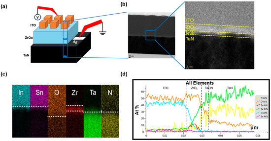
Figure 1.
(a) Schematic illustration of the device structure. (b) Typical cross-sectional transmission electron microscopy image of the ITO/ZrOx/TaN structure. (c) Energy dispersive X-ray spectroscopy (EDS) outcomes; colors represent In, Sn, O, Zr, Ta, and N. (d) EDS atomic percentage composition profiles.
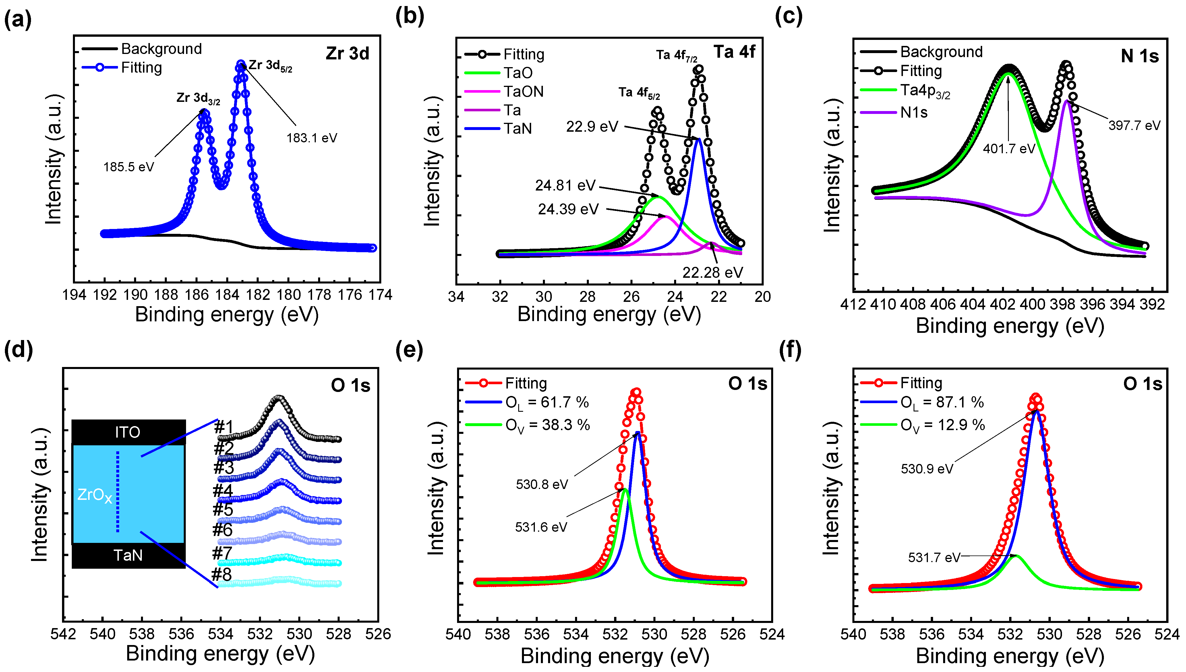
Figure 2 presents spectra obtained based on XPS analyses. The core-level spectra for Zr 3d and Ta 4f exhibit double spin–orbit splitting; specifically, Zr 3d3/2, Zr 3d5/2, Ta 4f5/2, and Ta 4f7/2. The background has been extracted using a modified Shirley method [30]. In Figure 2a, the spin–orbit splitting of Zr 3d is equal to 2.4 eV, and the peak differences in binding energy confirm this [31]. Similarly, in Figure 2b, the response has been fitted to detectable compounds, while the spin–orbit splitting of Ta 4f is 1.8 eV [32]. The binding energy peak at 24.39 eV corresponds to TaON, thus verifying the presence of the TaON interfacial layer in the XPS analysis [33]. In Figure 2c, the N 1s peak binding energy value of 397.7 eV implies Ta-N bonds [34]. Additional explanations for the remaining figures will be provided in subsequent sections.
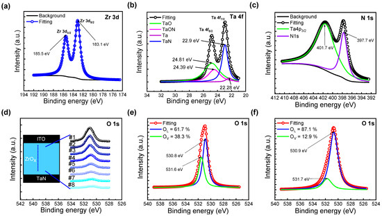
Figure 2.
X-ray photoelectron spectra of (a) Zr 3d, (b) Ta 4f, (c) N 1s. (d) O 1s spectra of the ZrOx layer at different etch times. (e) O 1s spectra obtained from ZrOx thin films #1 and (f) #8.
Figure 3a demonstrates the two different forming processes of fabricated ITO/ZrOx/TaN devices. In the case of SF, forming was performed in the voltage range of 0–5 V with a compliance current (CC) of 1 mA. Conversely, for DF, a two-step forming process was employed. In the first step, forming was performed when a bias of −7 V was applied with a CC of 1 mA. However, the current level decreases at the (2) state, thus indicating incomplete forming. In the second step, by applying a voltage bias of 3 V, the formation of a complete filament is presented. After the complete filament formation, the set and reset processes are induced by applying sequentially different polarity voltages. In Figure 3b, the device switches its resistance state in the SF case when the bias voltages of −2.5 V and 2.5 V are applied. As depicted, the variation during repeated cycles is significant, thus causing a gradual reduction in memory margin from the 1st to the 200th cycle. Conversely, in the case of DF, as illustrated in Figure 3c, the I–V curves for the 1st cycle and the 200th cycle match closely. Additionally, the operating voltage needed to induce resistive switching decreases to −1.5 V and 1.7 V, thus resulting in lower power consumption. Cycle-to-cycle endurance performance is illustrated in Figure 3d, where SF experiences a decrease in the HRS value over 200 cycles (read at −0.1 V), showing a large variance. In contrast, DF demonstrates stable switching over 200 cycles, thus maintaining a consistent resistance value. Furthermore, Figure 3e presents a box plot graph showing a uniform cell-to-cell performance in DF cells, presenting 20 DC cycles executed at 10 randomly selected ITO/ZrOx/TaN cells. The average ON/OFF ratio (RHRS/RLRS) of 5.624 indicates consistent performance. In Figure 3f, a retention test was conducted on the DF device to determine its lifetime. Findings demonstrate stable nonvolatile memory characteristics according to which the device maintains its resistance state for 104 s at a read voltage of −0.1 V.
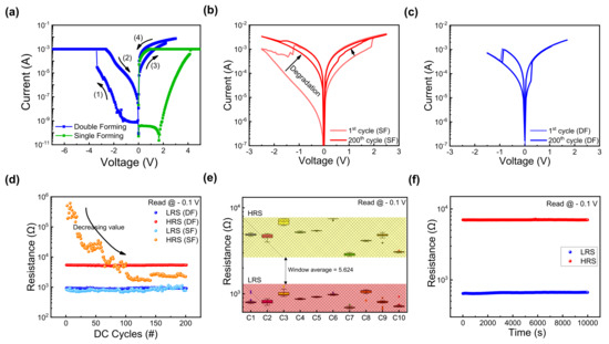
Figure 3.
(a) Double-forming (DF) process of ITO/ZrOx/TaN. (b) I–V curves of 1st and 200th cycles after single forming. (c) I–V curves of 1st and 200th cycles after double forming. (d) Endurance characteristics of ITO/ZrOx/TaN device under different forming processes for 200 direct current (DC) cycles. (e) Cell-to-cell uniformity of the DF device of 10 randomly selected cells. (f) Retention characteristics of the DF device.
In Figure 4a, the initial states of each layer and their alignment are depicted [35,36,37,38]. In the first step of DF, as illustrated in Figure 3a, when a negative voltage is applied to the top electrode, the ITO band state rises, thus creating a gradient. As this is a filamentary-type device, it allows electrons to hop through the ZrOx layer following the oxygen vacancies’ defect gradient, and to tunnel through the TaON barrier, thus leading to an increase in current, as shown in Figure 4b [39]. However, when the applied bias sweeps back to 0 V, the ITO band descends again and the TaON band flattens, thickening the barrier. Consequently, electrons cannot tunnel through, thus resulting in an incomplete filament formation and failure to form in a single step. This corresponds to the part of the I–V curve labeled as state (2) in Figure 2a during which the current decreases. To verify the FN tunneling phenomenon, the I–V curve is typically plotted as ln(I/V2) versus 1/V, as shown in Figure 4c [40]. Conversely, when a positive voltage is applied to the top electrode, the energy band diagram from TaN to ITO forms a stepped gradient, thus allowing electrons to be hopped in a single step. This explains why positive forming is a single-step process.
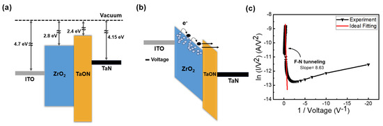
Figure 4.
Schematic of the conduction mechanism of the DF process of the ITO/ZrOx/TaN resistive random access memory. (a) Initial state. (b) First forming under negative bias application. (c) F-N tunneling curve fitting.
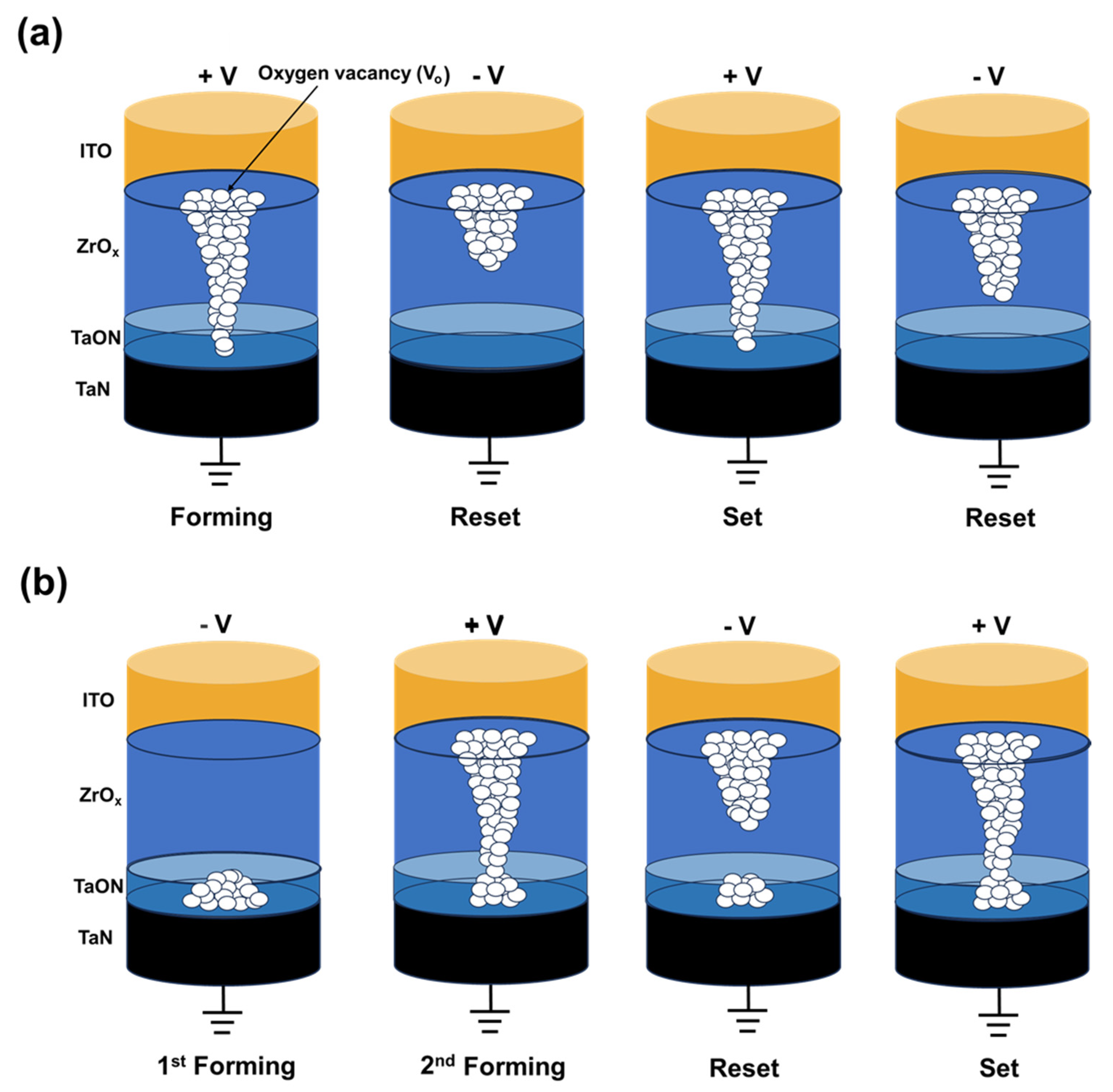
The mechanism of the two different forming processes is explained using a filament schematic in Figure 5. In contrast to DF, SF results in the formation of a complete filament in an SF step. To understand the reason for this, XPS etch times for O1s, detected along with Zr in Figure 2d, were divided into 8 intervals, with etch time #1 near the top electrode interface and etch time #8 near the bottom electrode interface; respective fitted outcomes are shown in Figure 2e,f. In Figure 2e, the area ratios of oxygen—in the form of O2− ions in the oxygen lattice (OL) and as defects, such as Vo2+ (oxygen vacancies)—were found to be 67.1% and 38.3%, respectively. In contrast, in Figure 2f, the respective ratios of oxygen-rich ZrOx and oxygen-deficient interfacial TaON layers were 87.1% and 12.9% [23].

Figure 5.
Schematic of the filament formation and rupture. (a) SF process. (b) DF process.
Based on the electrical and chemical characteristics of ITO/ZrOx/TaN, the conduction mechanism is proposed based on the migration of oxygen ions, as shown in Figure 5. In the case of the SF process (Figure 5a), when a positive bias is applied to the top electrode ITO, oxygen ions migrate toward the oxygen-reserving ITO electrode, thus leaving oxygen vacancies. Under continuous voltage stress, these vacancies accumulate and form a conducting filament, thus connecting the ITO and TaN electrodes. A large current flows through the conductive path, thus resulting in a resistance state change, from the initial resistance state (IRS) to an LRS. When an opposite bias is applied to the top electrode, the oxygen ions that migrate to the ITO electrode are repelled owing to the negative bias; correspondingly, they return to their original location. Through the migration of oxygen ions, recombination of oxygen ions and vacancies occurs, thus rupturing the conductive filament. However, during the repeatable switching, as shown in Figure 3d, degradation of device performance occurs in the SF mechanism. This may be owing to the inherent randomness of the conducting filament that results in different widths and the robustness of the conductive filament. Furthermore, the decreasing HRS of the SF device may be interpreted as the hard breakdown process occurring in the ZrOx film owing to the major voltage drop in this area [41].
Conversely, the mechanism of DF incorporates a two-step forming process to induce resistive switching phenomena in ITO/ZrOx/TaN devices. When a negative voltage is applied to the top electrode, oxygen ions migrate toward the TaN electrode, thus resulting in the breakdown of the TaON layer. However, during the process, the conductive filament is not completely formed (as in Figure 5b) owing to the insufficient CC [42]. When a positive bias is applied to the top electrode, oxygen ions migrate toward the ITO electrode, thus leaving oxygen vacancies and creating a conductive filament. This leads to an hourglass-shaped conductive path, with its weakest point located at the interface of ZrOx and TaON. Owing to this weak interface conductive filament, the RS phenomenon occurs in this area. This leads to uniform rupture and generation of conducting filaments, thus improving device-switching performance [43].
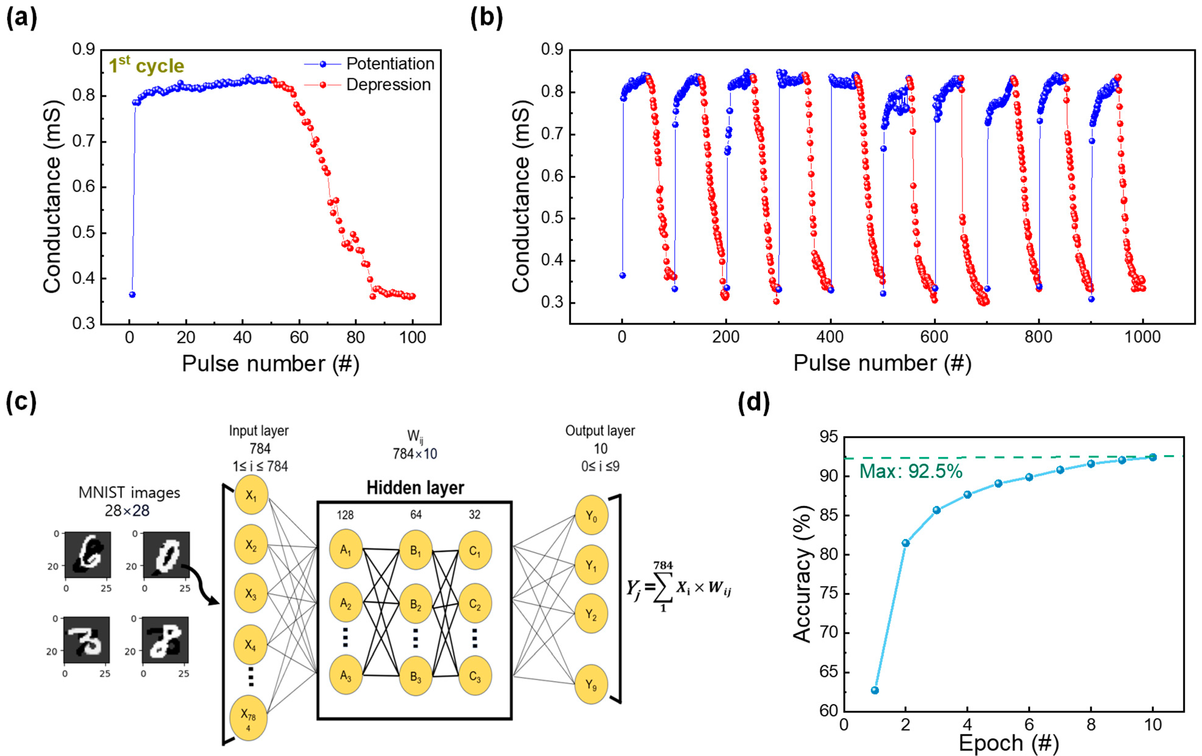
The uniform operation (occurring at low voltages) achieved based on the DF process is sufficient to utilize this RRAM device for neuromorphic applications. To confirm the synaptic characteristics, identical pulse tests were conducted (presented in Figure 6a). A voltage pulse (with an amplitude of 2.2 V and a width of 20 μs) was applied followed by a read voltage at 0.1 V to observe the change in conductance values; the process was repeated 50 times. Similarly, 50 consequent depression pulses were applied to decrease the conductance value of the device. The depression consisted of a reset pulse (amplitude and width of −2 V and 50 μs, respectively) also followed by a read pulse to observe a decrease in conductance value. Furthermore, the reproducibility of this behavior was tested by rehearsing this pulse application 10 times, as illustrated in Figure 6b [44]. Subsequently, the potentiation and depression curves of the ITO/ZrOx/TaN device were used (to extract weights) in a neural network for a pattern recognition system. The conductance values in Figure 6a were applied to , where Gmax and Gmin represent the maximum and minimum conductance values, respectively. Using this method, the conductance of potentiation and depression was converted into a 28 × 28-pixel handwritten number image based on MNIST, where the rise and fall of changes in conductance refer to the white and black pixels of the handwritten image. To conduct pattern recognition tests, a deep neural network that consisted of three layers of input, hidden, and output layers was used. Among the layers, the hidden layer was subdivided into an additional three layers, each having nodes of 128, 64, and 32, as depicted in Figure 6c. After training the machine learning model for 10 epochs and testing it with 10,000 images, it achieved an accuracy of 92.5%, as shown in Figure 6d.

Figure 6.
(a) Potentiation and depression curves of the ITO/ZrOx/TaN device. (b) Ten consecutive potentiation and depression cycles of ITO/ZrOx/TaN device. (c) Deep neural network simulation framework for modified National Institute of Standards and Technology (MNIST) pattern recognition. (d) Plot of pattern recognition accuracy of a synaptic device quantified at 10 epochs.
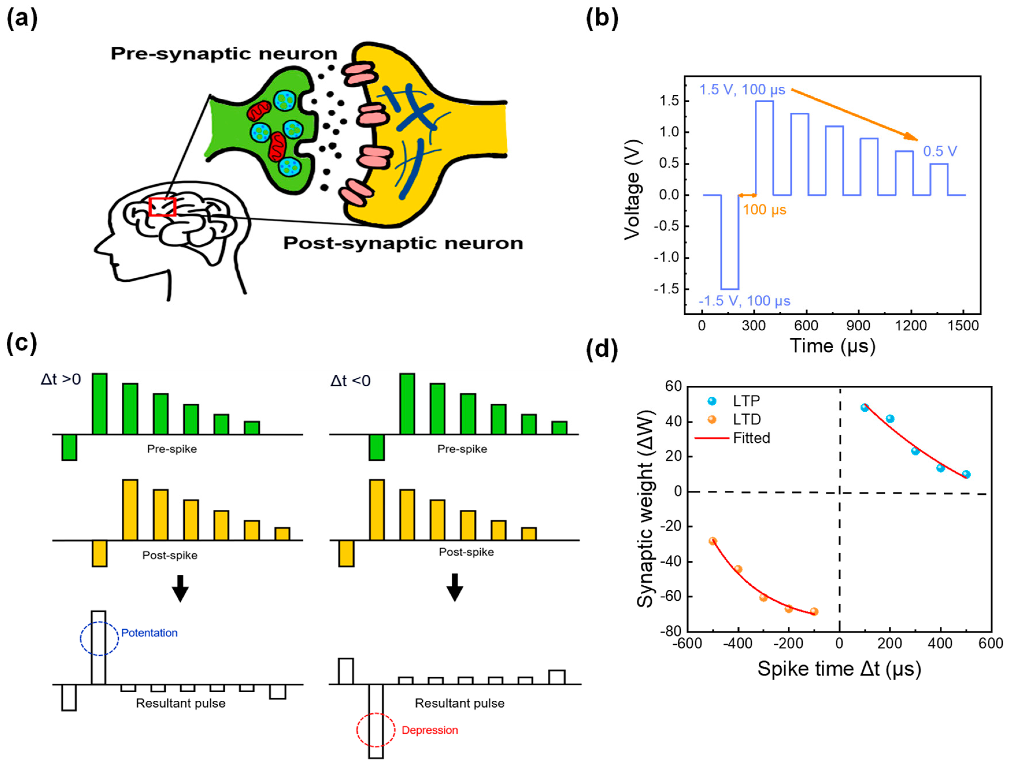
Finally, to implement and emulate synaptic responses, the Hebbian learning rule was applied to a neural network. One of the key features of the Hebbian learning rule is STDP. The STDP mechanism plays a crucial role in memory and learning in neural networks by regulating the connection strength of neurons. In the STDP mechanism, when presynaptic neurons receive stimuli, they transmit electrical signals known as spikes. When these spikes reach the synapse, neurotransmitters are released, thus activating the synapse. The postsynaptic neuronal receptors then detect this activity, and a spike is generated in the postsynaptic neuron after the synapse (that is, signal transmission occurs from presynaptic to postsynaptic neurons). This process is depicted in a simplified diagram in Figure 7a [45]. Owing to the simple two-terminal feature of the RRAM device, the biological synapse can be easily mimicked in the ITO/ZrOx/TaN device, where all pre- and postsynaptic parts are emulated by ITO and TaN layers as the top and bottom electrodes. To implement the fired spike and the time intervals of firing between pre- and postsynaptic regions, a pulse train shown in Figure 7b was applied to the top and the bottom electrodes at different time points. The pulse consisted of a pulse interval and width equal to 100 μs at the voltages of −1.5, 1.5, 1.3, 1.1, 0.9, 0.7, and 0.5 V [46]. At different time circumstances (spike time), the same pulses were applied to the top and bottom electrodes as those in Figure 7c. When the presynaptic spike amplitude exceeds that of the postsynaptic spike (Δt > 0), potentiation occurs, and the synaptic connections are strengthened. Conversely, when the postsynaptic spike exceeds the presynaptic spike amplitude (Δt < 0), depression occurs, and synaptic connections are inhibited. The term “spike time” refers to the difference in spike firing times of the pre-and postsynaptic regions (Δt = tpre − tpost). The resultant pulse, obtained by subtracting the postsynaptic from the presynaptic spike, was measured. When the interval time is shorter (that is, when the gap between spikes is smaller), it is perceived that there is a higher correlation between neurons, thus leading to significant changes in synaptic connections and transitioning into longer-term memory mechanisms. The result of the STDP function is illustrated in Figure 7d.
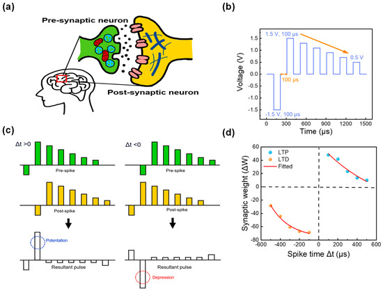
Figure 7.
(a) Schematic of human synaptic neural structure, (b) Pulse schematic, (c) Pulse authorization for spike-timing-dependent plasticity (STDP) measurements at Δt = 100 μs, (d) STDP measurement outcomes.
The term synaptic weight (ΔW) refers to the following equation:
where the terms Gf and Gi represent the values of conductance before and after pulse application. The fitted curve for the STDP function was obtained using the following equation:
where the terms A1, y0, and t1 are equal to 4.064, −76.569, and −2.007 × 10⁻⁴ for LTD, and 105.745, −40.356, and −6.382 × 10⁻⁴ for LTP, respectively. As illustrated by the results, gradual synaptic weight changes as a function of spike time can be observed following the STDP function.
4. Conclusions
In this study, we confirmed that the ITO/ZrOx/TaN RRAM device can form filaments using two different methods based on TEM and EDS line energy band diagrams and XPS analysis. Among these methods, the DF device exhibits lower current variation and low-power operation, thus making it more suitable for measuring synaptic characteristics in neuromorphic systems. First, we implemented pattern recognition for the MNIST dataset using identical pulses and machine learning. Second, we explored the applicability of this semiconductor as a neuromorphic chip mimicking the human brain. Based on STDP measurements, we observed varying degrees of long-term memory based on spike-time intervals, thus indicating its potential suitability as a long-term memory element in neuromorphic systems.
Author Contributions
M.K. (Minkang Kim) and D.J.: Formal analysis, Investigation, Writing—original draft. M.K. (Myounggon Kang) and S.K.: Writing—review and editing, Supervision, Resources, Project administration, Funding acquisition. All authors have read and agreed to the published version of the manuscript.
Funding
This research was supported by National R&D Program through the National Research Foundation of Korea (NRF) funded by Ministry of Science and ICT (2021M3F3A2A03017693), and was supported by Basic Science Research Program through the National Research Foundation of Korea (NRF) funded by the Ministry of Education (2018R1A6A1A03023788).
Data Availability Statement
Not applicable.
Conflicts of Interest
The authors declare that they have no known competing financial interest or personal relationship that could have appeared to influence the work reported in this paper.
References
- Avci, U.E.; Morris, D.H.; Young, I.A. Tunnel field-effect transistors: Prospects and challenges. IEEE J. Electron Device Soc. 2015, 3, 88–95. [Google Scholar] [CrossRef]
- Lonescu, A.M.; Riel, H. Tunnel field-effect transistors as energy-efficient electronic switches. Nature 2011, 479, 329–337. [Google Scholar] [CrossRef] [PubMed]
- Jeong, H.; Shi, L. Memristor devices for neural networks. J. Phys. D Appl. Phys. 2018, 52, 023003. [Google Scholar] [CrossRef]
- Pan, F.; Chen, C.; Wang, Z.; Yang, Y.; Yang, J.; Zeng, F. Nonvolatile resistive switching memories-characteristics, mechanisms and challenges. Prog. Nat. Sci. 2010, 20, 1–15. [Google Scholar] [CrossRef]
- Ou, Q.F.; Xiong, B.S.; Yu, L.; Wen, J.; Wang, L.; Tong, Y. In-Memory Logic Operations and Neuromorphic Computing in Non-Volatile Random Access Memory. Materials 2020, 13, 3532. [Google Scholar] [CrossRef] [PubMed]
- Tehrani, S.; Slaugther, J.M.; Chen, E.; Durlam, M.; Shi, J.; DeHerren, M. Progress and outlook for MRAM technology. IEEE Trans. Magn. 1999, 35, 2814–2819. [Google Scholar] [CrossRef]
- Sarwat, S.G. Materials science and engineering of phase change random access memory. Mater. Sci. Technol. 2017, 33, 1890–1906. [Google Scholar] [CrossRef]
- Takashima, D.; Kunishima, I. High-density chain ferroelectric random access memory (chain FRAM). IEEE J. Solid-State Circuit 1998, 33, 787–792. [Google Scholar] [CrossRef]
- Wang, Z.; Wu, H.; Burr, G.W.; Hwang, C.S.; Wang, K.L.; Xia, Q.; Yang, J.J. Resistive switching materials for information processing. Nat. Rev. Mater. 2020, 5, 173–195. [Google Scholar] [CrossRef]
- Marković, D.; Mizrahi, A.; Querlioz, D.; Grollier, J. Physics for neuromorphic computing. Nat. Rev. Phys. 2020, 2, 499–510. [Google Scholar] [CrossRef]
- Kim, K.M.; Jeong, D.S.; Hwang, C.S. Nanofilamentary resistive switching in binary oxide system; a review on the present status and outlook. Nanotechnology 2011, 22, 254002. [Google Scholar] [CrossRef] [PubMed]
- Li, Y.; Long, S.; Liu, Q.; Lv, H.; Liu, M. Resistive switching performance improvement via modulating nanoscale conductive filament, involving the application of two-dimensional layered materials. Small 2017, 13, 1604306. [Google Scholar] [CrossRef] [PubMed]
- Zahoor, F.; Zulkifli, T.Z.A.; Khanday, F.A. Resistive Random Access Memory (RRAM): An Overview of Materials, Switching Mechanism, Performance, Multilevel Cell (mlc) Storage, Modeling, and Applications. Nanoscale Res. Lett. 2020, 15, 90. [Google Scholar] [CrossRef] [PubMed]
- Yang, Y.; Lu, W.D. Progress in the characterizations and understanding of conducting filaments in resistive switching devices. IEEE Tans. Nanotechnol. 2016, 15, 465–472. [Google Scholar] [CrossRef]
- Lee, D.; Choi, H.; Sim, H.; Choi, D.; Hwang, H.; Lee, M.J.; Seo, S.A.; Yoo, I.K. Resistance switching of the nonstoichiometric zirconium oxide for nonvolatile memory applications. IEEE Electron Device Lett. 2005, 26, 719–721. [Google Scholar]
- Ju, D.; Kim, J.; Kim, S. Highly uniform resistive switching characteristics of Ti/TaOx/ITO memristor devices for neuromorphic system. J. Alloys Compd. 2023, 961, 170920. [Google Scholar] [CrossRef]
- Shen, Z.; Qi, Y.; Mitrovic, I.Z.; Zhao, C.; Hall, S.; Yang, L.; Luo, T.; Huang, Y.; Zhao, C. Effect of Annealing Temperature for Ni/AlOx/Pt RRAM Devices Fabricated with Solution-Based Dielectric. Micromachines 2019, 10, 446. [Google Scholar] [CrossRef]
- Cho, H.; Kim, S. Short-Term Memory Dynamics of TiN/Ti/TiO2/SiOx/Si Resistive Random Access Memory. Nanomaterials 2020, 10, 1821. [Google Scholar] [CrossRef]
- Ryu, H.; Kim, S. Effects of Oxygen Precursor on Resistive Switching Properties of CMOS Compatible HfO2-Based RRAM. Metals 2021, 11, 1350. [Google Scholar] [CrossRef]
- Smith, R.C.; Ma, T.; Hoilien, N.; Tsung, L.Y.; Bevan, M.J.; Colombo, L.; Roberts, J.; Campbell, S.A.; Gladfelter, W.L. Chemical vapour deposition of the oxides of titanium, zirconium and hafnium for use as high-k materials in microelectronic devices. A carbon-free precursor for the synthesis of hafnium dioxide. Adv. Mater. Opt. Electron. 2000, 10, 105–114. [Google Scholar] [CrossRef]
- Lin, C.Y.; Wu, C.Y.; Wu, C.Y.; Lee, T.C.; Yang, F.L.; Hu, C.; Tseng, T.Y. Effect of Top Electrode Material on Resistive Switching Properties of ZrO2 Film Memory Devices. IEEE Electron Device Lett. 2007, 28, 366–368. [Google Scholar] [CrossRef]
- Kim, C.; Lee, Y.; Kim, S.; Kang, M.; Kim, S. Diverse synaptic weight adjustment of bio-inspired ZrOx-based memristors for neuromorphic system. Mater. Sci. Semicond. Process. 2023, 157, 107314. [Google Scholar] [CrossRef]
- Huang, C.Y.; Huang, C.Y.; Tsai, T.L.; Lin, C.A.; Tseng, T.Y. Switching mechanism of double forming process phenomenon in ZrOx/HfOy bilayer resistive switching memory structure with large endurance. Appl. Phys. Lett. 2014, 104, 062901. [Google Scholar] [CrossRef]
- Zhang, Y.; Wang, C.; Wu, X. Review of electrical stimulus methods of in situ transmission electron microscope to study resistive random access memory. Nanoscale 2022, 14, 9542. [Google Scholar] [CrossRef] [PubMed]
- Proctor, A.; Sherwood, P.M.A. Data Analysis Techniques in X-ray Photoelectron Spectroscopy. Anal. Chem. 1982, 54, 13–19. [Google Scholar] [CrossRef]
- Strukov, D.B.; Kohlstedt, H. Resistive switching phenomena in thin films: Materials, devices, and applications. MRS Bull. 2012, 37, 108–114. [Google Scholar] [CrossRef]
- Cohen, G.; Afshar, S.; Tapson, J.; Schaik, A.V. EMNIST: Extending MNIST to handwritten letters. In Proceedings of the International Joint Conference on Neural Networks (IJCNN), Anchorage, AK, USA, 14–19 May 2017; pp. 2921–2926. [Google Scholar]
- Milo, V.; Lemini, D.; Chicca, E. Attractor networks and associative memories with STDP learning in RRAM synapses. In Proceedings of the IEEE International Electron Devices Meeting (IEDM), San Francisco, CA, USA, 2–6 December 2017; pp. 11.2.1–11.2.4. [Google Scholar]
- Li, C.; Hsieh, J.H. Experimental Investigation on the Sputtering Process for Tantalum Oxynitride Thin Films. Photonics 2021, 8, 53. [Google Scholar] [CrossRef]
- Matsumoto, R.; Nishizawa, Y.; Kataoka, N.; Tanaka, H.; Yoshikawa, H.; Tanuma, S.; Yoshihara, K. Reproducibility of XPS analysis for film thickness of SiO2/Si by active Shirley method. J. Electron Spectrosc. Relat. Phenom. 2016, 207, 55–59. [Google Scholar] [CrossRef]
- Kundu, S.; Halder, N.N.; Biswas, D.; Banerji, P.; Shripathi, T.; Chakraborty, S. Role of ultra thin pseudomorphic InP layer to improve the high-k dielectric/GaAs interface in realizing metal-oxide-semiconductor capacitor. J. Appl. Phys. 2012, 112, 034514. [Google Scholar] [CrossRef]
- Korkos, S.; Xanthopoulos, N.J.; Botzakaki, M.A.; Drivas, C.; Kennou, S.; Ladas, S.; Travlos, A.; Georga, S.N.; Krontiras, C.A. XPS analysis and electrical conduction mechanisms of atomic layer deposition grown Ta2O5 thin films onto p-Si substrates. J. Vac. Sci. Technol. 2020, 38, 032402. [Google Scholar] [CrossRef]
- Piallat, F.; Beugin, V.; Gassilloud, R.; Dussault, L.; Pelissier, B.; Leroux, C.; Caubet, P.; Vallée, C. Interface and plasma damage analysis of PEALD TaCN deposited on HfO2 for advanced CMOS studied by angle resolved XPS and C–V. Appl. Surf. Sci. 2014, 303, 388–392. [Google Scholar] [CrossRef]
- Zaman, A.; Meletis, E.I. Microstructure and mechanical properties of TaN thin films prepared by reactive magnetron sputtering. Coatings 2017, 7, 209. [Google Scholar] [CrossRef]
- Chia, J.Y.; Lertvanithphol, T.; Chaikeeree, T.; Seawsakul, K.; Thamrongsiripak, N.; Nakajima, H.; Songsiriritthigul, P.; Horprathum, M.; Nuntawong, N. Work function alteration of the porous indium tin oxide nanorods film by electron beam irradiation technique. Radiat. Phys. Chem. 2021, 188, 109664. [Google Scholar] [CrossRef]
- Dong, Y.F.; Wang, S.J.; Feng, Y.P.; Huan, A.C.H. Chemical tuning of band alignments for metal gate/high- oxide interfaces. Phys. Rev. B 2006, 73, 045302. [Google Scholar] [CrossRef]
- Fulton, C.C.; Lucovsky, G.; Nemanich, R.J. Electronic properties of the Zr–ZrO2–SiO2–Si (100) gate stack structure. J. Appl. Phys. 2006, 99, 063708. [Google Scholar] [CrossRef]
- Lahmer, M.A. Electronic structure, work function and band alignment of low Miller-index β-TaON surfaces; a DFT + U study. Comput. Condens. Matter 2023, 36, e00824. [Google Scholar] [CrossRef]
- Zhao, M.; Wu, H.; Gao, B.; Zhang, Q.; Wu, W.; Wang, S.; Xi, Y.; Wu, D.; Deng, N.; Yu, S.; et al. Investigation of statistical retention of filamentary analog RRAM for neuromophic computing. In Proceedings of the IEEE International Electron Devices Meeting (IEDM), San Francisco, CA, USA, 2–6 December 2017; pp. 39.4.1–39.4.4. [Google Scholar]
- Chand, U.; Huang, K.C.; Huang, C.Y.; Tseng, T.Y. Mechanism of Nonlinear Switching in HfO2-Based Crossbar RRAM With Inserting Large Bandgap Tunneling Barrier Layer. IEEE Trans. Electron Devices 2015, 62, 3665–3670. [Google Scholar] [CrossRef]
- Wang, Q.; Itoh, Y.; Tsuruoka, T.; Ohtsuka, S.; Shimizu, T.; Shingubara, S.; Hasegawa, T.; Aono, M. Dynamic moderation of an electric field using a SiO2 switching layer in TaOx -based ReRAM. Phys. Status Solidi-Rapid Res. Lett. 2015, 9, 166–170. [Google Scholar] [CrossRef]
- Tsai, T.L.; Chang, H.Y.; Lou, J.J.; Tseng, T.Y. A high performance transparent resistive switching memory made from ZrO2/AlON bilayer structure. Appl. Phys. Lett. 2016, 108, 153505. [Google Scholar] [CrossRef]
- Simanjuntak, F.M.; Panda, D.; Tsai, T.; Lin, C.; Wei, K.; Tseng, T. Enhanced switching uniformity in AZO/ZnO1−x/ITO transparent resistive memory devices by bipolar double forming. Appl. Phys. Lett. 2015, 107, 033505. [Google Scholar] [CrossRef]
- Woo, J.; Yu, S. Resistive Memory-Based Analog Synapse: The Pursuit for Linear and Symmetric Weight Update. IEEE Nanotechnol. Mag. 2018, 12, 36–44. [Google Scholar] [CrossRef]
- Caporale, N.; Dan, Y. Spike timing–dependent plasticity: A Hebbian learning rule. Annu. Rev. Neurosci. 2008, 31, 25–46. [Google Scholar] [CrossRef] [PubMed]
- Ryu, H.; Choi, J.; Kim, S. Voltage Amplitude-Controlled Synaptic Plasticity from Complementary Resistive Switching in Alloying HfOx with AlOx-Based RRAM. Metals 2020, 10, 1410. [Google Scholar] [CrossRef]


Disclaimer/Publisher’s Note: The statements, opinions and data contained in all publications are solely those of the individual author(s) and contributor(s) and not of MDPI and/or the editor(s). MDPI and/or the editor(s) disclaim responsibility for any injury to people or property resulting from any ideas, methods, instructions or products referred to in the content. |
© 2023 by the authors. Licensee MDPI, Basel, Switzerland. This article is an open access article distributed under the terms and conditions of the Creative Commons Attribution (CC BY) license (https://creativecommons.org/licenses/by/4.0/).