

Pixelated Filter Array for On-Chip Polarized Spectral Detection

 ,
, 
Abstract
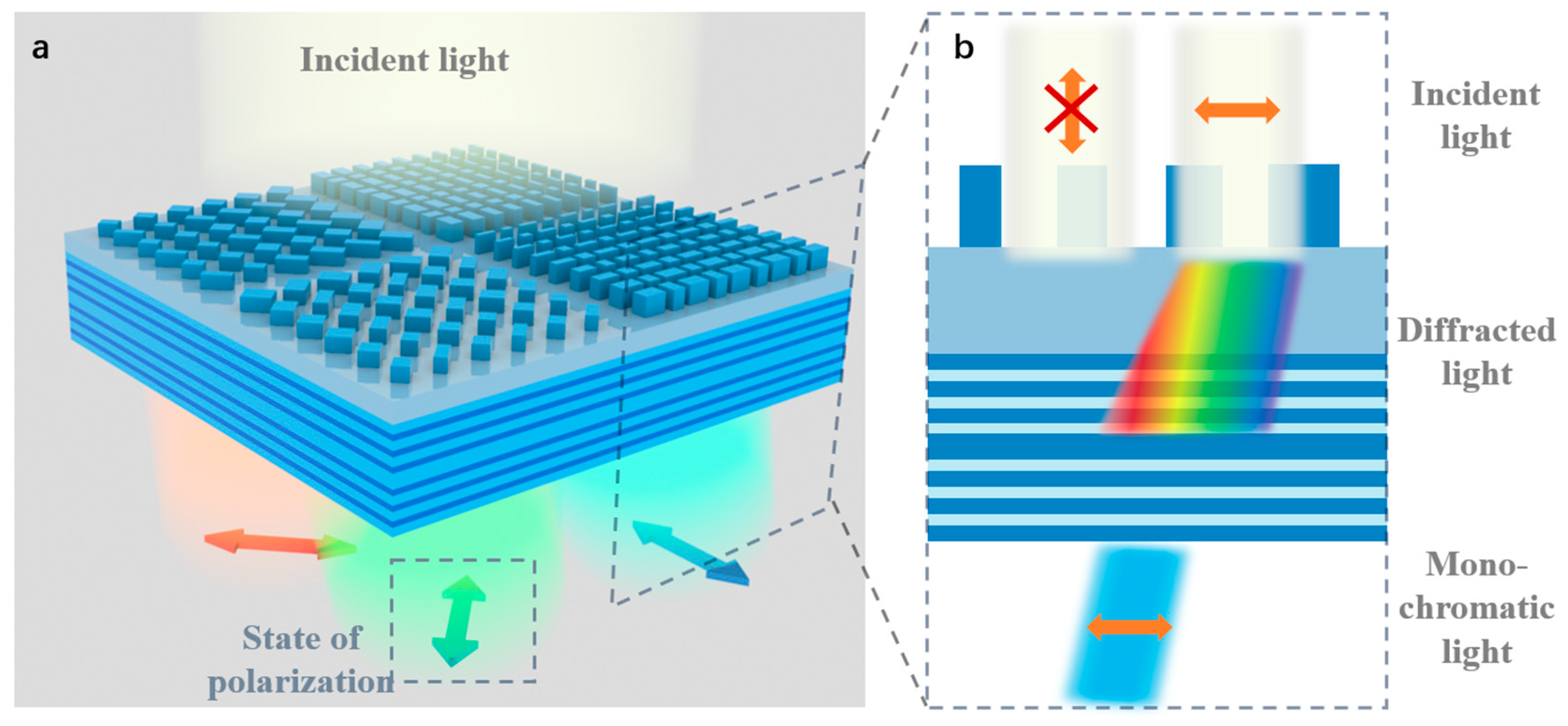
:1. Introduction
2. Theory and Simulation Result
2.1. Design of Polarization Selective Metasurface
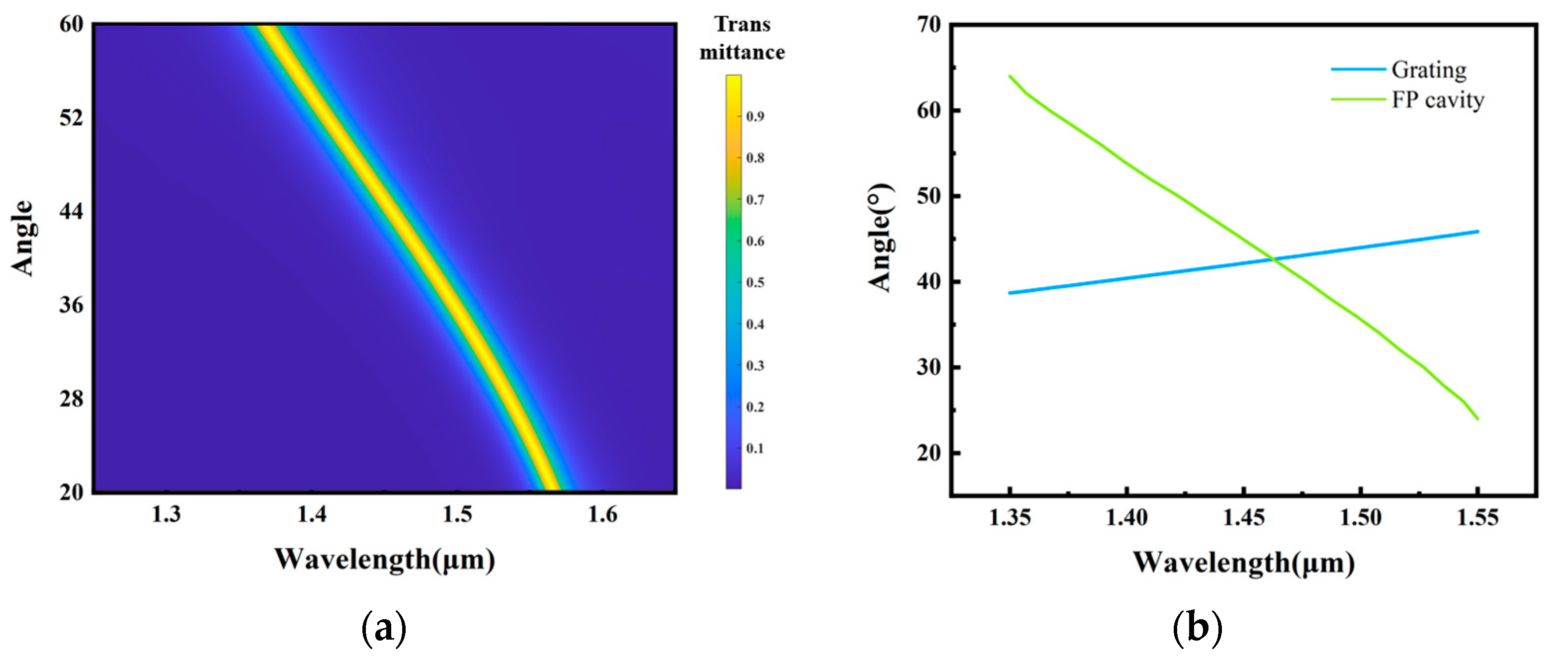
2.2. Design of Coupled Metasurface and FP Cavity
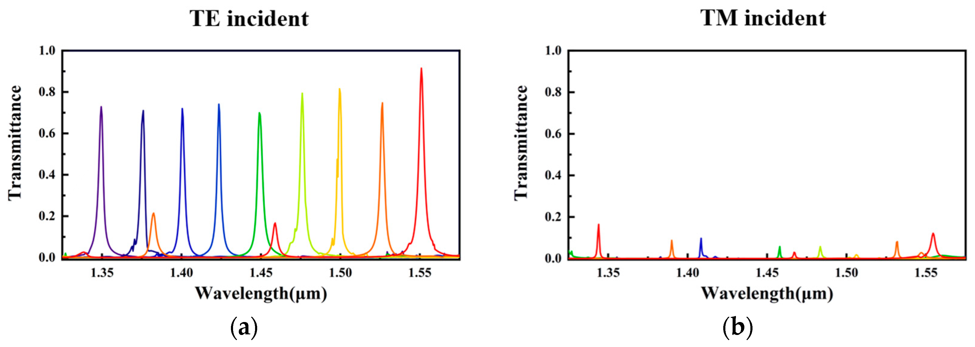
3. Discussion
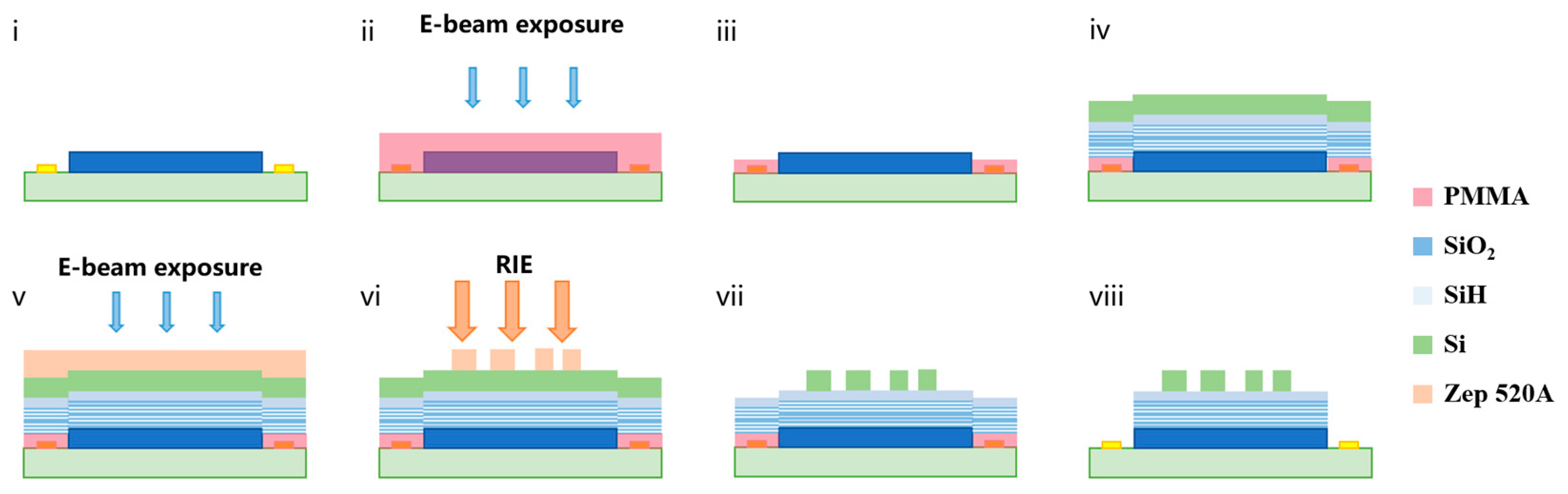
4. Fabrication Method
5. Conclusions
Author Contributions
Funding
Data Availability Statement
Conflicts of Interest
References
- Gupta, N. Acousto-Optic-Tunable-Filter-Based Spectropolarimetric Imagers for Medical Diagnostic Applications—Instrument Design Point of View. J. Biomed. Opt. 2005, 10, 051802. [Google Scholar] [CrossRef] [PubMed]
- Graham, L.; Yitzhaky, Y.; Abdulhalim, I. Classification of Skin Moles from Optical Spectropolarimetric Images: A Pilot Study. J. Biomed. Opt. 2013, 18, 111403. [Google Scholar] [CrossRef] [PubMed]
- Tyo, J.S.; Goldstein, D.L.; Chenault, D.B.; Shaw, J.A. Review of Passive Imaging Polarimetry for Remote Sensing Applications. Appl. Opt. 2006, 45, 5453. [Google Scholar] [CrossRef] [PubMed]
- Zhao, Y.; Zhang, L.; Zhang, D.; Pan, Q. Object Separation by Polarimetric and Spectral Imagery Fusion. Comput. Vis. Image Underst. 2009, 113, 855–866. [Google Scholar] [CrossRef]
- Van Harten, G.; De Boer, J.; Rietjens, J.H.H.; Di Noia, A.; Snik, F.; Volten, H.; Smit, J.M.; Hasekamp, O.P.; Henzing, J.S.; Keller, C.U. Atmospheric Aerosol Characterization with a Ground-Based SPEX Spectropolarimetric Instrument. Atmos. Meas. Tech. 2014, 7, 4341–4351. [Google Scholar] [CrossRef]
- Xu, J.-L.; Gobrecht, A.; Héran, D.; Gorretta, N.; Coque, M.; Gowen, A.A.; Bendoula, R.; Sun, D.-W. A Polarized Hyperspectral Imaging System for in Vivo Detection: Multiple Applications in Sunflower Leaf Analysis. Comput. Electron. Agric. 2019, 158, 258–270. [Google Scholar] [CrossRef]
- Li, S.; Jiao, J.; Wang, C. Research on Polarized Multi-Spectral System and Fusion Algorithm for Remote Sensing of Vegetation Status at Night. Remote Sens. 2021, 13, 3510. [Google Scholar] [CrossRef]
- Mohammadi Estakhri, N.; Edwards, B.; Engheta, N. Inverse-Designed Metastructures That Solve Equations. Science 2019, 363, 1333–1338. [Google Scholar] [CrossRef]
- Lalegani, Z.; Seyyed Ebrahimi, S.A.; Hamawandi, B.; La Spada, L.; Batili, H.; Toprak, M.S. Targeted Dielectric Coating of Silver Nanoparticles with Silica to Manipulate Optical Properties for Metasurface Applications. Mater. Chem. Phys. 2022, 287, 126250. [Google Scholar] [CrossRef]
- Pacheco-Peña, V.; Beruete, M.; Rodríguez-Ulibarri, P.; Engheta, N. On the performance of an ENZ-based sensor using transmission line theory and effective medium approach. New J. Phys. 2019, 21, 043056. [Google Scholar] [CrossRef]
- Akbari, M.; Shahbazzadeh, M.J.; La Spada, L.; Khajehzadeh, A. The Graphene Field Effect Transistor Modeling Based on an Optimized Ambipolar Virtual Source Model for DNA Detection. Appl. Sci. 2021, 11, 8114. [Google Scholar] [CrossRef]
- Greybush, N.J.; Pacheco-Peña, V.; Engheta, N.; Murray, C.B.; Kagan, C.R. Plasmonic Optical and Chiroptical Response of Self-Assembled Au Nanorod Equilateral Trimers. ACS Nano 2019, 13, acsnano.8b07619. [Google Scholar] [CrossRef] [PubMed]
- Lincoln, R.L.; Scarpa, F.; Ting, V.P.; Trask, R.S. Multifunctional Composites: A Metamaterial Perspective. Multifunct. Mater. 2019, 2, 043001. [Google Scholar] [CrossRef]
- Correia, J.H.; Bartek, M.; Wolffenbuttel, R.F. High-Selectivity Single-Chip Spectrometer for Operation at Visible Wavelengths. In Proceedings of the International Electron Devices Meeting 1998. Technical Digest (Cat. No.98CH36217); IEEE: San Francisco, CA, USA, 1998; pp. 467–470. [Google Scholar]
- Jayapala, M.; Lambrechts, A.; Tack, N.; Geelen, B.; Masschelein, B.; Soussan, P. Monolithic Integration of Flexible Spectral Filters with CMOS Image Sensors at Wafer Level for Low Cost Hyperspectral Imaging. In Proceedings of the 2023 International Image Sensor Workshop, Crieff Hydro Hotel, Crieff, UK, 21–25 May 2023. [Google Scholar]
- Genevet, P.; Capasso, F.; Aieta, F.; Khorasaninejad, M.; Devlin, R. Recent Advances in Planar Optics: From Plasmonic to Dielectric Metasurfaces. Optica 2017, 4, 139. [Google Scholar] [CrossRef]
- Bai, J.; Wang, C.; Chen, X.; Basiri, A.; Wang, C.; Yao, Y. Chip-Integrated Plasmonic Flat Optics for Mid-Infrared Full-Stokes Polarization Detection. Photonics Res. 2019, 7, 1051. [Google Scholar] [CrossRef]
- Yang, Z.; Albrow-Owen, T.; Cai, W.; Hasan, T. Miniaturization of Optical Spectrometers. Science 2021, 371, eabe0722. [Google Scholar] [CrossRef]
- McClung, A.; Samudrala, S.; Torfeh, M.; Mansouree, M.; Arbabi, A. Snapshot Spectral Imaging with Parallel Metasystems. Sci. Adv. 2020, 6, eabc7646. [Google Scholar] [CrossRef]
- Wang, Z.; Yi, S.; Chen, A.; Zhou, M.; Luk, T.S.; James, A.; Nogan, J.; Ross, W.; Joe, G.; Shahsafi, A.; et al. Single-Shot on-Chip Spectral Sensors Based on Photonic Crystal Slabs. Nat. Commun. 2019, 10, 1020. [Google Scholar] [CrossRef]
- Chen, W.T.; Török, P.; Foreman, M.R.; Liao, C.Y.; Tsai, W.-Y.; Wu, P.R.; Tsai, D.P. Integrated Plasmonic Metasurfaces for Spectropolarimetry. Nanotechnology 2016, 27, 224002. [Google Scholar] [CrossRef]
- Maguid, E.; Yulevich, I.; Veksler, D.; Kleiner, V.; Brongersma, M.L.; Hasman, E. Photonic Spin-Controlled Multifunctional Shared-Aperture Antenna Array. Science 2016, 352, 1202–1206. [Google Scholar] [CrossRef]
- Ding, F.; Pors, A.; Chen, Y.; Zenin, V.A.; Bozhevolnyi, S.I. Beam-Size-Invariant Spectropolarimeters Using Gap-Plasmon Metasurfaces. ACS Photonics 2017, 4, 943–949. [Google Scholar] [CrossRef]
- Maguid, E.; Yulevich, I.; Yannai, M.; Kleiner, V.; L Brongersma, M.; Hasman, E. Multifunctional Interleaved Geometric-Phase Dielectric Metasurfaces. Light Sci. Appl. 2017, 6, e17027. [Google Scholar] [CrossRef]
- Sun, T.; Hu, J.; Zhu, X.; Xu, F.; Wang, C. Broadband Single-Chip Full Stokes Polarization-Spectral Imaging Based on All-Dielectric Spatial Multiplexing Metalens. Laser Photonics Rev. 2022, 16, 2100650. [Google Scholar] [CrossRef]
- Xu, T.; Wu, Y.-K.; Luo, X.; Guo, L.J. Plasmonic Nanoresonators for High-Resolution Colour Filtering and Spectral Imaging. Nat. Commun. 2010, 1, 59. [Google Scholar] [CrossRef] [PubMed]
- Kaplan, A.F.; Xu, T.; Jay Guo, L. High Efficiency Resonance-Based Spectrum Filters with Tunable Transmission Bandwidth Fabricated Using Nanoimprint Lithography. Appl. Phys. Lett. 2011, 99, 143111. [Google Scholar] [CrossRef]
- Shyiq Amin, M.; Woong Yoon, J.; Magnusson, R. Optical Transmission Filters with Coexisting Guided-Mode Resonance and Rayleigh Anomaly. Appl. Phys. Lett. 2013, 103, 131106. [Google Scholar] [CrossRef]
- Wang, J.; Fan, Q.; Zhang, S.; Zhang, Z.; Zhang, H.; Liang, Y.; Cao, X.; Xu, T. Ultra-Thin Plasmonic Color Filters Incorporating Free-Standing Resonant Membrane Waveguides with High Transmission Efficiency. Appl. Phys. Lett. 2017, 110, 031110. [Google Scholar] [CrossRef]
- Pelzman, C.; Cho, S.-Y. Multispectral and Polarimetric Photodetection Using a Plasmonic Metasurface. J. Appl. Phys. 2018, 123, 043107. [Google Scholar] [CrossRef]
- Tu, X.; McEldowney, S.; Zou, Y.; Smith, M.; Guido, C.; Brock, N.; Miller, S.; Jiang, L.; Pau, S. Division of Focal Plane Red–Green–Blue Full-Stokes Imaging Polarimeter. Appl. Opt. 2020, 59, G33. [Google Scholar] [CrossRef]
- Jiang, S.; Li, J.; Li, J.; Lai, J.; Yi, F. Metamaterial Microbolometers for Multi-Spectral Infrared Polarization Imaging. Opt. Express 2022, 30, 9065. [Google Scholar] [CrossRef]
- Wang, S.-W.; Xia, C.; Chen, X.; Lu, W.; Li, M.; Wang, H.; Zheng, W.; Zhang, T. Concept of a High-Resolution Miniature Spectrometer Using an Integrated Filter Array. Opt. Lett. 2007, 32, 632. [Google Scholar] [CrossRef] [PubMed]
- Wang, S.-W.; Li, M.; Xia, C.-S.; Wang, H.-Q.; Chen, X.-S.; Lu, W. 128 Channels of Integrated Filter Array Rapidly Fabricated by Using the Combinatorial Deposition Technique. Appl. Phys. B 2007, 88, 281–284. [Google Scholar] [CrossRef]
- Shaltout, A.M.; Kim, J.; Boltasseva, A.; Shalaev, V.M.; Kildishev, A.V. Ultrathin and Multicolour Optical Cavities with Embedded Metasurfaces. Nat. Commun. 2018, 9, 2673. [Google Scholar] [CrossRef] [PubMed]
- Saxe, S.; Sun, L.; Smith, V.; Meysing, D.; Hsiung, C.; Houck, A.; Von Gunten, M.; Hruska, C.; Martin, D.; Bradley, R.; et al. Advances in Miniaturized Spectral Sensors. In Proceedings of the Next-Generation Spectroscopic Technologies XI; Druy, M.A., Crocombe, R.A., Barnett, S.M., Profeta, L.T., Azad, A.K., Eds.; SPIE: Orlando, FL, USA, 2018; p. 10. [Google Scholar]
- Lerose, D.; Siaw Hei, E.K.; Ching, B.C.; Sterger, M.; Yaw, L.C.; Schulze, F.M.; Schmidt, F.; Schmidt, A.; Bach, K. CMOS-Integrated Geometrically Tunable Optical Filters. Appl. Opt. 2013, 52, 1655. [Google Scholar] [CrossRef]
- Geelen, B.; Tack, N.; Lambrechts, A. A Compact Snapshot Multispectral Imager with A Monolithically Integrated Per-Pixel Filter Mosaic; von Freymann, G., Schoenfeld, W.V., Rumpf, R.C., Eds.; SPIE: San Francisco, CA, USA, 2014; p. 89740L. [Google Scholar]
- Horie, Y.; Arbabi, A.; Arbabi, E.; Kamali, S.M.; Faraon, A. Wide Bandwidth and High Resolution Planar Filter Array Based on DBR-Metasurface-DBR Structures. Opt. Express 2016, 24, 11677. [Google Scholar] [CrossRef]
- Pjotr Stoevelaar, L.; Berzinš, J.; Silvestri, F.; Fasold, S.; Kamali, K.Z.; Knopf, H.; Eilenberger, F.; Setzpfandt, F.; Pertsch, T.; Bäumer, S.M.B.; et al. Nanostructure-Modulated Planar High Spectral Resolution Spectro-Polarimeter. Opt. Express 2020, 28, 19818. [Google Scholar] [CrossRef]
- Arbabi, A.; Horie, Y.; Bagheri, M.; Faraon, A. Dielectric Metasurfaces for Complete Control of Phase and Polarization with Subwavelength Spatial Resolution and High Transmission. Nat. Nanotechnol. 2015, 10, 937–943. [Google Scholar] [CrossRef]
- Balthasar Mueller, J.P.; Rubin, N.A.; Devlin, R.C.; Groever, B.; Capasso, F. Metasurface Polarization Optics: Independent Phase Control of Arbitrary Orthogonal States of Polarization. Phys. Rev. Lett. 2017, 118, 113901. [Google Scholar] [CrossRef]
- Fan, Q.; Liu, M.; Zhang, C.; Zhu, W.; Wang, Y.; Lin, P.; Yan, F.; Chen, L.; Lezec, H.J.; Lu, Y.; et al. Independent Amplitude Control of Arbitrary Orthogonal States of Polarization via Dielectric Metasurfaces. Phys. Rev. Lett. 2020, 125, 267402. [Google Scholar] [CrossRef]
- Liu, M.; Zhu, W.; Huo, P.; Feng, L.; Song, M.; Zhang, C.; Chen, L.; Lezec, H.J.; Lu, Y.; Agrawal, A.; et al. Multifunctional Metasurfaces Enabled by Simultaneous and Independent Control of Phase and Amplitude for Orthogonal Polarization States. Light Sci. Appl. 2021, 10, 107. [Google Scholar] [CrossRef]
- Feng, C.; He, T.; Shi, Y.; Song, Q.; Zhu, J.; Zhang, J.; Wang, Z.; Tsai, D.P.; Cheng, X. Diatomic Metasurface for Efficient Six-Channel Modulation of Jones Matrix. Laser Photonics Rev. 2023, 17, 2200955. [Google Scholar] [CrossRef]

Disclaimer/Publisher’s Note: The statements, opinions and data contained in all publications are solely those of the individual author(s) and contributor(s) and not of MDPI and/or the editor(s). MDPI and/or the editor(s) disclaim responsibility for any injury to people or property resulting from any ideas, methods, instructions or products referred to in the content. |
© 2023 by the authors. Licensee MDPI, Basel, Switzerland. This article is an open access article distributed under the terms and conditions of the Creative Commons Attribution (CC BY) license (https://creativecommons.org/licenses/by/4.0/).
Share and Cite
Liu, Y.; Feng, C.; Dong, S.; Zhu, J.; Wang, Z.; Cheng, X. Pixelated Filter Array for On-Chip Polarized Spectral Detection. Nanomaterials 2023, 13, 2624. https://doi.org/10.3390/nano13192624
Liu Y, Feng C, Dong S, Zhu J, Wang Z, Cheng X. Pixelated Filter Array for On-Chip Polarized Spectral Detection. Nanomaterials. 2023; 13(19):2624. https://doi.org/10.3390/nano13192624
Chicago/Turabian StyleLiu, Yuechen, Chao Feng, Siyu Dong, Jingyuan Zhu, Zhanshan Wang, and Xinbin Cheng. 2023. "Pixelated Filter Array for On-Chip Polarized Spectral Detection" Nanomaterials 13, no. 19: 2624. https://doi.org/10.3390/nano13192624
APA StyleLiu, Y., Feng, C., Dong, S., Zhu, J., Wang, Z., & Cheng, X. (2023). Pixelated Filter Array for On-Chip Polarized Spectral Detection. Nanomaterials, 13(19), 2624. https://doi.org/10.3390/nano13192624