Article

Cs2TiI6 (Cs2TiIxBr6-x) Halide Perovskite Solar Cell and Its Point Defect Analysis

by
Sadia Sultana Urmi
1,
Md Abdul Kaium Khan
2,*,
Tasnim Tareq Ferdous
1,
Davoud Adinehloo
2,
Vasili Perebeinos
2 and
Mohammad Abdul Alim
1
1
Department of Electrical & Electronic Engineering, University of Chittagong, Chittagong 4331, Bangladesh
2
Department of Electrical Engineering, University at Buffalo, The State University of New York, Buffalo, NY 14260, USA
*
Author to whom correspondence should be addressed.
Nanomaterials 2023, 13(14), 2100; https://doi.org/10.3390/nano13142100
Submission received: 20 June 2023 / Revised: 13 July 2023 / Accepted: 17 July 2023 / Published: 19 July 2023
(This article belongs to the Section Solar Energy and Solar Cells)

Abstract

:
This work presents a comprehensive numerical study for designing a lead-free, all-inorganic, and high-performance solar cell based on Cs2TiI6 halide perovskite with all-inorganic carrier transport layers. A rigorous ab initio density-functional theory (DFT) calculation is performed to identify the electronic and optical properties of Cs2TiI6 and, upon extraction of the existing experimental data of the material, the cell is designed and optimized to the degree of practical feasibility. Consequently, a theoretical power conversion efficiency (PCE) of 21.17% is reported with inorganic TiO2 and CuI as carrier transport layers. The calculated absorption coefficient of Cs2TiI6 reveals its enormous potential as an alternative low-bandgap material for different solar cell applications. Furthermore, the role of different point defects and the corresponding defect densities on cell performance are investigated. It is found that the possible point defects in Cs2TiI6 can form both the shallow and deep defect states, with deep defect states having a prominent effect on cell performance. For both defect states, the cell performance deteriorates significantly as the defect density increases, which signifies the importance of high-quality material processing for the success of Cs2TiI6-based perovskite solar cell technology.

1. Introduction

Perovskite solar cell (PSC) technology is promising a breakthrough in the solar cell industry with the potential for thin-film processing, flexibility, and low-cost commercialization due to the simple solution process used in the chemical preparation of the perovskites [1,2,3]. The lead-based halide perovskites, e.g., methylammonium lead halide (MAPbX3) and formamidinium lead halide (FAPbX3), have already exceeded the recorded power conversion efficiencies of CIGS and CdTe-based solar cells [4] and, recently, a FAPbI3 perovskite solar cell has obtained a record power conversion efficiency (PCE) of 25.6% [5]. On the other hand, a PCE of 26.3% ± 0.5% hysteresis [6] was reported for silicon-based solar cells. As a result, perovskite solar cell technology will soon possess the potential to become a serious competitor of the well-established silicon-based solar cell technology. Presently, perovskite solar cells with higher efficiencies are mainly lead (Pb)-based due to the excellent optoelectronic properties like high carrier mobilities, long carrier lifetimes, high absorption coefficients, and direct bandgaps [7,8,9,10,11]. However, the higher efficiencies are accompanied by serious drawbacks like the toxicity of lead, reduction in the perovskite compound shelf life, and the unstable nature of device performance due to the hygroscopic and volatile organic cations [12,13,14,15]. Therefore, finding a suitable alternative for the lead (Pb)-based halide perovskites has become necessary, and extensive research is ongoing to find new perovskite materials that might yield the same high PCE or even better. Recent studies show that MA+ and FA+ can be replaced by Cs+ cation, leading to enhanced thermal and moisture stability [16]. Also, the toxic Pb2+ can be replaced by non-toxic cations like Bi3+, Ag+, Ge2+, Sn2+, In+, and Sb3+ [17,18,19]. However, the proposed lead-free perovskites suffer from very low power conversion efficiencies. In one study [17], a fabricated Cs2AgBiBr6-based perovskite solar cell could only reach an efficiency of 2.43% due to the high bandgap of the perovskite, which restricted further performance enhancement. Similar performance was observed in another [20], where an efficiency of 2.23% was achieved for the same perovskite. In a study by Chen et al. [21], the authors presented a CsSnGeI3-based solar cell with up to 7.11% efficiency. In another study [22], a CsSnI3-based solar cell achieved 6.08% efficiency, and in another [23], an efficiency of 7.5% was achieved with the incorporation of N, N′-methylenebis(acrylamide) (MBAA) with CsSnI3. However, the metallic conductivity of CsSnI3 seriously restricts the development of the solar cell [24,25], and Sn2+ being highly sensitive to ambient moisture and oxygen [24] makes it difficult to prevent the degradation of the solar cell.
In recent times, a new series of Ti-based lead-free vacancy-ordered halide double perovskite was proposed by Ju et al. [26] with a chemical formulation of Cs2TiIxBr6-x (x = 0, 2, 4, 6). The bandgap tunability (~1.02 to ~1.78 eV) of this particular type of perovskite and the stable and nontoxic nature of Ti make them an ideal candidate for highly stable and environment-friendly single-junction as well as tandem solar cell applications. Until now, most studies have been conducted on solar cells based on Cs2TiBr6 (Cs2TiIxBr6-x; x = 0). Chen et al. [27] fabricated a Cs2TiBr6-based solar cell for the first time with an absorbing Cs2TiBr6 layer thickness of ~200 nm. They reported a bandgap of ~1.8 eV, consistent with the previous report [26], and the carrier-diffusion length was more than 100 nm. The solar cell exhibited high stability and the sustainability of high thermal stress in ambient conditions. However, the fabricated PSC could only achieve a stable PCE of 2.15%, which was increased to 3.22% by incorporating a C60 layer. To increase the PCE, a few numerical studies have been carried out [28,29,30,31,32,33,34,35,36], where different carrier transport materials were proposed for better device performance.
In the case of Cs2TiI6 (Cs2TiIxBr6-x; x = 6)-based solar cells, the number of studies is very limited and most of the studies lack consistency with experimental data. Previously, in one study [37], a PCE of 15.06% was reported for a Cs2TiI6 PSC with CdTe as the hole transport layer (HTL), and in another [38], a PCE of 16.31% was reported with CuSCN as HTL. However, the used bandgaps of Cs2TiI6 for these two numerical simulations are vastly inconsistent with the measured bandgap of ~1.02 eV [26], and the proposed absorber defect densities will be hard to achieve experimentally. Recently, Zhao et al. [39] provided a numerical study on Cs2TiI6 for solar cell and alpha-particle detection applications with organic PEDOT:PSS and C60 as carrier transport layers. They found high retainability of PCE after a very high proton fluence level and reported a PCE of 22.7% for single-junction and 26.78% for tandem solar cells. However, the high numerical PCE level was achieved for a very low defect density (1010 cm−3) of the Cs2TiI6 absorbing layer, which might be very difficult to replicate in practice because, for this family of material, the defect density level can be found in the region of 1014 to 1016 cm−3 and it was close to ~1015 cm−3 for the fabricated Cs2TiBr6 PSC [27,35]. Also, their simulated output of 22.7% PCE is for abnormally high electron mobility (μn = 2.26 × 104 cm2/Vs) and hole mobility (μp = 7.38 × 103 cm2/Vs), which the authors declare as an ideal case. However, these values are multiple orders of magnitude higher than what was found in practice for the same family of perovskite [27,35]. Therefore, this calls for a further investigation into the possible utilization of Cs2TiI6 as an active layer in PSCs considering the practical realizability of the device itself, and it includes making a proper choice of the carrier transport layers to maximize cell performance, even with the relatively higher defect density found in this family of perovskites. Also, Cs2TiI6-based perovskite solar cells with all-inorganic charge transport materials can be explored due to the low cost, excellent physicochemical stability, and proper photovoltaic properties of the inorganic charge transport materials [40,41]. Although the effects of different point defects on the performance of relatively high bandgap Cs2TiBr6-based PSC has been studied previously [35], there is no detailed report for the low-bandgap Cs2TiI6-based PSC. Therefore, additional insight into the existing point defects in Cs2TiI6, and the overall impact of the possible shallow and deep defect states on the performance of Cs2TiI6-based PSC, can aid experimentalists in fine-tuning material processing prior to device fabrication.
This article proposes a novel lead-free Cs2TiI6 PSC with all-inorganic carrier transport materials and an n-i-p type FTO/TiO2/Cs2TiI6/CuI/Au structure. At first, a first principles density-functional theory (DFT) calculation is performed to evaluate the electrical and optical properties of Cs2TiI6 and its suitability in PSC applications. Then, the device is designed using experimentally extracted data and optimized to the degree of practical feasibility. Furthermore, we analyze the impacts of existing point defects in Cs2TiI6, and their charge transition levels on the device performance and find the keys to designing highly efficient Cs2TiI6 PSCs. We also discuss the morphological features of the material and potential ways to achieve high-quality thin films and consequently realize the full potential of the material for PSC applications. Our results demonstrate valuable insights into PSC performance, and we believe the study can accelerate/aid the practical implementation and testing of highly efficient Cs2TiI6 PSCs for different real-world applications.

2. Ab Initio DFT Calculation and Cell Modeling

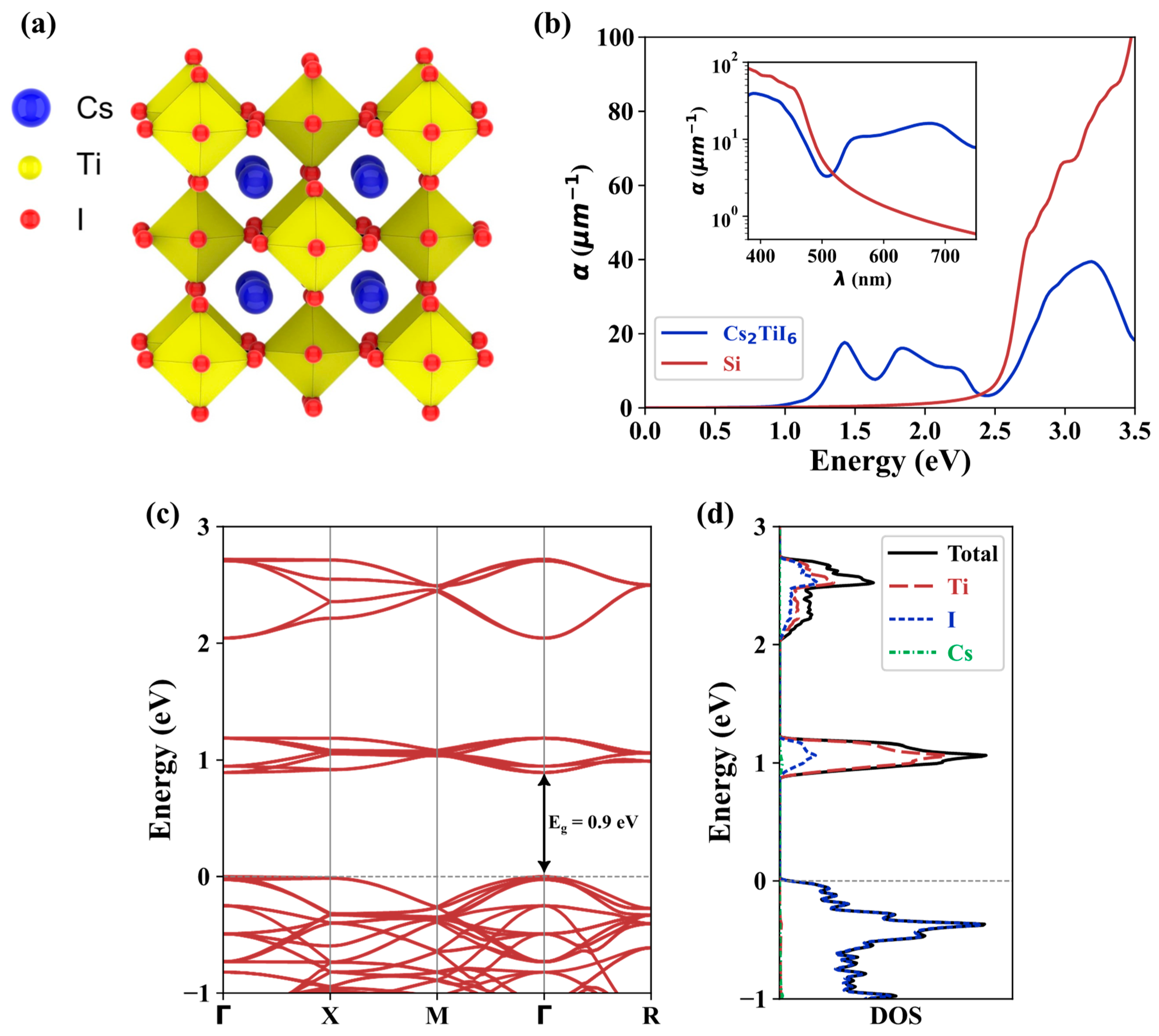
2.1. First Principles Calculation of Cs2TiI6 Perovskite

The electronic properties of Cs2TiI6 were calculated using the first principles DFT framework implemented in the open-source code Quantum Espresso [42]. Norm-conserving PBE pseudopotentials [43] were utilized, and the cutoff energy was set to 100 Ry. Brillouin zone sampling used an 11 × 11 × 11 k-mesh. A schematic of the crystal structure of Cs2TiI6 is shown in Figure 1a. The atomic positions were relaxed to obtain the maximum force < 0.005 eV/ on each atom, yielding a lattice constant of 11.829 . The band structure of the crystal is depicted in Figure 1c. A direct bandgap of 0.9 eV was observed at the Γ point, which is slightly lower than the experimental value of ~1.02 eV [26]. However, it is worth noting that PBE is known to underestimate the bandgap, which has contributed to this discrepancy [44,45]. Also, a similar discrepancy was found for the DFT calculation of Cs2TiBr6 using PBE (Eg ~ 1.5 eV) and its experimental bandgap value (Eg ~ 1.8 eV) [27]. Figure 1d shows the density of states (DOS) and the projected DOS of Cs2TiI6. The analysis reveals that the orbitals of Ti and I atoms mainly contributed to the conduction band’s lowest energy states and the valence band’s highest energy states. Notably, the DOS of Cs atoms did not exhibit significant contributions in these energy ranges.
Optical absorption properties were essential in evaluating the suitability of materials for photovoltaic applications. The optical absorption coefficient can be determined through the calculation of the dielectric function using Equation (1) [46]:
α ω = ω ε 2 n c = 2 ω c ε 1 2 + ε 2 2 ε 1 1 2
where ω is the frequency of the incident light, c is the speed of light, n is the refractive index, and ε 1 and ε 2 are the real and imaginary parts of the dielectric function, respectively. Silicon (Si), a low bandgap material, has been the conventional material of choice for photovoltaic applications. Figure 1b shows the calculated absorption coefficient of Cs2TiI6 and Si. For lower photon energies, Cs2TiI6 possesses a promising optical absorption and should be able to absorb light with wavelengths beyond the visible spectrum. Also, in the visible spectrum [inset of Figure 1b], Cs2TiI6 showed a promising absorption for longer wavelengths. A possible implication is that Cs2TiI6 can be used as the bottom cell in tandem solar cell structures, where Si or other lead-based or organic perovskites currently find application. Thus, Cs2TiI6 has the potential to be an alternative material for highly efficient, lead-free, all-inorganic perovskite–perovskite tandem solar cell technology.

2.2. Cs2TiI6 Perovskite Solar Cell

We utilized the widely known Solar Cell Capacitance Simulator (SCAPS-1D 3.3.07) software developed by the Department of Electronics and Information Systems (ELIS), University of Gent, Belgium [47,48,49]. Section S1 of the Supplementary Information discusses the numerical techniques and Poisson’s equations used in SCAPS-1D. The section also discusses mathematical equations to derive other important material parameters to design solar cells in SCAPS-1D.
In Section S2 of the Supplementary Information, we validated the simulation tool’s accuracy and the reliability of the meticulously chosen device parameters by replicating the performance of an existing fabricated device of the same Cs2TiIxBr6-x family. This provided the required credibility to the numerical setup as well as the numerically predicted device performance.
Figure 2a is the graphical representation of different layers of the proposed device, and Figure 2b shows the corresponding energy levels. Table 1 provides the material parameters and their values used for the device modeling. The parameter values were chosen meticulously from various sources, and emphasis was given to experimentally derived data in order to design a practically realizable device. The hole transport layer (HTL) and electron transport layer (ETL) thicknesses were chosen carefully to ensure adequate light transmission through FTO onto the absorber layer. Where a thick layer might prevent enough light transmission and generation of adequate electron-hole pairs, a very thin layer might create a leakage path due to various voids and pinholes created during thin film processing, and the device would possess poor stability due to some chemisorbed hydroxides [50].
To create a more realistic device, we applied defects in all the layers as well as in the absorber/carrier transport layer interfaces, as provided in Tables S2 and S3 of the supplementary Information. Figure 3 shows the current density (J) versus the voltage (V) output, and Figure 4 depicts the quantum efficiency (QE) versus the wavelength curve. For a high absorber defect density of 4.16 × 1015 cm−3, the device still possessed a decent PCE of 7.07% with an average quantum efficiency of ~30% for the visible spectrum. The relatively improved device performance compared to Cs2TiBr6 [27] can be attributed to the choice of hole transport material, with CuI having a very small valence band offset of ~0.18 eV and good carrier mobility that allows proper extraction and transportation of holes from the perovskite to the anode. Also, the low bandgap of Cs2TiI6 aids the creation of electron–hole pairs as it can absorb photon energy in a wide spectrum and leads to a high current density of the device. The overall impact of different inorganic hole transport layer (HTL) materials on the device’s performance is described in Section S3 of the Supplementary Information.

3. Cell Optimization

The proposed solar cell with existing experimentally derived parameters has already provided us with promising results. Therefore, it is necessary to extend the study further and ascertain the optimum device parameters within practically feasible limits in order to propose an optimized device to aid the experimental realization of Cs2TiI6-based perovskite solar cells.

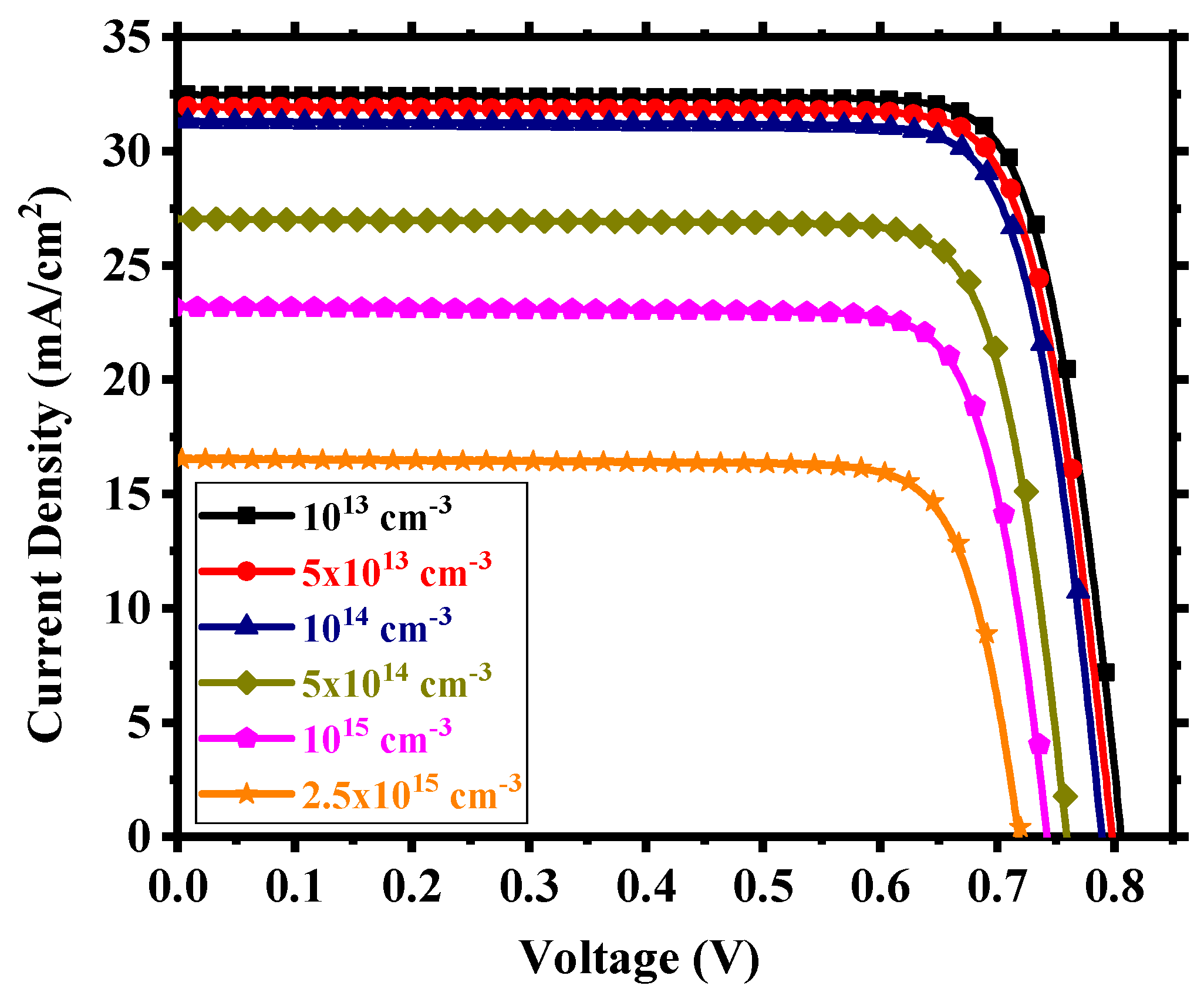
3.1. Optimization of Defect Density

We considered interfacial defects at the electron transport layer (ETL)/absorbing perovskite and absorbing perovskite/hole transport layer (HTL) interfaces as well as defects within the perovskite. The defect density within these regions is crucial for device performance. We studied the device for an interfacial defect density in the range of 1010 to 1014 cm−2. Figure 5 shows the corresponding J-V performance. Above 1012 cm−2, the effect of interfacial defect density became prominent with performance degradation and, below this, there was little to no change in output. The decline in performance can be attributed to the increase in the number of traps at the recombination centers [56]. For a defect density of 1012 cm−2, the device possessed power conversion efficiency (PCE) of 7.35%, fill factor (FF) of 81.25%, open-circuit voltage (Voc) of 0.706 V, and short-circuit current density (Jsc) of 12.82 mA/cm2. With an optimum interfacial defect density of 1012 cm−2, we studied the effect of absorbing perovskite’s (Cs2TiI6) defect density in the range of 1013 to 2.5 × 1015 cm−3. It is quite clear from Figure 6 that the device performance relied heavily on the absorber defect density, and it was crucial to maintain an optimum defect density of this layer to achieve a high-performance PSC. Above 1014 cm−3, the device started to underperform with deterioration in performance due to the sudden expansion of recombination rate within the absorber layer [57] and, below 1014 cm−3, there was an enhancement in performance but not a substantial one. Also, we need to keep in mind the practical feasibility of achieving a certain defect profile. All aspects considered, we thus chose an absorber defect density of 1014 cm−3 as an optimum value and, with this defect profile, the device possessed Jsc of 31.31 mA/cm2, Voc of 0.79 V, FF of 81.59%, and PCE of 20.22%.

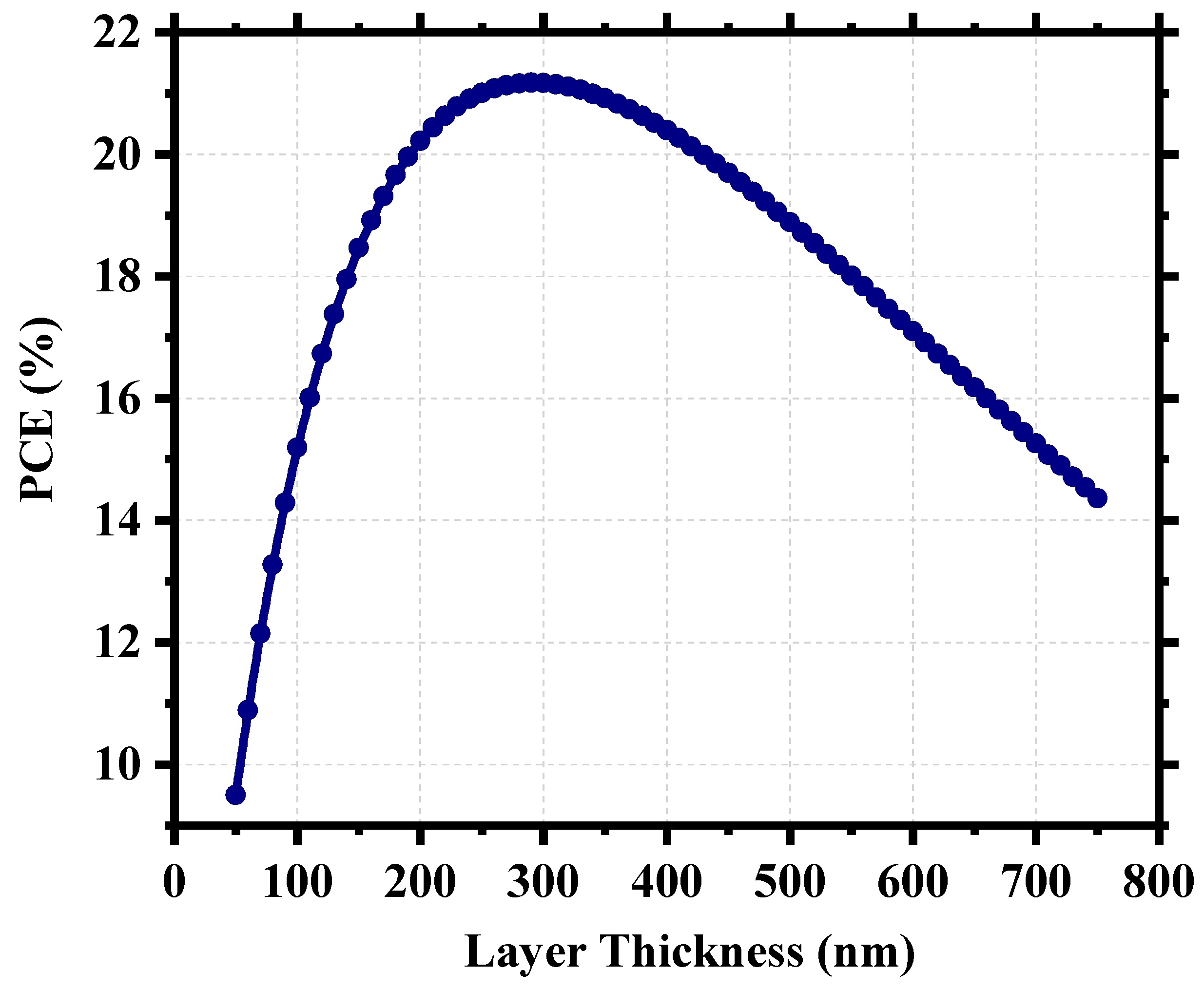
3.2. Optimization of Cs2TiI6 Perovskite Layer

For perovskite solar cells, the perovskite itself is the device’s active layer which absorbs photon energy and generates electron–hole pairs. That is why the physical properties of this layer are crucial to the overall device performance. Figure 7 shows our device’s power conversion efficiency (PCE) as a function of perovskite layer thickness and signifies the importance of having an optimized thickness. We have investigated the PCE of the device for a thickness range from 50 nm to 750 nm. For a very thin layer of perovskite, the photons with longer wavelengths face difficulties in being absorbed by the active layer [58] and, as the thickness increases, the effective bandgap withers, which aids the photon absorption [59]. In the case of a very thick layer, electrons and holes find a longer route to travel to reach the electrodes, which increases the probability of carrier recombination [52] and, as a result, the photocurrent decreases and we find a steep nature in the performance curve. The device possessed ~21% PCE when the perovskite thickness was around 300 nm, and the highest PCE was 21.18% for 290 nm. The already fabricated cell (Cs2TiBr6) of the same family had a thickness ~200 nm [27], and thus, we can choose a practically realizable thickness of 300 nm as the optimum thickness for this device with a PCE of 21.17%, Jsc of 32.93 mA/cm2, Voc of 0.79 V, and FF of 81.42%.

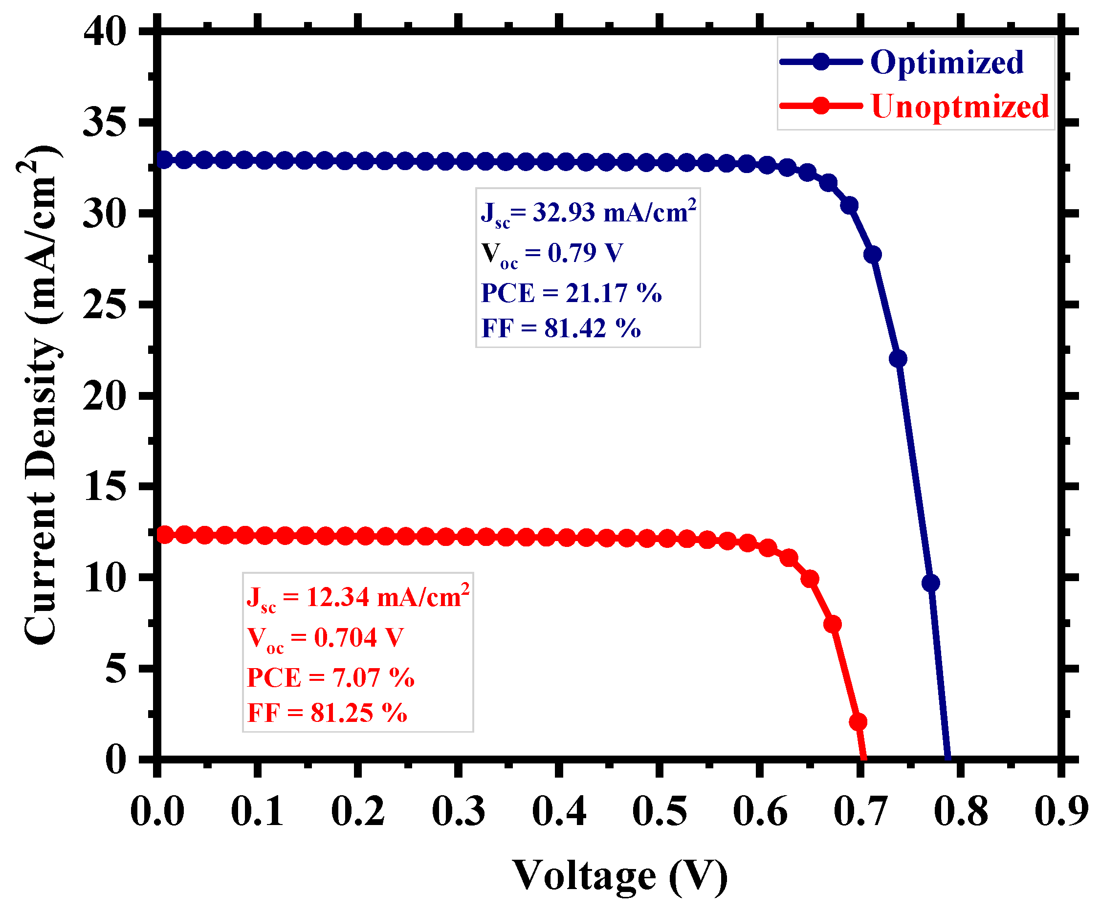
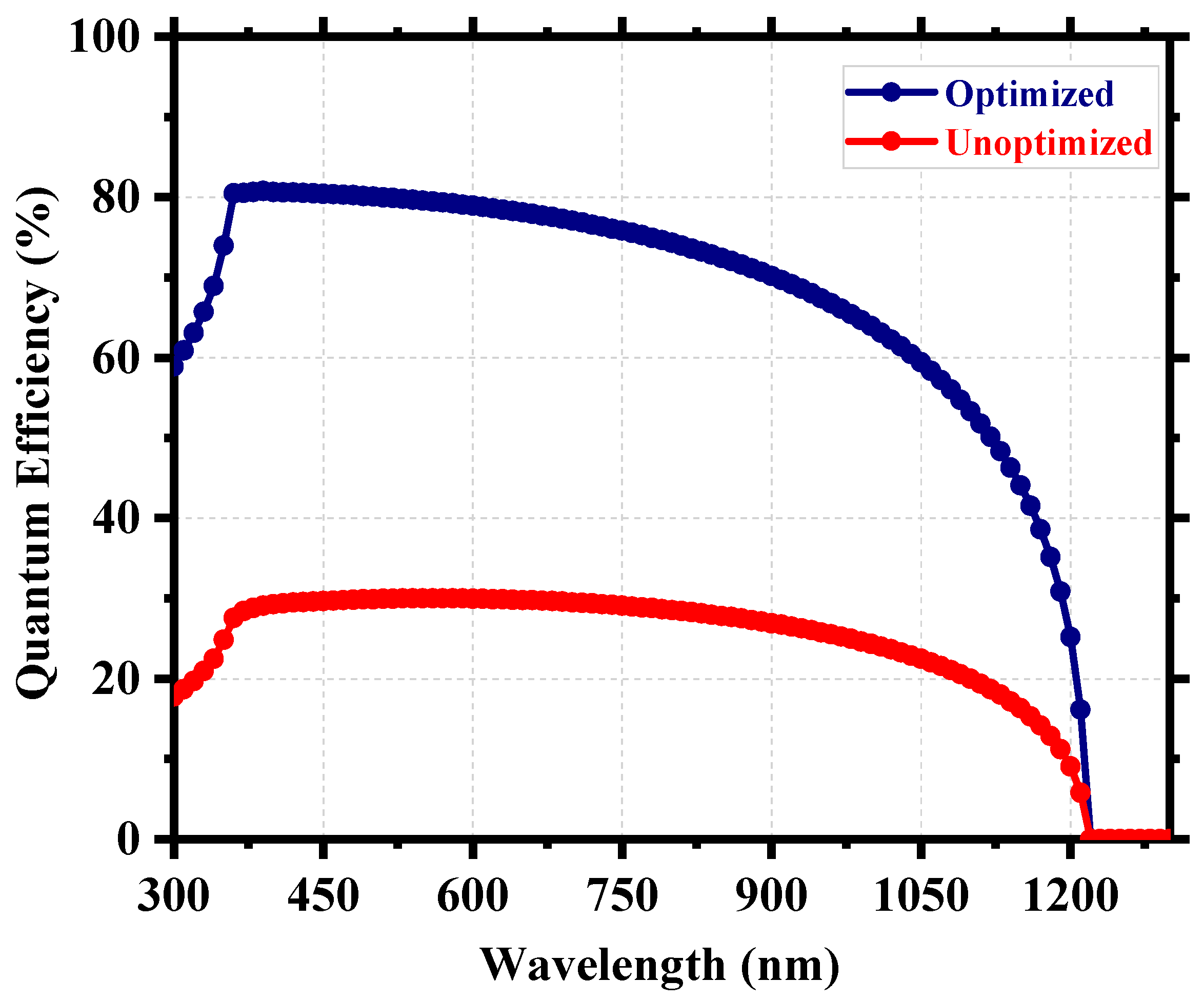
3.3. Optimum Solar Cell Performance

After the careful optimization of different device parameters, we achieved the optimum performance for a Cs2TiI6 perovskite solar cell (PSC). Figure 8 provides insight into the performance enhancement compared to the initially unoptimized state of the cell. A PCE of 21.17% with an implemented absorber defect density of 1014 cm−3 and a perovskite thickness of 300 nm was really promising. It suggests that the material processing and corresponding morphology of Cs2TiI6 thin film will be fundamentally crucial in achieving highly efficient Cs2TiI6 PSC. Figure 9 shows the quantum efficiency (QE) comparison, and Figure 10 provides the dark current comparison of the optimized final cell and the initially unoptimized cell. It can be seen that the solar cell possessed excellent QE with close to ~80% output around the visible spectrum. Also, owing to its narrow bandgap, the QE output of Cs2TiI6 existed for a wide range of wavelengths, supporting the calculation from Figure 1b, and it could have absorption cutoff up to ~1200 nm, and everything indicated that it could be a very good option as an active layer of the bottom cell in tandem solar cells. Table 2 provides a performance comparison with related numerical works on Cs2TiI6, and Table 3 shows a comparison with other PSCs from the Cs2TiIxBr6-x family. As Table 2 suggests, we achieved a competitive perovskite solar cell performance despite keeping defect density and perovskite thickness within a practically realizable range.
In contrast, the previous works on this material were carried out using very low defect densities and unrealistic carrier mobilities to achieve high performance, as discussed in detail in the introduction. We achieved excellent cell performance due to our meticulous approach regarding extracting device parameters from existing experimental data, careful choice of carrier transport layers to minimize band-offset, and optimization within a feasible range. Even with a practically feasible (relatively high) defect density and standard perovskite thickness, the performance can be competitive with proper optimization of all other essential design parameters. Also, it can be easily noticed from Table 3 that most of the works on the Cs2TiIxBr6-x family of perovskites are carried out using defect densities close to experimental values, and most of the absorbers’ thicknesses are around the range of ~200 nm to 400 nm with few below and above this range. Furthermore, based on the material processing, the carrier mobility might vary as well, and the possible impact of it is illustrated in Section S4 of the Supplementary Information. Figure S4 shows that the device’s PCE can vary within a range of ~19% to 24.5% for a change of one order of magnitude in carrier mobility. It is possible to enhance carrier mobility by producing high-quality thin films and, therefore, during material processing, much concentration is to be given to achieving high-quality films that might help yield even higher PCE.

4. Effects of Point Defects on Cell Performance

The material synthesis of Cs2TiI6 can give rise to different intrinsic point defects having defect formation energy within the material’s bandgap and acting as shallow or deep defect states. These point defects can cause performance degradation by acting as recombination centers for photogenerated charge carriers. Cs2TiI6 can have twelve possible point defects like vacancies (VCs, VTi, and VI), cation substitutions (CsTi, Tics), antisite substitutions (CsI, ICs, ITi, and TiI), and interstitials (Csi, Tii, and Ii) [26]. These point defects can act as single, double, or multilevel donors or acceptors and can be located within the material’s bandgap with high or low formation energies. Ju et al. [26] calculated the formation energies of these point defects for two different cases, i.e., I-lean/Ti-rich and I-rich/Ti-lean, and identified a standard chemical potential region to have thermodynamical stability of Cs2TiI6. Table S6 in Section S5 of the Supplementary Information provides these point defects’ charge transition levels and approximate locations. In terms of formation energy, they found that under two different conditions, there were differences in the formation energies of these point defects, and there were different point defects with the lowest formation energy in each case. Under I-rich/Ti-lean conditions, VI possessed the lowest energy and had a defect position (~0.57 eV) near the middle of the bandgap. This can be detrimental to the device’s performance by creating a deep defect state. Under I-lean/Ti-rich conditions, Tii possessed very low formation energy, most of its transition levels being within the mid-region of the bandgap (~0.35 eV, 0.45 eV, 0.73 eV, 0.92 eV), and can easily form a deep defect state and thus can cause some serious degradation to the device performance. There are other point defects like CsTi, which have higher formation energy in both conditions, and their defect position lies at the edge of the bandgap (~0.02 eV), and defects like these are likely to form shallow defect states and are less detrimental to the device.
Figure 11 shows an overview of the device PCE depending on the relative positions of the defects and the corresponding defect density within the perovskite. Figure S5 in the Supplementary Information shows the corresponding workflow for the calculation. We can find deep defect states within ~0.25–0.75 eV and quasi-shallow or shallow defect states around 0.0 eV (valence band maximum) and 1.02 eV (conduction band minimum). The device produced excellent PCE when the defect density was within the 1014 cm−3 mark or below, and the PCE started to decrease when the density increased towards 1015 cm−3. It still possessed a decent PCE of 11.47% around the deep defect region and 14.35% around the shallow defect region for Nt = 1015 cm−3. However, above 1015 cm−3, the degradation was drastic, and PCE reached as low as 2.15% around the deep defect region and 3.15% around the shallow defect region for Nt = 1016 cm−3. Therefore, it is rather easy to understand that the overall defect density within the perovskite is a crucial measure for the performance of Cs2TiI6-based PSCs, and anything above 1015 cm−3 will hamper the device performance significantly. The effect of deep and shallow defect states created by the point defects can be evaluated better from Figure 12. Here, we considered CsTi with transition level ɛ (0/1−) at 0.02 eV as the shallow defect state and VI with transition level ɛ (0/1+) at 0.57 eV as the deep defect state. Assuming I-lean/Ti-rich conditions are to be avoided in favor of the I-rich/Ti-lean conditions during the synthesis of Cs2TiI6 in order to suppress harmful Tii interstitial defects with very low formation energy, Figure 12 shows that, even under I-rich/Ti-lean conditions, there will be different impacts of shallow and deep defect states. With the increase in defect density, the impact becomes prominent as a higher number of VI defects will act as recombination centers causing a smaller number of electron–hole pairs to reach the electrodes and, in doing so, diminishing the device performance. For example, the device PCE gets reduced by almost 3% from a PCE of 14.35% to PCE of 11.47% at 1015 cm−3 defect density when there is a presence of a deep defect state of VI. Therefore, we can say that the device performance heavily relies on the defect density parameter within the active layer as well as the type of point defects formed within the layer. So, the defect engineering of Cs2TiI6 will be key for the success of Cs2TiI6 PSC technology.

5. Discussion

The computational results suggest that defect engineering will be crucial for the success of Cs2TiI6 PSC technology. Currently, the experimental reports on the synthesis and thin film formation of Cs2TiI6 are very limited. As the defect profile is closely related to the fabrication method and the derived morphology of the thin film, it calls for concentrated experimental investigation into different morphological features and techniques to produce higher-quality thin films to suppress the negative impacts of several defects. At present, techniques like melt-crystallization [26] and inverse temperature crystallization [60] have been utilized for producing Cs2TiI6 powder and thin film (~16 μm), respectively. However, for the thin film, Cs2TiI6 solution was unevenly distributed throughout the substrate and consisted of broken cube-shaped crystals instead of a bulk perovskite layer, a representative morphology for highly efficient perovskite solar cells [61]. Another study [62] tried to generate Cs2TiI6 nanocrystals from Cs2TiBr6 nanocrystals via a post-anion exchange reaction using the hot-injection method but could not succeed. Therefore, it is evident that Cs2TiI6 has a long way to go before it can truly live up to its full potential (as expected from the theoretical study) as a high-efficiency PSC material. One important step would be to realize a stable and uniform bulk Cs2TiI6 perovskite layer, and techniques like vapor deposition [27] and fast crystallization-deposition (FDC), also known as the anti-solvent method [61], can be explored to achieve that. Extensive engineering of the experimental parameters (e.g., reaction time and temperature of vapor deposition) could lead to high-quality thin film with reduced defect profile, and further engineering of different device parameters might pave the way for Cs2TiI6 PSC technology to reach its full potential for real world applications.

6. Conclusions

To conclude, we have numerically demonstrated the possibility of utilizing Cs2TiI6 as an active layer in perovskite solar cell (PSC) applications with competitive cell performance. At an unoptimized state, the cell exhibits a theoretical power conversion efficiency (PCE) of 7.07% with CuI and TiO2 as the carrier transport layers, which is substantially increased to 21.17% for an optimum absorber defect density of 1014 cm−3 and thickness of 300 nm. Our study further highlights the importance of material processing and choosing appropriate carrier transport layers for high-performance Cs2TiI6 PSC. We have computationally demonstrated that, even with a relatively high defect density and deep defect states due to several existing point defects in Cs2TiI6, it is still possible to reach a competitive cell performance via the proper optimization of essential design parameters, subject to further enhancement depending on the improvement in defect profiles by advanced thin film processing techniques. Also, the computed electronic and optical properties of Cs2TiI6 show its great potential as an alternative low-bandgap material for different solar cell applications.

Supplementary Materials

The following supporting information can be downloaded at: https://www.mdpi.com/article/10.3390/nano13142100/s1. It includes five sections. Section S1: SCAPS Simulation. Section S2: Validation of Numerical Setup. Section S3: Inorganic HTL Materials. Section S4: Carrier Mobility. Section S5: Point Defects. There are six supplementary tables. Supplementary Table S1: Material parameters used to validate the numerical setup. Supplementary Table S2: Defect parameters of different layers. Supplementary Table S3: Absorber/carrier transport layer interfacial defect parameters. Supplementary Table S4: Simulation parameters of different HTL materials. Supplementary Table S5: Performance comparison of different inorganic HTL materials. Supplementary Table S6: Point defects in Cs2TiI6 with charge transitions levels and approximate defect position within the bandgap. There are four supplementary figures. Supplementary Figure S1: Simulated J-V output with experimental comparison for FTO/TiO2/Cs2TiBr6/P3HT. Supplementary Figure S2: J-V output for different inorganic HTL materials. Supplementary Figure S3: Relative band alignment of different HTL materials with Cs2TiI6. Supplementary Figure S4: Possible performance variation based on carrier mobility. Figure S5: Workflow for calculating PCE as a function of defect position and defect density. References [26,27,50,51,52,53,54,63,64,65,66,67] are cited in the supplementary materials.

Author Contributions

Conceptualization, M.A.K.K.; Methodology, S.S.U.; Software, S.S.U., T.T.F. and D.A.; Validation, M.A.K.K. and V.P.; Investigation, S.S.U.; Writing—original draft, S.S.U. and M.A.K.K.; Writing—review & editing, M.A.K.K., V.P. and M.A.A.; Visualization, S.S.U., T.T.F. and D.A.; Supervision, V.P. and M.A.A.; Project administration, M.A.K.K.; Funding acquisition, V.P. All authors have read and agreed to the published version of the manuscript.

Funding

This research was funded by National Science Foundation under Grant No. 2230727.

Data Availability Statement

The data that support the findings of this study are available from the corresponding author upon reasonable request.

Acknowledgments

We acknowledge the computational facilities at the Center for Computational Research at the University at Buffalo, NY, USA (Accessed on 18 July 2023, http://hdl.handle.net/10477/79221). V.P. and D.A. gratefully acknowledge the support of the National Science Foundation under Grant No. 2230727. We acknowledge Marc Burgelman and his research team from the University of Gent, Belgium, for providing the SCAPS-1D simulation software.

Conflicts of Interest

The authors declare no conflict of interest.

References

  1. Jeon, N.J.; Noh, J.H.; Kim, Y.C.; Yang, W.S.; Ryu, S.; Seok, S.I. Solvent engineering for high-performance inorganic–organic hybrid perovskite solar cells. Nat. Mater. 2014, 13, 897–903. [Google Scholar] [CrossRef] [PubMed]
  2. Jeon, N.J.; Na, H.; Jung, E.H.; Yang, T.-Y.; Lee, Y.G.; Kim, G.; Shin, H.-W.; Seok, S.I.; Lee, J.; Seo, J. A fluorene-terminated hole-transporting material for highly efficient and stable perovskite solar cells. Nat. Energy 2018, 3, 682–689. [Google Scholar] [CrossRef]
  3. Kojima, A.; Teshima, K.; Shirai, Y.; Miyasaka, T. Organometal Halide Perovskites as Visible-Light Sensitizers for Photovoltaic Cells. J. Am. Chem. Soc. 2009, 131, 6050–6051. [Google Scholar] [CrossRef]
  4. Green, M.A.; Dunlop, E.D.; Hohl-Ebinger, J.; Yoshita, M.; Kopidakis, N.; Ho-Baillie, A.W. Solar cell efficiency tables (Version 55). Prog. Photovolt. Res. Appl. 2019, 28, 3–15. [Google Scholar] [CrossRef]
  5. Jeong, J.; Kim, M.; Seo, J.; Lu, H.; Ahlawat, P.; Mishra, A.; Yang, Y.; Hope, M.A.; Eickemeyer, F.T.; Kim, M.; et al. Pseudo-halide anion engineering for α-FAPbI3 perovskite solar cells. Nature 2021, 592, 381–385. [Google Scholar] [CrossRef]
  6. Yoshikawa, K.; Kawasaki, H.; Yoshida, W.; Irie, T.; Konishi, K.; Nakano, K.; Uto, T.; Adachi, D.; Kanematsu, M.; Uzu, H.; et al. Silicon heterojunction solar cell with interdigitated back contacts for a photoconversion efficiency over 26%. Nat. Energy 2017, 2, 17032. [Google Scholar] [CrossRef]
  7. Nie, W.; Blancon, J.-C.; Neukirch, A.J.; Appavoo, K.; Tsai, H.; Chhowalla, M.; Alam, M.A.; Sfeir, M.Y.; Katan, C.; Even, J.; et al. Light-activated photocurrent degradation and self-healing in perovskite solar cells. Nat. Commun. 2016, 7, 11574. [Google Scholar] [CrossRef] [PubMed] [Green Version]
  8. Adhikari, N.; Dubey, A.; Khatiwada, D.; Mitul, A.F.; Wang, Q.; Venkatesan, S.; Iefanova, A.; Zai, J.; Qian, X.; Kumar, M.; et al. Interfacial Study To Suppress Charge Carrier Recombination for High Efficiency Perovskite Solar Cells. ACS Appl. Mater. Interfaces 2015, 7, 26445–26454. [Google Scholar] [CrossRef] [PubMed]
  9. Xiao, Z.; Yuan, Y.; Shao, Y.; Wang, Q.; Dong, Q.; Bi, C.; Sharma, P.; Gruverman, A.; Huang, J. Giant switchable photovoltaic effect in organometal trihalide perovskite devices. Nat. Mater. 2014, 14, 193–198. [Google Scholar] [CrossRef]
  10. Snaith, H.J.; Abate, A.; Ball, J.M.; Eperon, G.E.; Leijtens, T.; Noel, N.K.; Stranks, S.D.; Wang, J.T.-W.; Wojciechowski, K.; Zhang, W. Anomalous Hysteresis in Perovskite Solar Cells. J. Phys. Chem. Lett. 2014, 5, 1511–1515. [Google Scholar] [CrossRef]
  11. Tang, S.; Deng, Y.; Zheng, X.; Bai, Y.; Fang, Y.; Dong, Q.; Wei, H.; Huang, J. Composition Engineering in Doctor-Blading of Perovskite Solar Cells. Adv. Energy Mater. 2017, 7, 1700302. [Google Scholar] [CrossRef]
  12. Giustino, F.; Snaith, H.J. Toward Lead-Free Perovskite Solar Cells. ACS Energy Lett. 2016, 1, 1233–1240. [Google Scholar] [CrossRef] [Green Version]
  13. Grätzel, M. The light and shade of perovskite solar cells. Nat. Mater. 2014, 13, 838–842. [Google Scholar] [CrossRef] [PubMed]
  14. Snaith, H.J. Present status and future prospects of perovskite photovoltaics. Nat. Mater. 2018, 17, 372–376. [Google Scholar] [CrossRef] [PubMed]
  15. Green, M.A.; Ho-Baillie, A.; Snaith, H.J. The emergence of perovskite solar cells. Nat. Photonics 2014, 8, 506–514. [Google Scholar] [CrossRef]
  16. Li, Z.; Yang, M.; Park, J.-S.; Wei, S.-H.; Berry, J.J.; Zhu, K. Stabilizing Perovskite Structures by Tuning Tolerance Factor: Formation of Formamidinium and Cesium Lead Iodide Solid-State Alloys. Chem. Mater. 2015, 28, 284–292. [Google Scholar] [CrossRef]
  17. Greul, E.; Petrus, M.L.; Binek, A.; Docampo, P.; Bein, T. Highly stable, phase pure Cs2AgBiBr6 double perovskite thin films for optoelectronic applications. J. Mater. Chem. A 2017, 5, 19972–19981. [Google Scholar] [CrossRef] [Green Version]
  18. Volonakis, G.; Haghighirad, A.A.; Milot, R.L.; Sio, W.H.; Filip, M.R.; Wenger, B.; Johnston, M.B.; Herz, L.M.; Snaith, H.J.; Giustino, F. Cs2InAgCl6: A New Lead-Free Halide Double Perovskite with Direct Band Gap. J. Phys. Chem. Lett. 2017, 8, 772–778. [Google Scholar] [CrossRef] [Green Version]
  19. Ju, M.-G.; Dai, J.; Ma, L.; Zeng, X.C. Lead-Free Mixed Tin and Germanium Perovskites for Photovoltaic Application. J. Am. Chem. Soc. 2017, 139, 8038–8043. [Google Scholar] [CrossRef]
  20. Gao, W.; Ran, C.; Xi, J.; Jiao, B.; Zhang, W.; Wu, M.; Hou, X.; Wu, Z. High-Quality Cs2 AgBiBr6 Double Perovskite Film for Lead-Free Inverted Planar Heterojunction Solar Cells with 2.2% Efficiency. ChemPhysChem 2018, 19, 1696–1700. [Google Scholar] [CrossRef]
  21. Chen, M.; Ju, M.-G.; Garces, H.F.; Carl, A.D.; Ono, L.K.; Hawash, Z.; Zhang, Y.; Shen, T.; Qi, Y.; Grimm, R.L.; et al. Highly stable and efficient all-inorganic lead-free perovskite solar cells with native-oxide passivation. Nat. Commun. 2019, 10, 16. [Google Scholar] [CrossRef] [PubMed] [Green Version]
  22. Ma, S.; Gu, X.; Kyaw, A.K.; Wang, D.H.; Priya, S.; Ye, T. Fully Inorganic CsSnI3-Based Solar Cells with >6% Efficiency and Enhanced Stability Enabled by Mixed Electron Transport Layer. ACS Appl. Mater. Interfaces 2020, 13, 1345–1352. [Google Scholar] [CrossRef] [PubMed]
  23. Ye, T.; Wang, K.; Hou, Y.; Yang, D.; Smith, N.; Magill, B.; Yoon, J.; Mudiyanselage, R.R.H.H.; Khodaparast, G.A.; Wang, K.; et al. Ambient-Air-Stable Lead-Free CsSnI3 Solar Cells with Greater than 7.5% Efficiency. J. Am. Chem. Soc. 2021, 143, 4319–4328. [Google Scholar] [CrossRef] [PubMed]
  24. Chung, I.; Song, J.-H.; Im, J.; Androulakis, J.; Malliakas, C.D.; Li, H.; Freeman, A.J.; Kenney, J.T.; Kanatzidis, M.G. CsSnI3: Semiconductor or Metal? High Electrical Conductivity and Strong Near-Infrared Photoluminescence from a Single Material. High Hole Mobility and Phase-Transitions. J. Am. Chem. Soc. 2012, 134, 8579–8587. [Google Scholar] [CrossRef]
  25. Wang, N.; Zhou, Y.; Ju, M.-G.; Garces, H.F.; Ding, T.; Pang, S.; Zeng, X.C.; Padture, N.P.; Sun, X.W. Heterojunction-Depleted Lead-Free Perovskite Solar Cells with Coarse-Grained B-γ-CsSnI3Thin Films. Adv. Energy Mater. 2016, 6, 1601130. [Google Scholar] [CrossRef]
  26. Ju, M.-G.; Chen, M.; Zhou, Y.; Garces, H.F.; Dai, J.; Ma, L.; Padture, N.P.; Zeng, X.C. Earth-Abundant Nontoxic Titanium(IV)-based Vacancy-Ordered Double Perovskite Halides with Tunable 1.0 to 1.8 eV Bandgaps for Photovoltaic Applications. ACS Energy Lett. 2018, 3, 297–304. [Google Scholar] [CrossRef]
  27. Chen, M.; Ju, M.-G.; Carl, A.D.; Zong, Y.; Grimm, R.L.; Gu, J.; Zeng, X.C.; Zhou, Y.; Padture, N.P. Cesium Titanium(IV) Bromide Thin Films Based Stable Lead-free Perovskite Solar Cells. Joule 2018, 2, 558–570. [Google Scholar] [CrossRef] [Green Version]
  28. Chakraborty, K.; Choudhury, M.G.; Paul, S. Numerical study of Cs2TiX6 (X = Br−, I−, F− and Cl−) based perovskite solar cell using SCAPS-1D device simulation. Sol. Energy 2019, 194, 886–892. [Google Scholar] [CrossRef]
  29. Samanta, M.; Ahmed, S.I.; Chattopadhyay, K.K.; Bose, C. Role of various transport layer and electrode materials in enhancing performance of stable environment-friendly Cs2TiBr6 solar cell. Optik 2020, 217, 164805. [Google Scholar] [CrossRef]
  30. Ahmed, S.; Jannat, F.; Khan, A.K.; Alim, M.A. Numerical development of eco-friendly Cs2TiBr6 based perovskite solar cell with all-inorganic charge transport materials via SCAPS-1D. Optik 2020, 225, 165765. [Google Scholar] [CrossRef]
  31. Jani, R.; Islam, T.; Al Amin, S.M.; Sami, S.U.; Shorowordi, K.M.; Hossain, M.I.; Chowdhury, S.; Nishat, S.S.; Ahmed, S. Exploring solar cell performance of inorganic Cs2TiBr6 halide double perovskite: A numerical study. Superlattices Microstruct. 2020, 146, 106652. [Google Scholar] [CrossRef]
  32. Moiz, S.A.; Alahmadi, A.N.M. Design of Dopant and Lead-Free Novel Perovskite Solar Cell for 16.85% Efficiency. Polymers 2021, 13, 2110. [Google Scholar] [CrossRef]
  33. Moiz, S.A.; Alahmadi, A.N.M.; Aljohani, A.J. Design of a Novel Lead-Free Perovskite Solar Cell for 17.83% Efficiency. IEEE Access 2021, 9, 54254–54263. [Google Scholar] [CrossRef]
  34. Moiz, S.A. Optimization of Hole and Electron Transport Layer for Highly Efficient Lead-Free Cs2TiBr6-Based Perovskite Solar Cell. Photonics 2022, 9, 23. [Google Scholar] [CrossRef]
  35. Khan, A.K.; Urmi, S.S.; Ferdous, T.T.; Azam, S.; Alim, M.A. Highly efficient Cesium Titanium (IV) Bromide perovskite solar cell and its point defect investigation: A computational study. Superlattices Microstruct. 2021, 156, 106946. [Google Scholar] [CrossRef]
  36. Shivesh, K.; Alam, I.; Kushwaha, A.K.; Kumar, M.; Singh, S.V. Investigating the theoretical performance ofCs2TiBr6-based perovskite solar cell with La-dopedBaSnO3andCuSbS2as the charge transport layers. Int. J. Energy Res. 2021, 46, 6045–6064. [Google Scholar] [CrossRef]
  37. Ahmad, O.; Rashid, A.; Ahmed, M.W.; Nasir, M.F.; Qasim, I. Performance evaluation of Au/p-CdTe/Cs2TiI6/n-TiO2/ITO solar cell using SCAPS-1D. Opt. Mater. 2021, 117, 111105. [Google Scholar] [CrossRef]
  38. Chakraborty, K.; Choudhury, M.G.; Paul, S. Study of Physical, Optical, and Electrical Properties of Cesium Titanium (IV)-Based Single Halide Perovskite Solar Cell. IEEE J. Photovolt. 2021, 11, 386–390. [Google Scholar] [CrossRef]
  39. Zhao, P.; Su, J.; Guo, Y.; Wang, L.; Lin, Z.; Hao, Y.; Ouyang, X.; Chang, J. Cs2TiI6: A potential lead-free all-inorganic perovskite material for ultrahigh-performance photovoltaic cells and alpha-particle detection. Nano Res. 2021, 15, 2697–2705. [Google Scholar] [CrossRef]
  40. Zhang, T.; He, Q.; Yu, J.; Chen, A.; Zhang, Z.; Pan, J. Recent progress in improving strategies of inorganic electron transport layers for perovskite solar cells. Nano Energy 2022, 104, 107918. [Google Scholar] [CrossRef]
  41. Kranthiraja, K.; Parashar, M.; Mehta, R.K.; Aryal, S.; Temsal, M.; Kaul, A.B. Stability and degradation in triple cation and methyl ammonium lead iodide perovskite solar cells mediated via Au and Ag electrodes. Sci. Rep. 2022, 12, 18574. [Google Scholar] [CrossRef] [PubMed]
  42. Giannozzi, P.; Baroni, S.; Bonini, N.; Calandra, M.; Car, R.; Cavazzoni, C.; Ceresoli, D.; Chiarotti, G.L.; Cococcioni, M.; Dabo, I. QUANTUM ESPRESSO: A modular and open-source software project for quantum simulations of materials. J. Phys. Condens. Matter. 2009, 21, 395502. [Google Scholar] [CrossRef] [PubMed]
  43. Giannozzi, P.; Andreussi, O.; Brumme, T.; Bunau, O.; Nardelli, M.B.; Calandra, M.; Car, R.; Cavazzoni, C.; Ceresoli, D.; Cococcioni, M. Advanced capabilities for materials modelling with Quantum ESPRESSO. J. Phys. Condens. Matter. 2017, 29, 465901. [Google Scholar] [CrossRef] [PubMed] [Green Version]
  44. Smart, T.J.; Wu, F.; Govoni, M.; Ping, Y. Fundamental principles for calculating charged defect ionization energies in ultrathin two-dimensional materials. Phys. Rev. Mater. 2018, 2, 124002. [Google Scholar] [CrossRef]
  45. Mosey, N.J.; Carter, E.A. Ab initio evaluation of Coulomb and exchange parameters for DFT+ U calculations. Phys. Rev. B 2007, 76, 155123. [Google Scholar] [CrossRef]
  46. Grosso, G.; Parravicini, G.P. Solid State Physics; Academic Press: Cambridge, MA, USA, 2013. [Google Scholar]
  47. Burgelman, M.; Nollet, P.; Degrave, S. Modelling polycrystalline semiconductor solar cells. Thin Solid Films 2000, 361–362, 527–532. [Google Scholar] [CrossRef]
  48. Verschraegen, J.; Burgelman, M. Numerical modeling of intra-band tunneling for heterojunction solar cells in scaps. Thin Solid Films 2007, 515, 6276–6279. [Google Scholar] [CrossRef]
  49. Decock, K.; Khelifi, S.; Burgelman, M. Modelling multivalent defects in thin film solar cells. Thin Solid Films 2011, 519, 7481–7484. [Google Scholar] [CrossRef]
  50. Noh, M.F.M.; Teh, C.H.; Daik, R.; Lim, E.L.; Yap, C.C.; Ibrahim, M.A.; Ludin, N.A.; Yusoff, A.R.B.M.; Jang, J.; Teridi, M.A.M. The architecture of the electron transport layer for a perovskite solar cell. J. Mater. Chem. C 2017, 6, 682–712. [Google Scholar] [CrossRef]
  51. Lakhdar, N.; Hima, A. Electron transport material effect on performance of perovskite solar cells based on CH3NH3GeI3. Opt. Mater. 2019, 99, 109517. [Google Scholar] [CrossRef]
  52. Yang, C.; Kneiß, M.; Schein, F.-L.; Lorenz, M.; Grundmann, M. Room-temperature Domain-epitaxy of Copper Iodide Thin Films for Transparent CuI/ZnO Heterojunctions with High Rectification Ratios Larger than 109. Sci. Rep. 2016, 6, 21937. [Google Scholar] [CrossRef] [PubMed] [Green Version]
  53. Kanoun, A.-A.; Kanoun, M.B.; Merad, A.E.; Goumri-Said, S. Toward development of high-performance perovskite solar cells based on CH3NH3GeI3 using computational approach. Sol. Energy 2019, 182, 237–244. [Google Scholar] [CrossRef]
  54. Helander, M.G.; Greiner, M.T.; Wang, Z.B.; Tang, W.M.; Lu, Z.H. Work function of fluorine doped tin oxide. J. Vac. Sci. Technol. A 2011, 29, 011019. [Google Scholar] [CrossRef]
  55. Karimi, E.; Ghorashi, S. Investigation of the influence of different hole-transporting materials on the performance of perovskite solar cells. Optik 2017, 130, 650–658. [Google Scholar] [CrossRef]
  56. Abdelaziz, W.; Shaker, A.; Abouelatta, M.; Zekry, A. Possible efficiency boosting of non-fullerene acceptor solar cell using device simulation. Opt. Mater. 2019, 91, 239–245. [Google Scholar] [CrossRef]
  57. Salah, M.M.; Abouelatta, M.; Shaker, A.; Hassan, K.M.; Saeed, A. A comprehensive simulation study of hybrid halide perovskite solar cell with copper oxide as HTM. Semicond. Sci. Technol. 2019, 34, 115009. [Google Scholar] [CrossRef]
  58. Liu, D.; Gangishetty, M.K.; Kelly, T.L. Effect of CH3NH3PbI3 thickness on device efficiency in planar heterojunction perovskite solar cells. J. Mater. Chem. A 2014, 2, 19873–19881. [Google Scholar] [CrossRef] [Green Version]
  59. Alharbi, S.; Darwish, A.; Al Garni, S.; ElSaeedy, H.; El-Rahman, K.A. Influence of thickness and annealing on linear and nonlinear optical properties of manganese (III) chloride tetraphenyl porphine (MnTPPCl) organic thin films. Infrared Phys. Technol. 2016, 78, 77–83. [Google Scholar] [CrossRef]
  60. Aslam, S.; Bakhsh, S.; Yusof, Y.; Rahman, M.Y.A.; Ibrahim, A.R.; Samsuri, S.A.M. Structural and optical properties of vacancy-ordered double halide perovskites, Cs2TiI6 films. Mater. Sci. Eng. B 2023, 296, 116645. [Google Scholar] [CrossRef]
  61. Kim, H.-S.; Hagfeldt, A.; Park, N.-G. Morphological and compositional progress in halide perovskite solar cells. Chem. Commun. 2018, 55, 1192–1200. [Google Scholar] [CrossRef]
  62. Grandhi, G.K.; Matuhina, A.; Liu, M.; Annurakshita, S.; Ali-Löytty, H.; Bautista, G.; Vivo, P. Lead-Free Cesium Titanium Bromide Double Perovskite Nanocrystals. Nanomaterials 2021, 11, 1458. [Google Scholar] [CrossRef] [PubMed]
  63. Bendib, T.; Bencherif, H.; Abdi, M.; Meddour, F.; Dehimi, L.; Chahdi, M. Combined optical-electrical modeling of perovskite solar cell with an optimized design. Opt. Mater. 2020, 109, 110259. [Google Scholar] [CrossRef]
  64. Du, H.-J.; Wang, W.-C.; Zhu, J.-Z. Device simulation of lead-free CH3 NH3 SnI3 perovskite solar cells with high efficiency. Chin. Phys. B 2016, 25, 108802. [Google Scholar] [CrossRef]
  65. Azri, F.; Meftah, A.; Sengouga, N.; Meftah, A. Electron and hole transport layers optimization by numerical simulation of a perovskite solar cell. Sol. Energy 2019, 181, 372–378. [Google Scholar] [CrossRef]
  66. Hossain, M.I.; Alharbi, F.H.; Tabet, N. Copper oxide as inorganic hole transport material for lead halide perovskite based solar cells. Sol. Energy 2015, 120, 370–380. [Google Scholar] [CrossRef]
  67. Li, W.; Li, W.; Feng, Y.; Yang, C. Numerical analysis of the back interface for high efficiency wide band gap chalcopyrite solar cells. Sol. Energy 2019, 180, 207–215. [Google Scholar] [CrossRef]
Figure 1. DFT calculation of Cs2TiI6: (a) Graphical representation of crystal structure, (b) computed optical absorption coefficient of Cs2TiI6 and Si, (c) band structure of Cs2TiI6 and (d) projected density of states (DOS) and total DOS of Cs2TiI6.
Nanomaterials 13 02100 g001
Figure 2. Cs2TiI6-based perovskite solar cell: (a) constituent layers and (b) corresponding energy levels.
Nanomaterials 13 02100 g002
Figure 3. Simulated current density vs. voltage (J-V) output of the cell.
Nanomaterials 13 02100 g003
Figure 4. Simulated quantum efficiency (QE) as a function of wavelength for the cell.
Nanomaterials 13 02100 g004
Figure 5. J-V output for different interfacial defect densities.
Nanomaterials 13 02100 g005
Figure 6. J-V output for different absorber defect densities.
Nanomaterials 13 02100 g006
Figure 7. Power conversion efficiency (PCE) as a function of perovskite thickness.
Nanomaterials 13 02100 g007
Figure 8. Comparison of the optimized and unoptimized cell.
Nanomaterials 13 02100 g008
Figure 9. QE comparison of the optimized and unoptimized cell.
Nanomaterials 13 02100 g009
Figure 10. Dark current comparison of the optimized and unoptimized cell.
Nanomaterials 13 02100 g010
Figure 11. PCE as a function of defect position and defect density.
Nanomaterials 13 02100 g011
Figure 12. Device PCE as a function of defect density for shallow and deep defects.
Nanomaterials 13 02100 g012
Table 1. Related material parameters and their corresponding values.
ParameterCs2TiI6n-TiO2p-CuIFTO
Layer thickness, d (nm)2005050150
Bandgap, Eg (eV)1.023.23.13.5
Electron affinity, χ (eV)4.04.12.14.4
Relative permittivity, εr5.3696.59
Conduction band density of states, Nc (cm−3)4.96 × 10191 × 10212.8 × 10192.2 × 1018
Valence band density of states, Nv (cm−3)1.75 × 10192 × 10201 × 10191.8 × 1019
Electron mobility, μn (cm2/V s)0.2362010020
Hole mobility, μp (cm2/V s)0.1711043.910
Donor concentration, ND (cm−3)3 × 10191 × 101901 × 1019
Acceptor concentration, NA (cm−3)3 × 101803 × 10180
Thermal velocity of electron, Vth(n) (cm/s)1 × 1071 × 1071 × 1071 × 107
Thermal velocity of hole, Vth(h) (cm/s)1 × 1071 × 1071 × 1071 × 107
Reference[26,27][27,51][52,53][54,55]
Table 2. Overall comparison of related numerical reports on Cs2TiI6 PSCs.
Cell StructureAbsorber
Defect
Density (cm−3)
Absorber Thickness (nm)PCE (%)Jsc (mA/cm2)Voc (V)FF (%)
CuSCN/Cs2TiI6/CdS/Si [28]-15003.134.6--
ITO/TiO2/Cs2TiI6/CdTe/Au [37]-783015.0625.081.3943.17
FTO/TiO2/Cs2TiI6/CuSCN/Ag [38]1010100016.3122.741.7441
FTO/PEDOT: PSS/Cs2TiI6/C60/Ag [39]10105022.7039.50.68583.7
FTO/TiO2/Cs2TiI6/CuI/Au [This Work]101430021.1732.930.7981.42
Table 3. Comparison with some other numerical reports on Cs2TiIxBr6-x family of PSCs.
Cell StructureAbsorber Defect
Density (cm−3)
Absorber Thickness (nm)PCE (%)Jsc (mA/cm2)Voc (V)FF (%)
CuSCN/Cs2TiBr6/CdS/Si [28]-10006.688.9--
FTO/TiO2/Cs2TiBr6/NiO/Au [29]-3008.5110.251.1273.59
FTO/SnO2/Cs2TiBr6/MoO3/Au [30]101413011.498.661.5386.45
FTO/TiO2/Cs2TiBr6/Cu2O/Au [31]101580014.6825.821.1051.74
ITO/NPB/Cs2TiBr6/PCBM/BCP/Ag [32]101735016.8516.661.2978.10
AZO/TiO2/Cs2TiBr6/PEDOT:PSS/Au [33]-20017.8318.201.3871.00
CeOx/Cs2TiBr6/NPB [34]101520017.9415.371.3387.00
FTO/ZnO/Cs2TiBr6/MoO3/Au [35]101440018.1513.601.5387.23
FTO/BaSnO3/Cs2TiBr6/CuSbS2/Au [36]1013100029.1329.601.1188.58
FTO/TiO2/Cs2TiI6/CuI/Au [This Work]101430021.1732.930.7981.42
Disclaimer/Publisher’s Note: The statements, opinions and data contained in all publications are solely those of the individual author(s) and contributor(s) and not of MDPI and/or the editor(s). MDPI and/or the editor(s) disclaim responsibility for any injury to people or property resulting from any ideas, methods, instructions or products referred to in the content.

