Nanostructured Thermoelectric Films Synthesised by Spark Ablation and Their Oxidation Behaviour

 , ,
, ,  and
and
Abstract
1. Introduction
2. Experimental
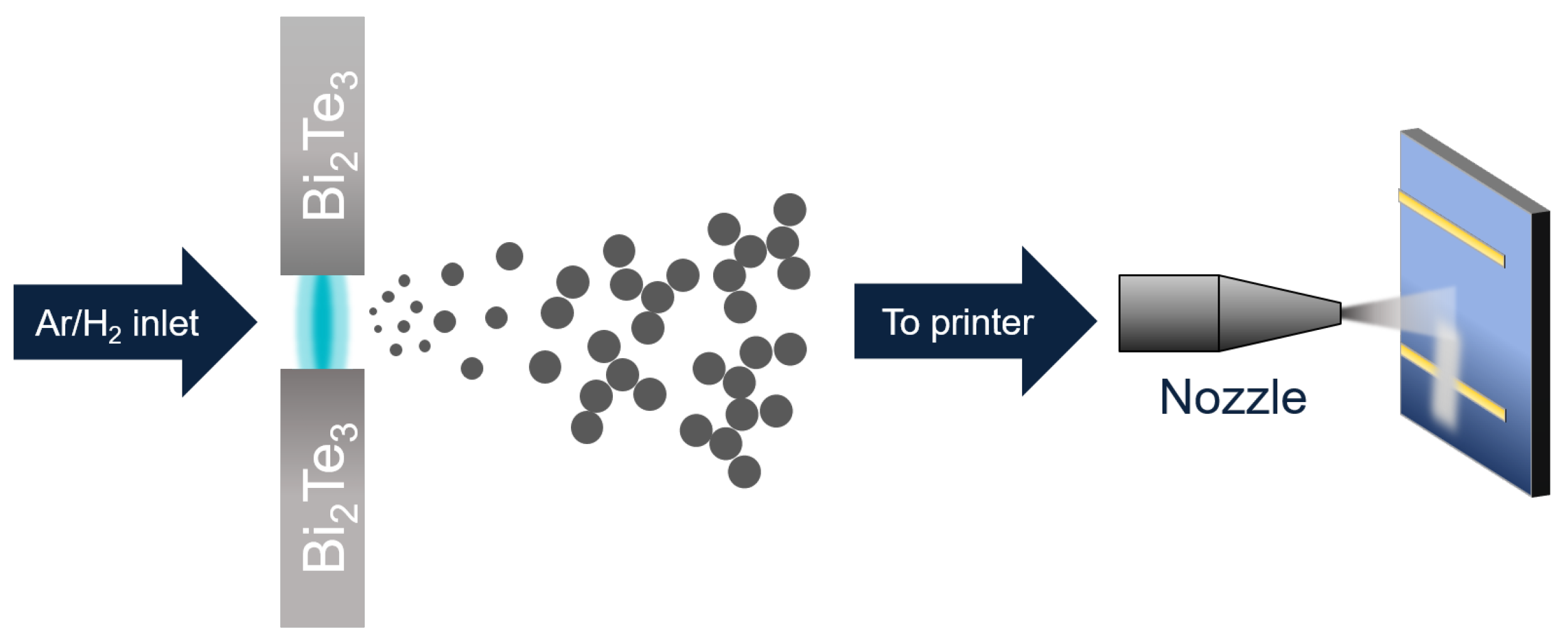
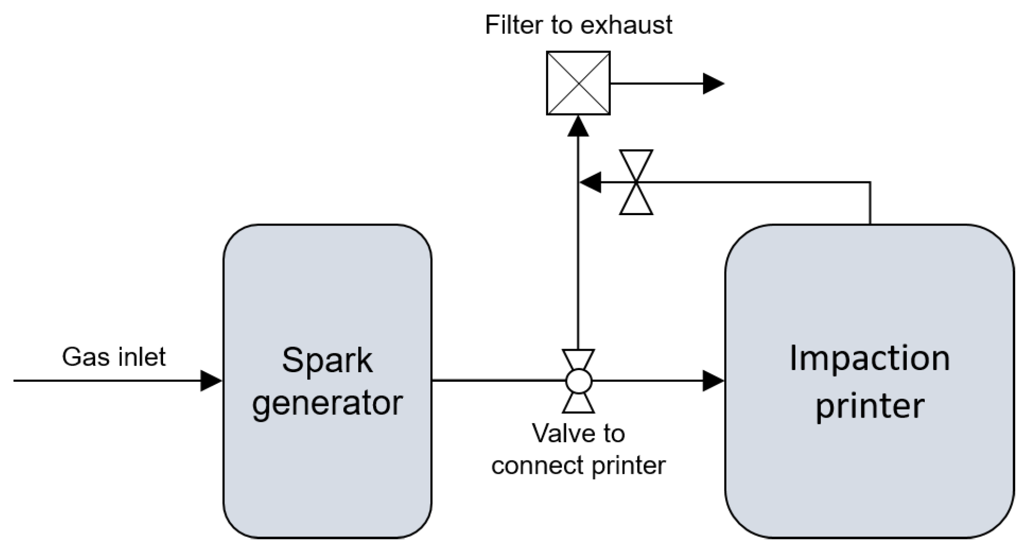
2.1. Nanoparticle Generation and Deposition
2.2. Structure Characterisation
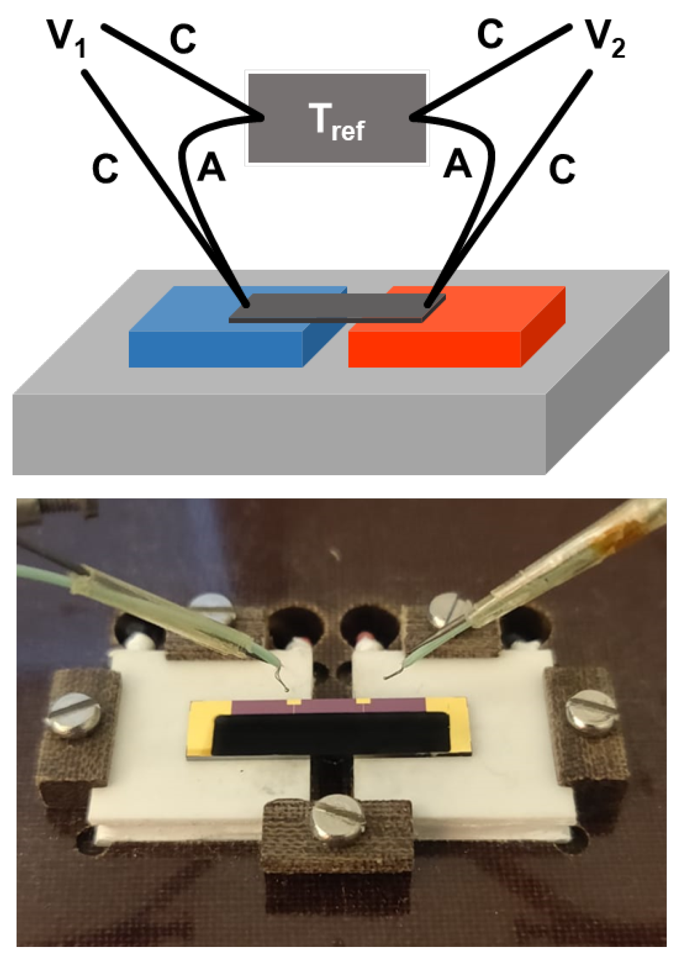
2.3. Thermoelectric Characterisation
3. Results and Discussion
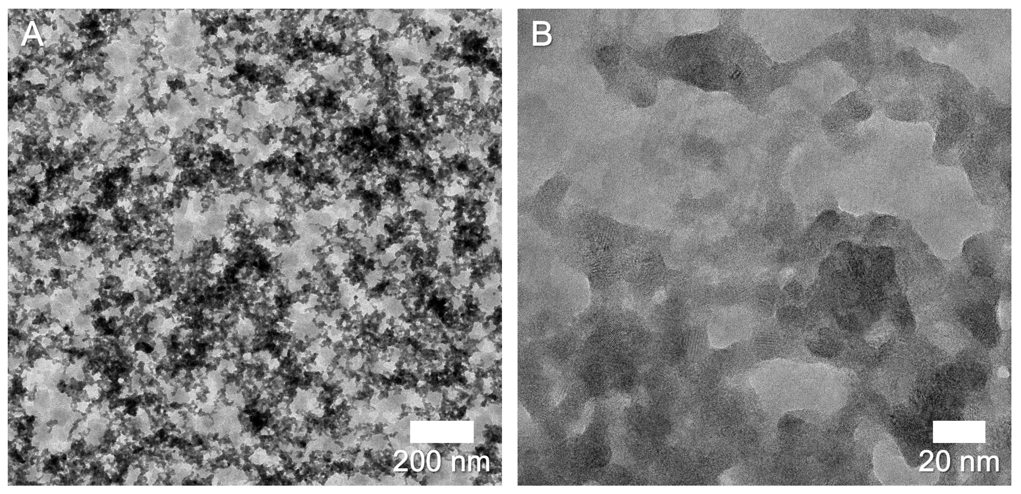
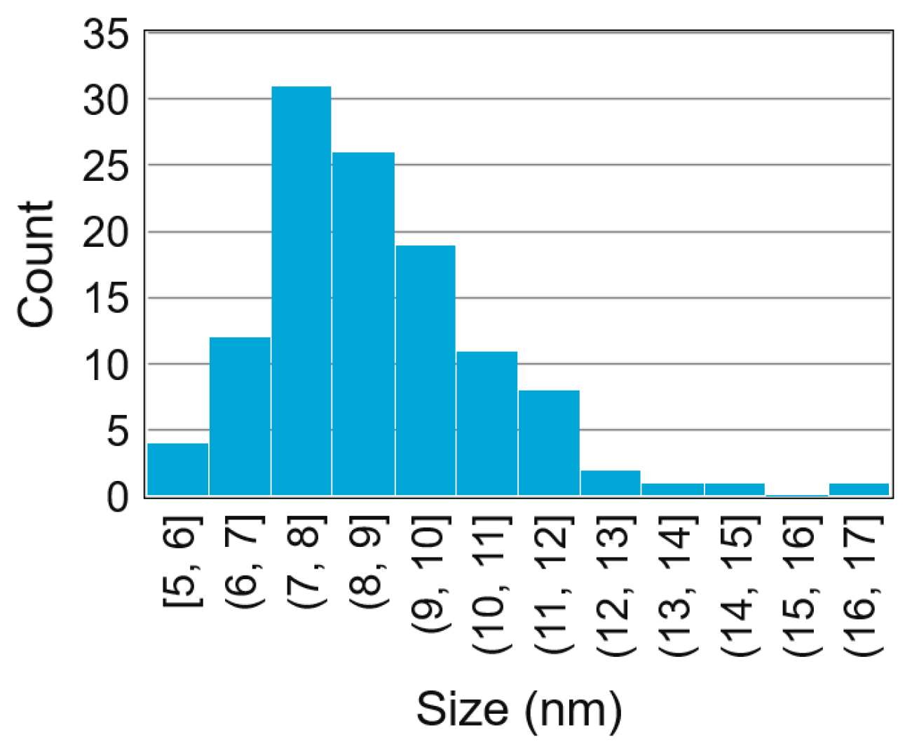
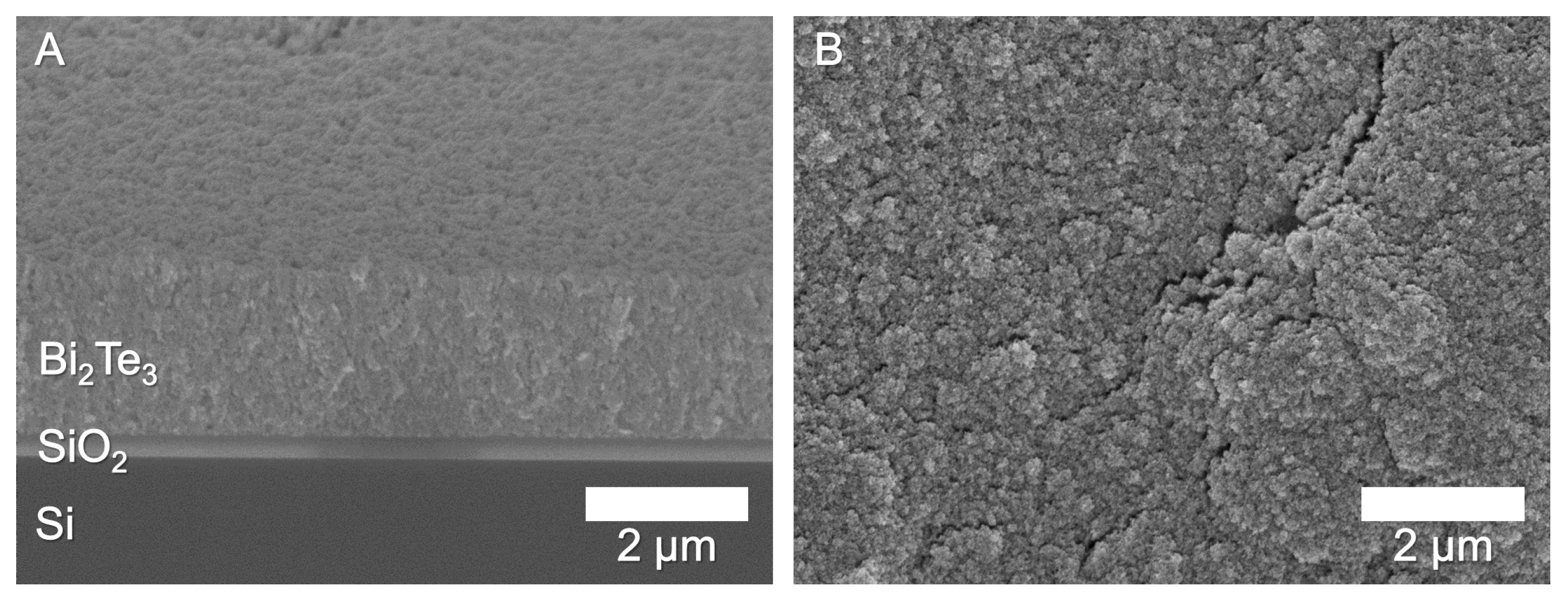
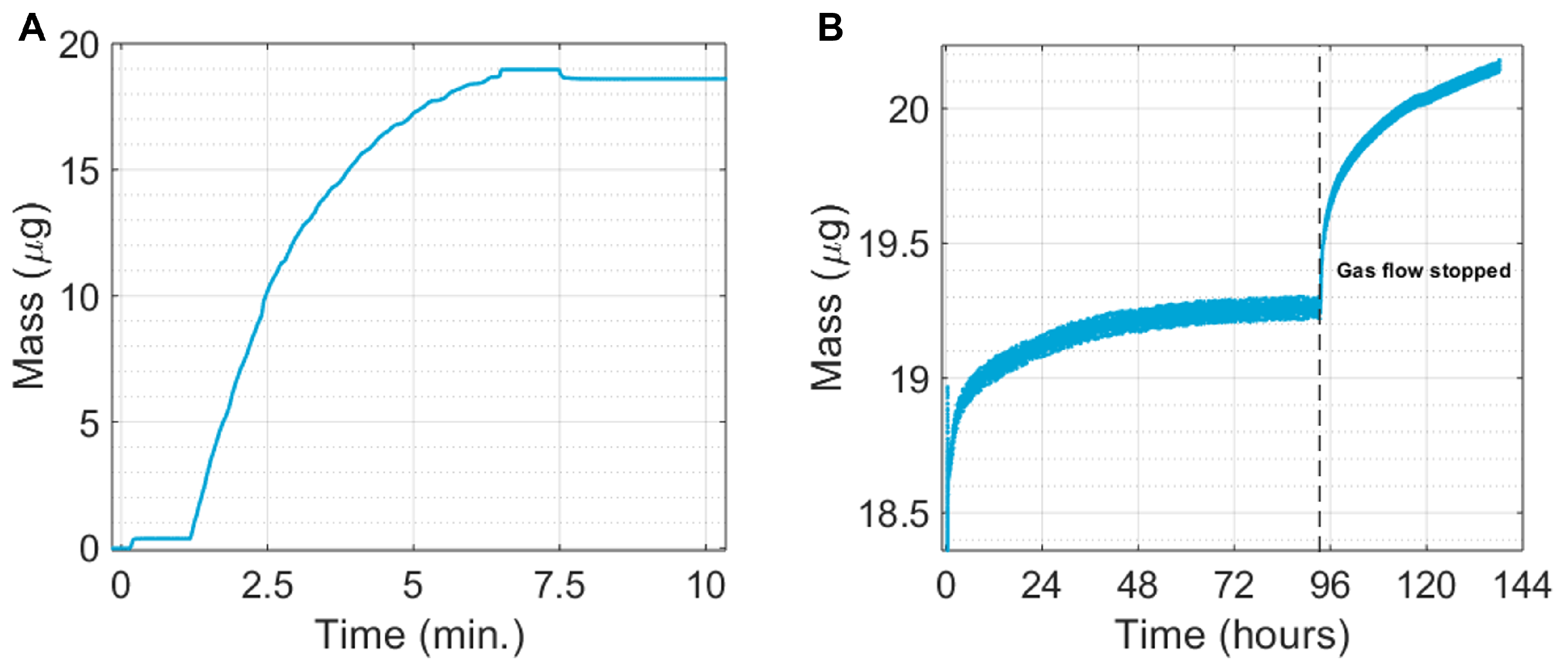
3.1. Nanostructure and Composition
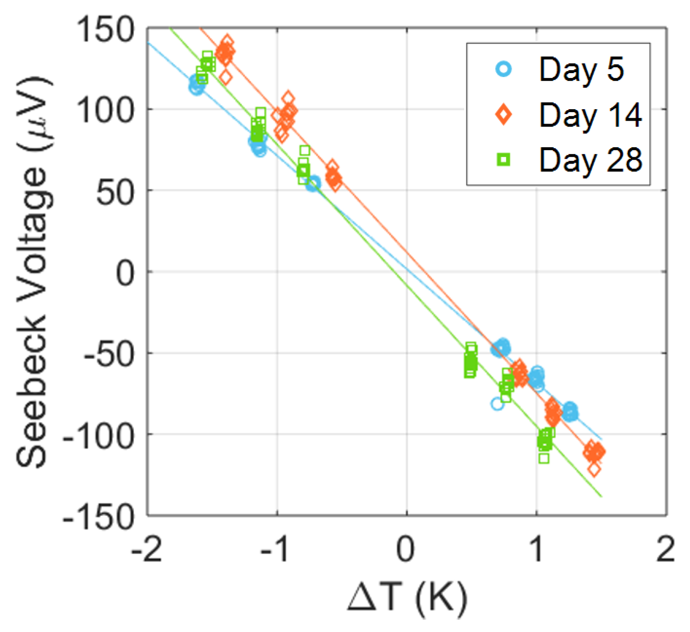
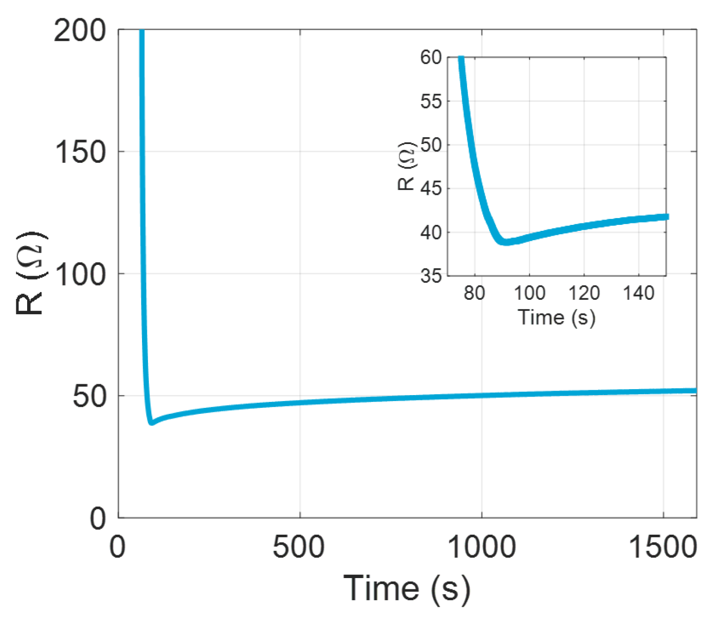
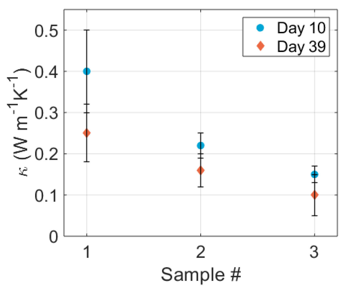
3.2. Thermoelectric Performance
4. Discussion
5. Conclusions
Author Contributions
Funding
Data Availability Statement
Acknowledgments
Conflicts of Interest
Abbreviations
| TE | Thermoelectric |
| LED | Light emitting diode |
| TEG | Thermoelectric generator |
| IC | Integrated circuit |
| MEMS | Microelectromechanical system |
| NASA | National Aeronautics and Space Administration |
| TEM | Transmission electron microscopy |
| FoM | Figure of merit |
| PGEC | Phonon glass, electron crystal |
| XRD | X-ray diffraction |
| SEM | Scanning electron microscopy |
| QCM | Quartz crystal microbalance |
| PCB | Printed circuit board |
| TDTR | Time domain thermoreflectance |
Appendix A
Appendix A.1

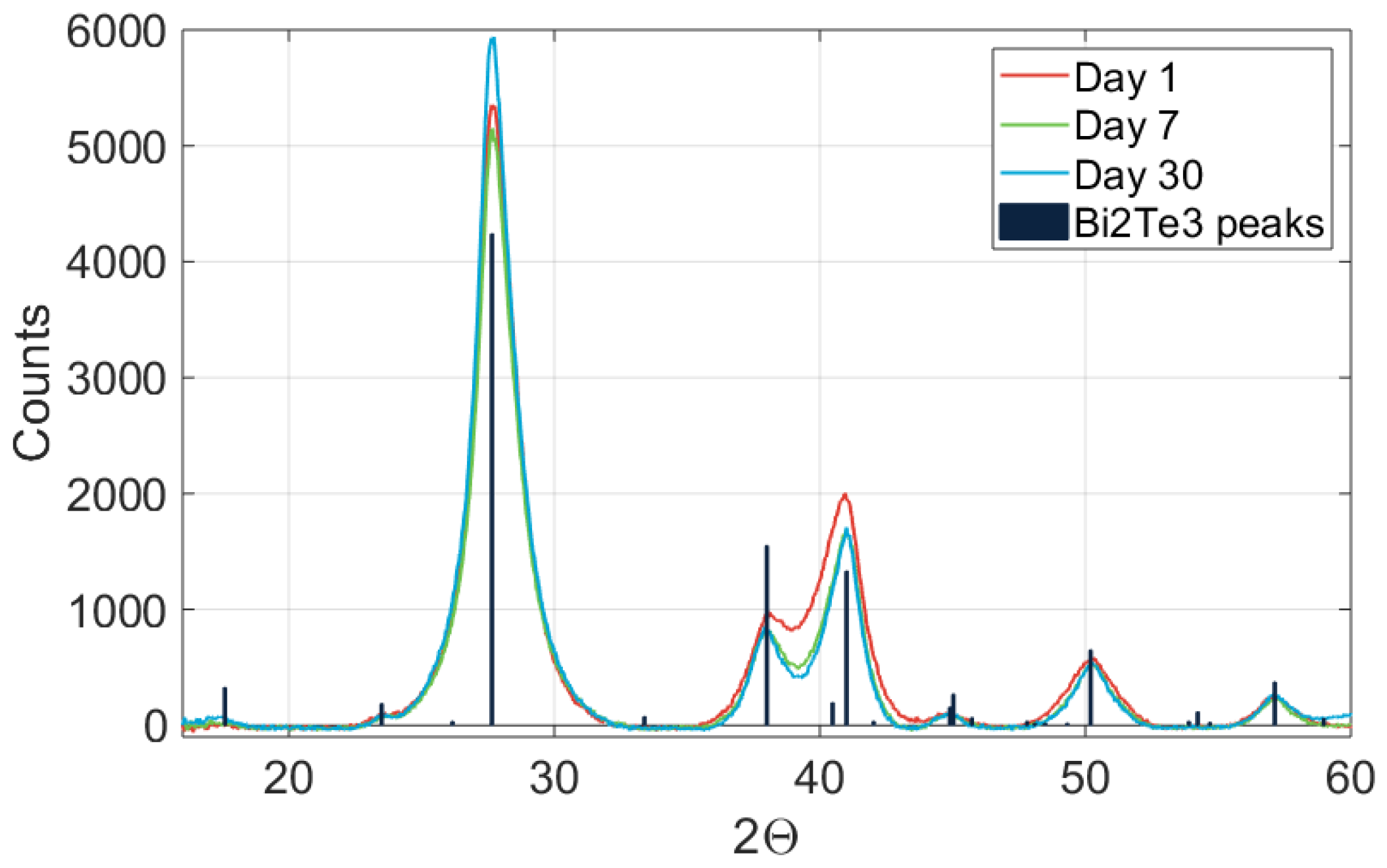
| Day | (rad) | (rad) | (nm) |
|---|---|---|---|
| Day 1 | 0.4824 | 0.0304 | 5.1 |
| Day 7 | 0.4824 | 0.0291 | 5.3 |
| Day 30 | 0.4838 | 0.0281 | 5.5 |
References
- Lee, W.; Lee, J. Development of a compact thermoelectric generator consisting of printed circuit heat exchangers. Energy Convers. Manag. 2018, 171, 1302–1310. [Google Scholar]
- He, J.; Tritt, T.M. Advances in thermoelectric materials research: Looking back and moving forward. Science 2017, 357. [Google Scholar] [CrossRef] [PubMed]
- Minnich, A.J.; Dresselhaus, M.S.; Ren, Z.F.; Chen, G. Bulk nanostructured thermoelectric materials: Current research and future prospects. Energy Environ. Sci. 2009, 2, 466–479. [Google Scholar]
- Yang, L.; Chen, Z.G.; Dargusch, M.S.; Zou, J. High Performance Thermoelectric Materials: Progress and Their Applications. Adv. Energy Mater. 2018, 8, 1701797. [Google Scholar] [CrossRef]
- Rowe, D. (Ed.) Thermoelectrics Handbook; CRC Press: Boca Raton, FL, USA, 2018. [Google Scholar]
- Yan, J.; Liao, X.; Yan, D.; Chen, Y. Review of Micro Thermoelectric Generator. J. Microelectromechanical Syst. 2018, 27, 1–18. [Google Scholar] [CrossRef]
- Yin, Y.; Tudu, B.; Tiwari, A. Recent advances in oxide thermoelectric materials and modules. Vacuum 2017, 146, 356–374. [Google Scholar] [CrossRef]
- Witting, I.T.; Chasapis, T.C.; Ricci, F.; Peters, M.; Heinz, N.A.; Hautier, G.; Snyder, G.J. The Thermoelectric Properties of Bismuth Telluride. Adv. Electron. Mater. 2019, 5, 1800904. [Google Scholar] [CrossRef]
- Feng, Y.; Jiang, X.; Ghafari, E.; Kucukgok, B.; Zhang, C.; Ferguson, I.; Lu, N. Metal oxides for thermoelectric power generation and beyond. Adv. Compos. Hybrid Mater. 2018, 1, 114–126. [Google Scholar] [CrossRef]
- Liu, W.; Jie, Q.; Kim, H.S.; Ren, Z. Current progress and future challenges in thermoelectric power generation: From materials to devices. Acta Mater. 2015, 87, 357–376. [Google Scholar] [CrossRef]
- Ouyang, Y.; Zhang, Z.; Li, D.; Chen, J.; Zhang, G. Emerging Theory, Materials, and Screening Methods: New Opportunities for Promoting Thermoelectric Performance. Annalen Der Physik 2019, 1800437. [Google Scholar] [CrossRef]
- Tritt, T.M. Thermoelectric Phenomena, Materials, and Applications. Annu. Rev. Mater. Res. 2011, 41, 433–448. [Google Scholar] [CrossRef]
- Matthes, C.S.R.; Woerner, D.F.; Hendricks, T.J.; Fleurial, J.; Oxnevad, K.I.; Barklay, C.D.; Zakrajsek, J.F. Next-generation radioisotope thermoelectric generator study. In Proceedings of the 2018 IEEE Aerospace Conference, Big Sky, MT, USA, 3–10 March 2018; pp. 1–9. [Google Scholar]
- Bottner, H.; Nurnus, J.; Schubert, A.; Volkert, F. New high density micro structured thermogenerators for stand alone sensor systems. In Proceedings of the 2007 26th International Conference on Thermoelectrics, Jeju, Republic of Korea, 3–5 June 2007; pp. 306–309. [Google Scholar]
- Waldrop, S.; Morelli, D. Low-Temperature Thermoelectric Properties of PtSb2 for Cryogenic Peltier Cooling Applications. J. Electron. Mater. 2015, 44, 1562–1565. [Google Scholar] [CrossRef]
- Slack, G.A. CRC Handbook of Thermoelectrics; CRC: Boca Raton, FL, USA, 1995. [Google Scholar]
- Zeier, W.G.; Zevalkink, A.; Gibbs, Z.M.; Hautier, G.; Kanatzidis, M.G.; Snyder, G.J. Thinking Like a Chemist: Intuition in Thermoelectric Materials. Angew. Chem. Int. Ed. 2016, 55, 6826–6841. [Google Scholar] [CrossRef]
- Witkoske, E.; Wang, X.; Maassen, J.; Lundstrom, M. Universal behavior of the thermoelectric figure of merit, zT, vs. quality factor. Mater. Today Phys. 2019, 8, 43–48. [Google Scholar] [CrossRef]
- Zhu, T.; Liu, Y.; Fu, C.; Heremans, J.P.; Snyder, J.G.; Zhao, X. Compromise and Synergy in High-Efficiency Thermoelectric Materials. Adv. Mater. 2017, 29, 1605884. [Google Scholar] [CrossRef]
- Vineis, C.J.; Shakouri, A.; Majumdar, A.; Kanatzidis, M.G. Nanostructured Thermoelectrics: Big Efficiency Gains from Small Features. Adv. Mater. 2010, 22, 3970–3980. [Google Scholar] [CrossRef]
- Kanatzidis, M.G. Nanostructured Thermoelectrics: The New Paradigm? Chem. Mater. 2010, 22, 648–659. [Google Scholar] [CrossRef]
- Novak, T.G.; Kim, K.; Jeon, S. 2D and 3D nanostructuring strategies for thermoelectric materials. Nanoscale 2019, 11, 19684–19699. [Google Scholar] [CrossRef]
- Luu, S.D.N.; Duong, T.A.; Phan, T.B. Effect of dopants and nanostructuring on the thermoelectric properties of ZnO materials. Adv. Nat. Sci. Nanosci. Nanotechnol. 2019, 10, 023001. [Google Scholar] [CrossRef]
- Bao, D.; Chen, J.; Yu, Y.; Liu, W.; Huang, L.; Han, G.; Tang, J.; Zhou, D.; Yang, L.; Chen, Z.G. Texture-dependent thermoelectric properties of nano-structured Bi2Te3. Chem. Eng. J. 2020, 388, 124295. [Google Scholar] [CrossRef]
- Song, X.; Valset, K.; Graff, J.; Thøgersen, A.; Gunnæs, A.; Luxsacumar, S.; Løvvik, O.; Snyder, G.; Finstad, T. Nanostructuring of Undoped ZnSb by Cryo-Milling. J. Electron. Mater. 2015, 44, 2578–2584. [Google Scholar] [CrossRef]
- Jood, P.; Mehta, R.J.; Zhang, Y.; Peleckis, G.; Wang, X.; Siegel, R.W.; Borca-Tasciuc, T.; Dou, S.X.; Ramanath, G. Al-Doped Zinc Oxide Nanocomposites with Enhanced Thermoelectric Properties. Nano Lett. 2011, 11, 4337–4342. [Google Scholar] [CrossRef] [PubMed]
- Nguyen, P.K.; Lee, K.H.; Moon, J.; Kim, S.I.; Ahn, K.A.; Chen, L.H.; Lee, S.M.; Chen, R.K.; Jin, S.; Berkowitz, A.E. Spark erosion: A high production rate method for producing Bi0.5Sb1.5Te3 nanoparticles with enhanced thermoelectric performance. Nanotechnology 2012, 23, 415604. [Google Scholar] [CrossRef] [PubMed]
- Park, K.; Son, J.S.; Woo, S.I.; Shin, K.; Oh, M.W.; Park, S.D.; Hyeon, T. Colloidal synthesis and thermoelectric properties of La-doped SrTiO3 nanoparticles. J. Mater. Chem. A 2014, 2, 4217–4224. [Google Scholar] [CrossRef]
- Qiao, J.; Zhao, Y.; Jin, Q.; Tan, J.; Kang, S.; Qiu, J.; Tai, K. Tailoring Nanoporous Structures in Bi2Te3 Thin Films for Improved Thermoelectric Performance. ACS Appl. Mater. Interfaces 2019, 11, 38075–38083. [Google Scholar] [CrossRef]
- Schmidt-Ott, A. Spark Ablation: Building Blocks for Nanotechnology, 1st ed.; Jenny Stanford Publishing: Singapore, 2020. [Google Scholar]
- de la Mora, J.F.; Schmidt-Ott, A. Performance of a hypersonic impactor with silver particles in the 2 nm range. J. Aerosol Sci. 1993, 24, 409–415. [Google Scholar] [CrossRef]
- Ji, X.; van Ginkel, H.J.; Hu, D.; Schmidt-Ott, A.; van Zeijl, H.; Vollebregt, S.; Zhang, G. Patterning of fine-features in nanoporous films synthesized by spark ablation. In Proceedings of the 2022 IEEE 22nd International Conference on Nanotechnology (NANO), Palma, Spain, 4–8 July 2022. [Google Scholar]
- Hallberg, R.T.; Ludvigsson, L.; Preger, C.; Meuller, B.O.; Dick, K.A.; Messing, M.E. Hydrogen-assisted spark discharge generated metal nanoparticles to prevent oxide formation. Aerosol Sci. Technol. 2017, 52, 347–358. [Google Scholar] [CrossRef]
- Seipenbusch, M.; Weber, A.; Schiel, A.; Kasper, G. Influence of the gas atmosphere on restructuring and sintering kinetics of nickel and platinum aerosol nanoparticle agglomerates. J. Aerosol Sci. 2003, 34, 1699–1709. [Google Scholar] [CrossRef]
- van Ginkel, H.J.; Vollebregt, S.; Schmidt-Ott, A.; Zhang, G.Q. Mass and density determination of porous nanoparticle films using a quartz crystal microbalance. Nanotechnology 2022, 33, 485704. [Google Scholar] [CrossRef]
- Cahill, D.G. Analysis of heat flow in layered structures for time-domain thermoreflectance. Rev. Sci. Instrum. 2004, 75, 5119–5122. [Google Scholar] [CrossRef]
- Schmidt, A.; Chiesa, M.; Chen, X.; Chen, G. An optical pump-probe technique for measuring the thermal conductivity of liquids. Rev. Sci. Instrum. 2008, 79, 064902. [Google Scholar] [CrossRef] [PubMed]
- Tabrizi, N.S.; Ullmann, M.; Vons, V.A.; Lafont, U.; Schmidt-Ott, A. Generation of nanoparticles by spark discharge. J. Nanoparticle Res. 2008, 11, 315–332. [Google Scholar] [CrossRef]
- Music, D.; Chang, K.; Schmidt, P.; Braun, F.N.; Heller, M.; Hermsen, S.; Pöllmann, P.J.; Schulzendorff, T.; Wagner, C. On atomic mechanisms governing the oxidation of Bi2Te3. J. Phys. Condens. Matter 2017, 29, 485705. [Google Scholar] [CrossRef]
- Bando, H.; Koizumi, K.; Oikawa, Y.; Daikohara, K.; Kulbachinskii, V.A.; Ozaki, H. The time-dependent process of oxidation of the surface of Bi2Te3 studied by X-ray photoelectron spectroscopy. J. Phys. Condens. Matter 2000, 12, 5607–5616. [Google Scholar] [CrossRef]
- Yashina, L.V.; Sanchez-Barriga, J.; Scholz, M.R.; Volykhov, A.A.; Sirotina, A.P.; Vera, S.N.; Tamm, M.E.; Varykhalov, A.; Marchenko, D.; Springholz, G.; et al. Negligible Surface Reactivity of Topological Insulators Bi2Te3 and Bi2Te3 towards Oxygen and Water. ACS Nano 2013, 7, 5181–5191. [Google Scholar] [CrossRef] [PubMed]
- Wang, Y.; Liu, W.D.; Gao, H.; Wang, L.J.; Li, M.; Shi, X.L.; Hong, M.; Wang, H.; Zou, J.; Chen, Z.G. High Porosity in Nanostructured n-type Bi2Te3 Obtaining Ultralow Lattice Thermal Conductivity. ACS Appl. Mater. Interfaces 2019, 11, 31237–31244. [Google Scholar] [CrossRef]
- Goto, M.; Sasaki, M.; Xu, Y.; Zhan, T.; Isoda, Y.; Shinohara, Y. Control of p-type and n-type thermoelectric properties of bismuth telluride thin films by combinatorial sputter coating technology. Appl. Surf. Sci. 2017, 407, 405–411. [Google Scholar] [CrossRef]
- Hamawandi, B.; Batili, H.; Paul, M.; Ballikaya, S.; Kilic, N.I.; Szukiewicz, R.; Kuchowicz, M.; Johnsson, M.; Toprak, M.S. Minute-Made, High-Efficiency Nanostructured Bi2Te3 via High-Throughput Green Solution Chemical Synthesis. Nanomaterials 2021, 11, 2053. [Google Scholar] [CrossRef]
- Werner, R.; Matejka, J.S.; Schönauer-Kamin, D.; Moos, R. From Thermoelectric Powder Directly to Thermoelectric Generators: Flexible Bi2Te3 Films on Polymer Sheets Prepared by the Powder Aerosol Deposition Method at Room Temperature. Energy Technol. 2022, 10, 2101091. [Google Scholar] [CrossRef]
- Han, M.K.; Jin, Y.; Lee, D.H.; Kim, S.J. Thermoelectric Properties of Bi2Te3: CuI and the Effect of Its Doping with Pb Atoms. Materials 2017, 10, 1235. [Google Scholar] [CrossRef]
- Wang, Y.; Sui, Y.; Cheng, J.; Wang, X.; Su, W. Comparison of the high temperature thermoelectric properties for Ag-doped and Ag-added Ca3Co4O9. J. Alloys Compd. 2009, 477, 817–821. [Google Scholar]
- Yang, L.; Chen, Z.G.; Hong, M.; Han, G.; Zou, J. Enhanced Thermoelectric Performance of Nanostructured Bi2Te3 through Significant Phonon Scattering. ACS Appl. Mater. Interfaces 2015, 7, 23694–23699. [Google Scholar] [PubMed]
- Poudel, B.; Hao, Q.; Ma, Y.; Lan, Y.; Minnich, A.; Yu, B.; Yan, X.; Wang, D.; Muto, A.; Vashaee, D.; et al. High-Thermoelectric Performance of Nanostructured Bismuth Antimony Telluride Bulk Alloys. Science 2008, 320, 634–638. [Google Scholar] [PubMed]
- Choudhary, K.K.; Sharma, U.; Lodhi, P.D.; Kaurav, N. Size effect on thermoelectric properties of Bi2Te3 nanoparticles. AIP Conf. Proc. 2018, 1953, 030275. [Google Scholar]
- Vons, V.; Anastasopol, A.; Legerstee, W.; Mulder, F.; Eijt, S.; Schmidt-Ott, A. Low-temperature hydrogen desorption and the structural properties of spark discharge generated Mg nanoparticles. Acta Mater. 2011, 59, 3070–3080. [Google Scholar] [CrossRef]
- Ge, Z.H.; Zhang, B.P.; Chen, Y.X.; Yu, Z.X.; Liu, Y.; Li, J.F. Synthesis and transport property of Cu1.8S as a promising thermoelectric compound. Chem. Commun. 2011, 47, 12697–12699. [Google Scholar]
- Tafti, M.Y.; Ballikaya, S.; Khachatourian, A.M.; Noroozi, M.; Saleemi, M.; Han, L.; Nong, N.V.; Bailey, T.; Uher, C.; Toprak, M.S. Promising bulk nanostructured Cu2Se thermoelectrics via high throughput and rapid chemical synthesis. RSC Adv. 2016, 6, 111457–111464. [Google Scholar] [CrossRef]
- Feng, J.; Chen, D.; Pikhitsa, P.V.; ho Jung, Y.; Yang, J.; Choi, M. Unconventional Alloys Confined in Nanoparticles: Building Blocks for New Matter. Matter 2020, 3, 1646–1663. [Google Scholar]


Disclaimer/Publisher’s Note: The statements, opinions and data contained in all publications are solely those of the individual author(s) and contributor(s) and not of MDPI and/or the editor(s). MDPI and/or the editor(s) disclaim responsibility for any injury to people or property resulting from any ideas, methods, instructions or products referred to in the content. |
© 2023 by the authors. Licensee MDPI, Basel, Switzerland. This article is an open access article distributed under the terms and conditions of the Creative Commons Attribution (CC BY) license (https://creativecommons.org/licenses/by/4.0/).
Share and Cite
van Ginkel, H.J.; Mitterhuber, L.; van de Putte, M.W.; Huijben, M.; Vollebregt, S.; Zhang, G. Nanostructured Thermoelectric Films Synthesised by Spark Ablation and Their Oxidation Behaviour. Nanomaterials 2023, 13, 1778. https://doi.org/10.3390/nano13111778
van Ginkel HJ, Mitterhuber L, van de Putte MW, Huijben M, Vollebregt S, Zhang G. Nanostructured Thermoelectric Films Synthesised by Spark Ablation and Their Oxidation Behaviour. Nanomaterials. 2023; 13(11):1778. https://doi.org/10.3390/nano13111778
Chicago/Turabian Stylevan Ginkel, Hendrik Joost, Lisa Mitterhuber, Marijn Willem van de Putte, Mark Huijben, Sten Vollebregt, and Guoqi Zhang. 2023. "Nanostructured Thermoelectric Films Synthesised by Spark Ablation and Their Oxidation Behaviour" Nanomaterials 13, no. 11: 1778. https://doi.org/10.3390/nano13111778
APA Stylevan Ginkel, H. J., Mitterhuber, L., van de Putte, M. W., Huijben, M., Vollebregt, S., & Zhang, G. (2023). Nanostructured Thermoelectric Films Synthesised by Spark Ablation and Their Oxidation Behaviour. Nanomaterials, 13(11), 1778. https://doi.org/10.3390/nano13111778