
Study of Optical Information Recording Mechanism Based on Localized Surface Plasmon Resonance with Au Nanoparticles Array Deposited Media and Ridge-Type Nanoaperture

Abstract
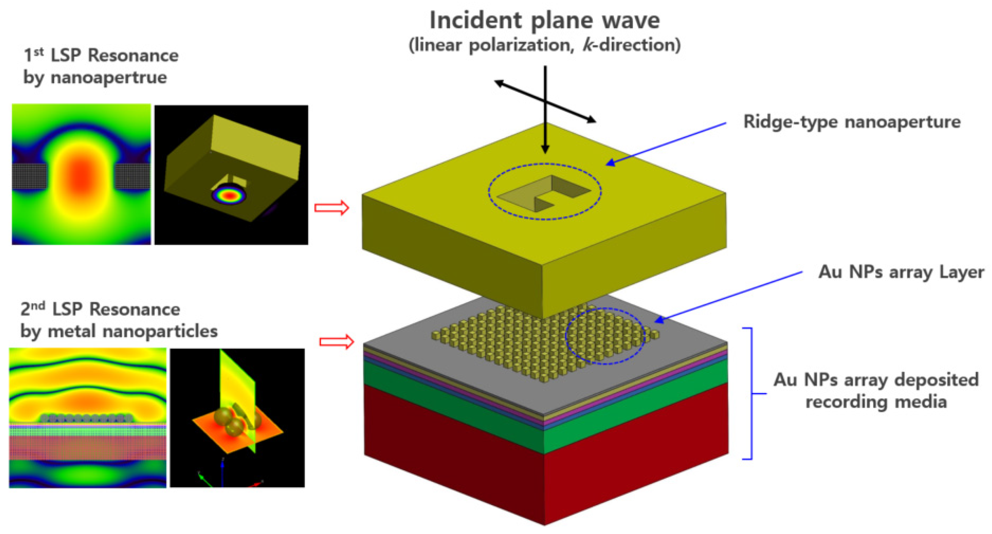
1. Introduction
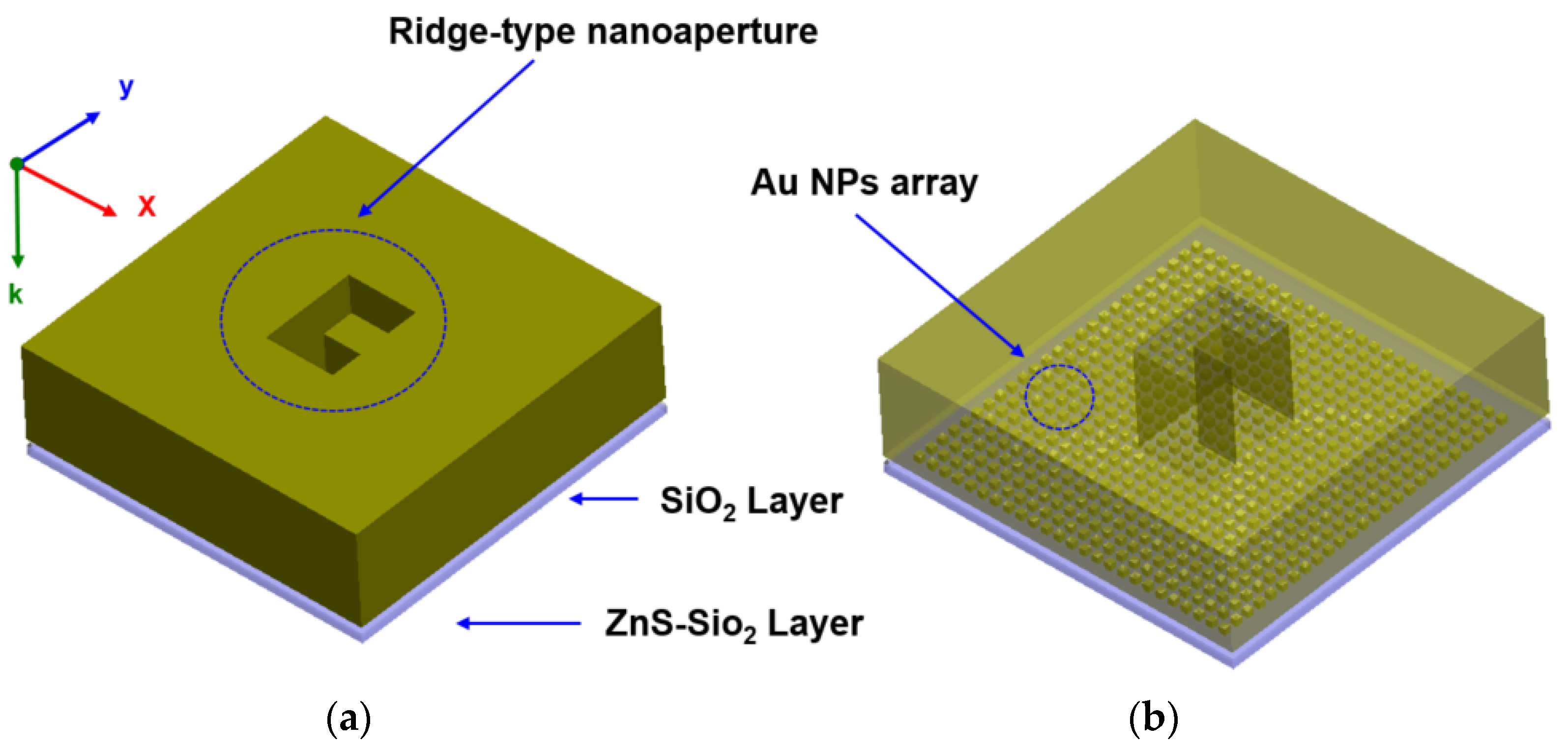
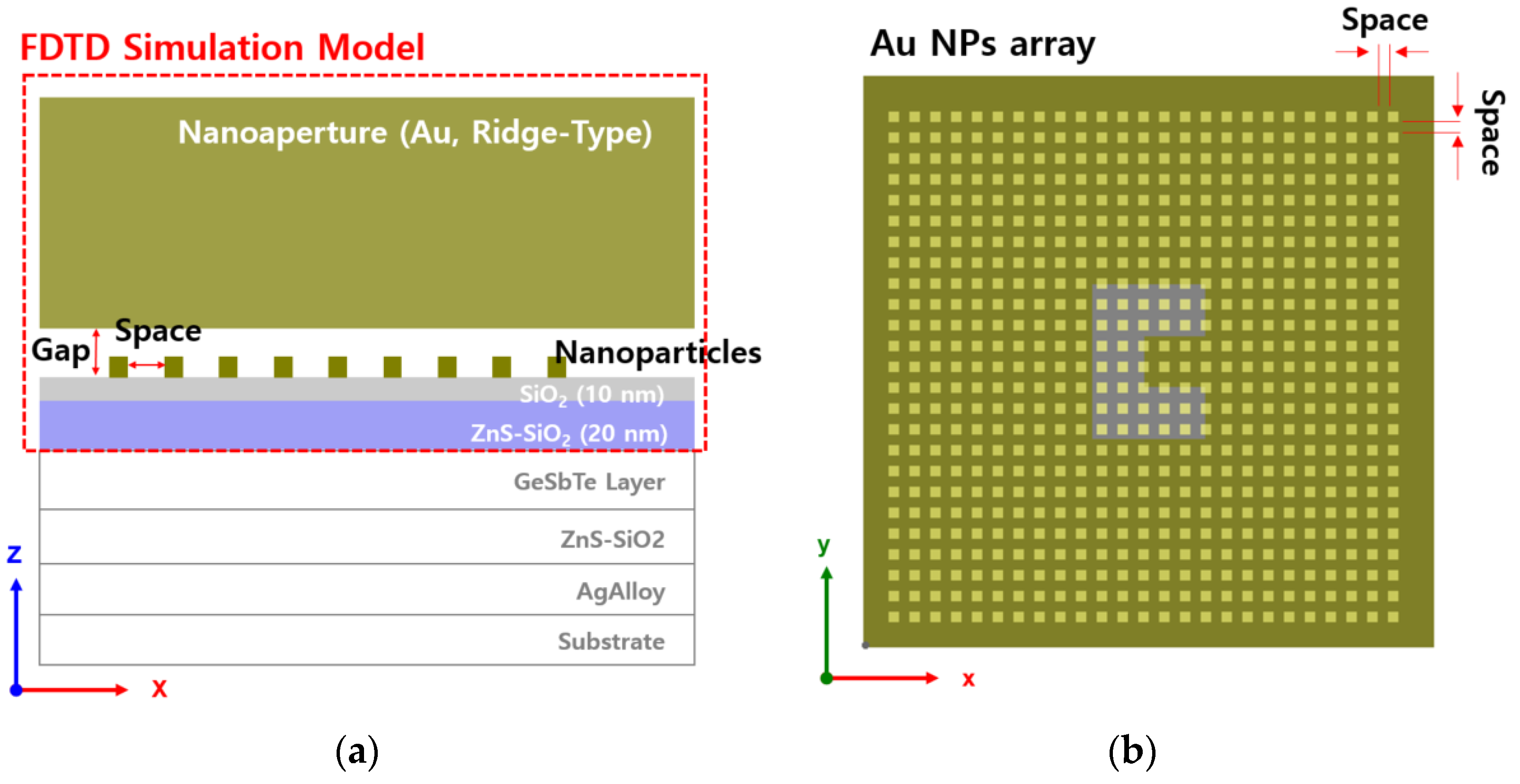
2. Modeling and Condition
3. Results and Discussion
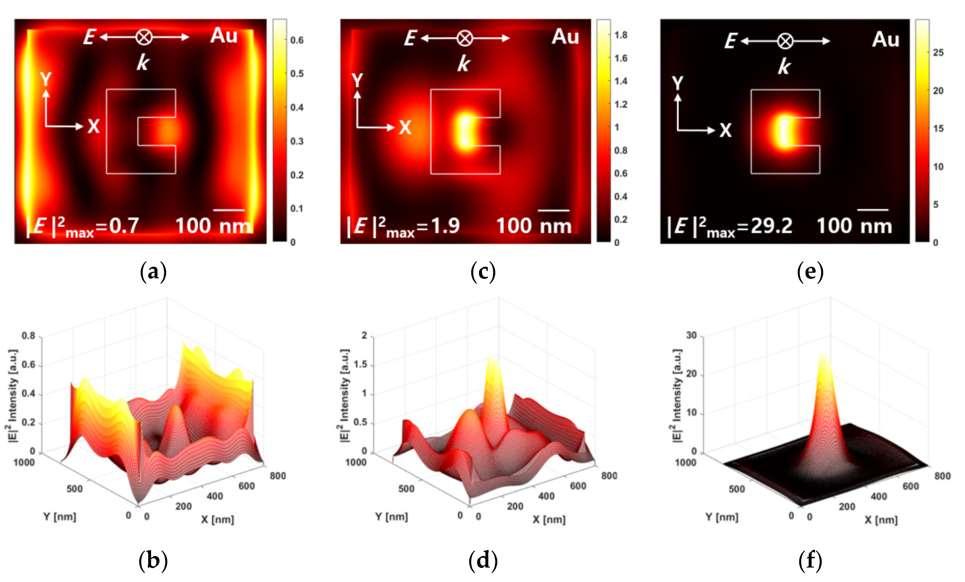
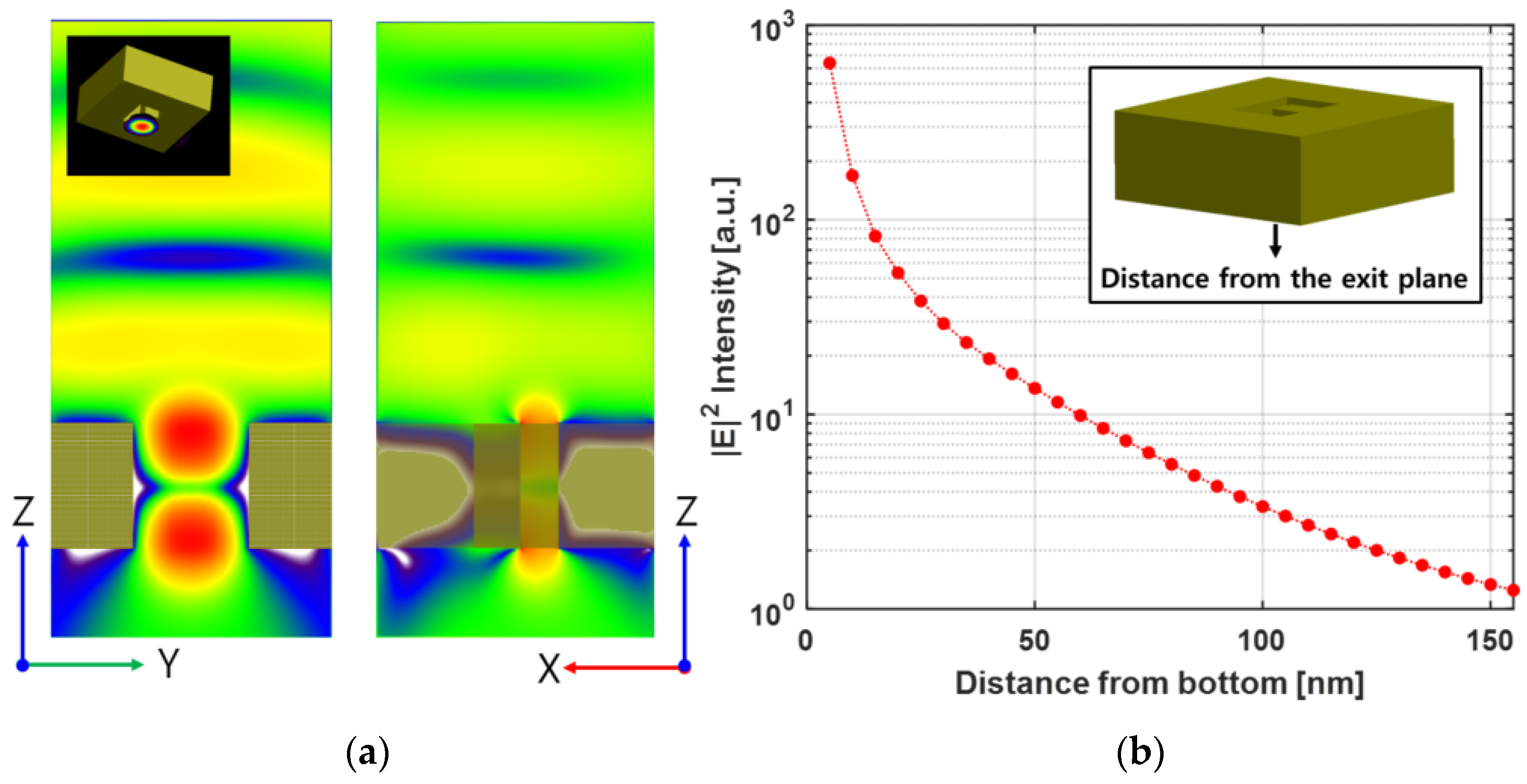
3.1. Performance Verification of Ridge-Type Nanoaperture
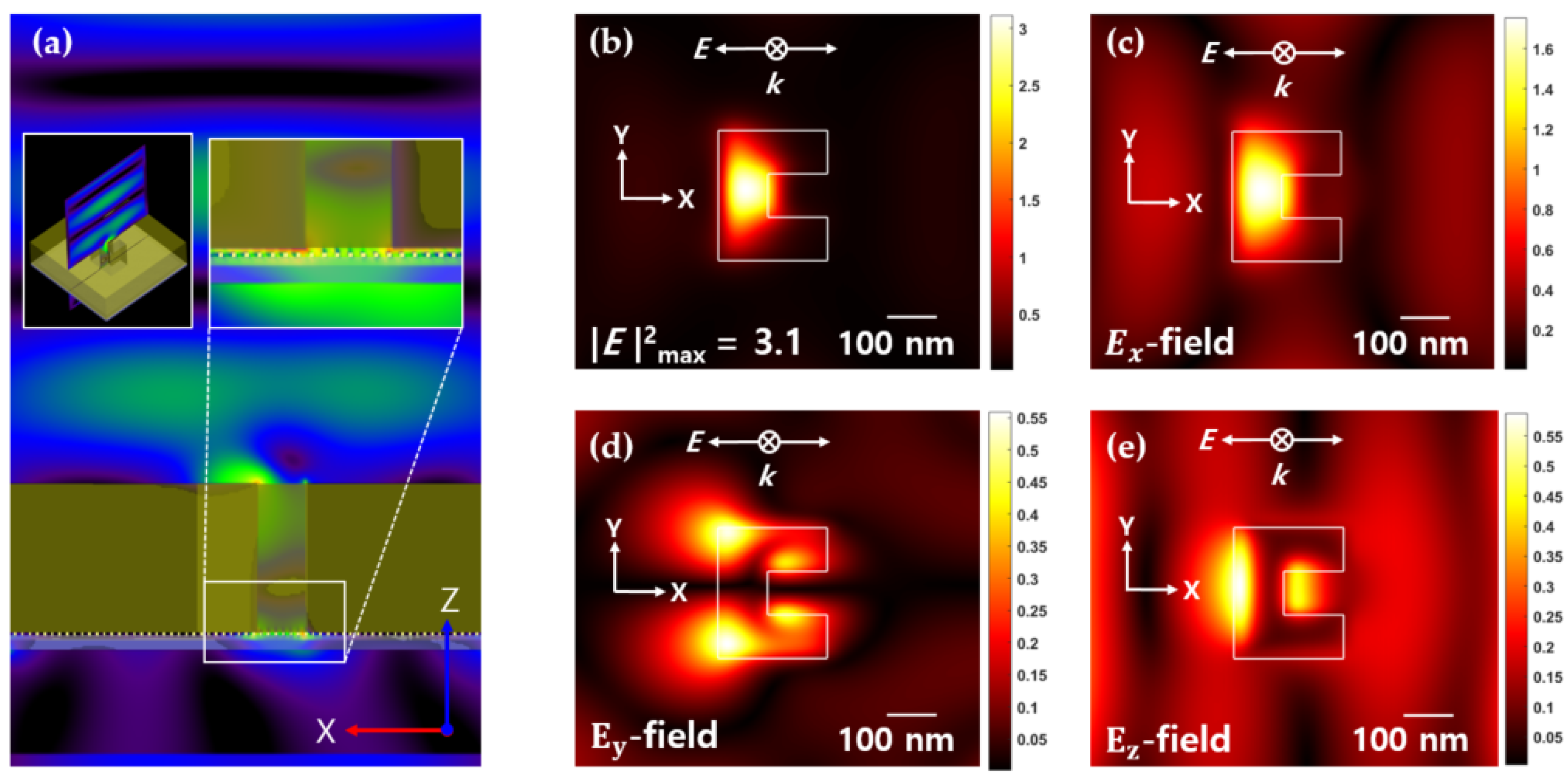
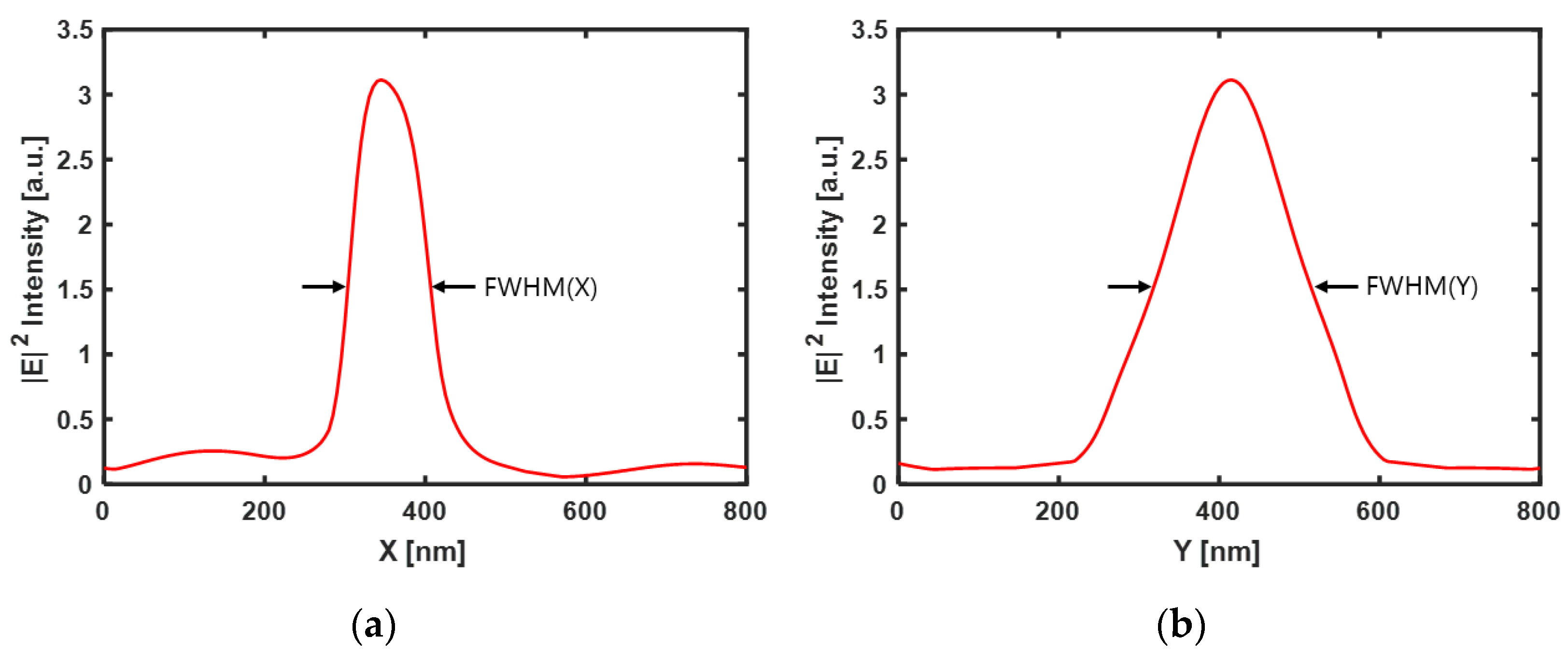
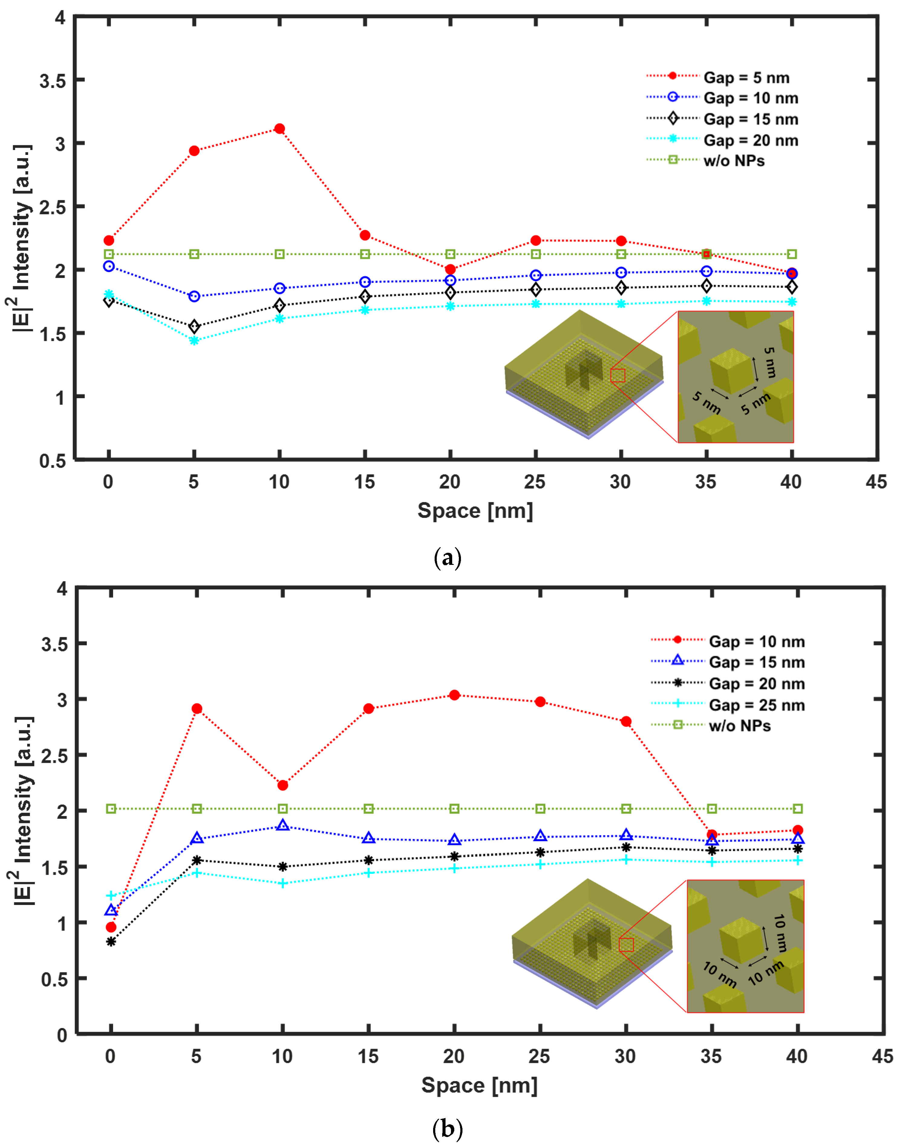
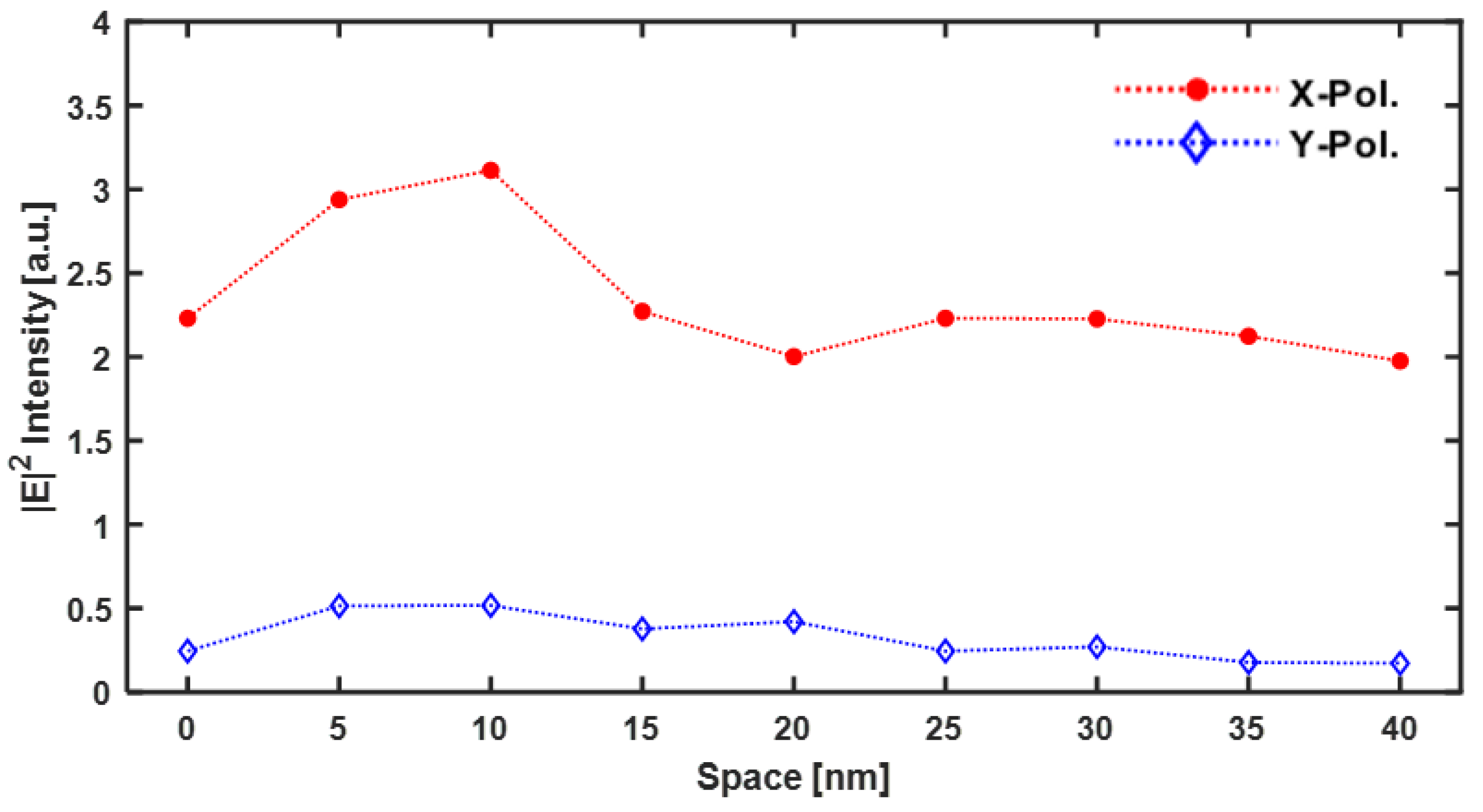
3.2. Nanopaterture and Au NPs Deposited Mdeia
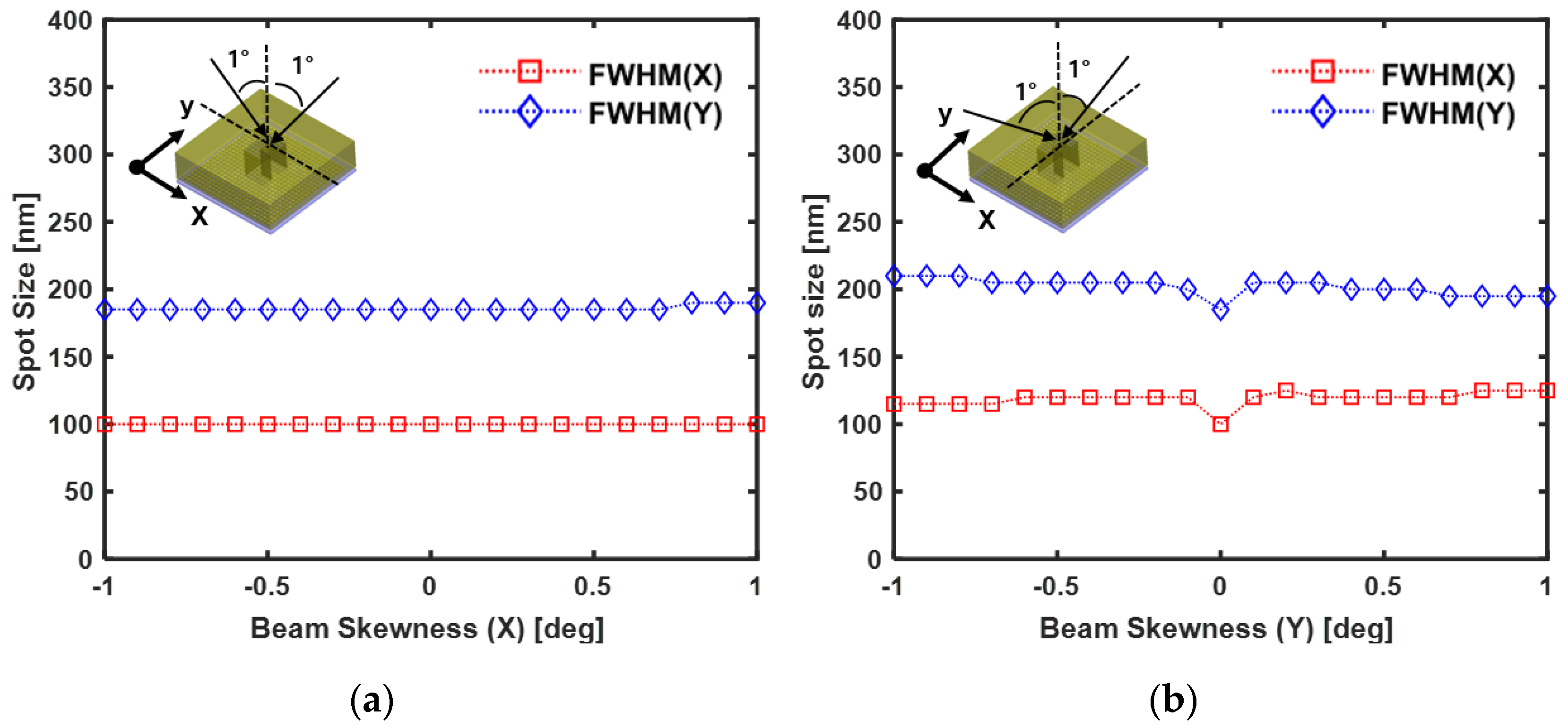
3.3. Polarization and Beam Skewness
4. Conclusions
Funding
Institutional Review Board Statement
Informed Consent Statement
Acknowledgments
Conflicts of Interest
References
- D’Aguanno, G.; Mattiucci, N.; Bloemer, M.J.; de Ceglia, D.; Vincenti, M.A.; Alù, A. Transmission resonances in plasmonic metallic gratings. J. Opt. Soc. Am. B 2011, 28, 253–264. [Google Scholar] [CrossRef]
- Byoungho, L.; Il-Min, L.; Seyoon, K.; Dong-Ho, O.; Lambertus, H. Review on subwavelength confinement of light with plasmonics. J. Mod. Opt. 2010, 57, 1479–1497. [Google Scholar]
- Stefan, A.M. Plasmonics: Metal Nanostructures for Subwavelength Photonic Devices. IEEE 2006, 12, 1214–1220. [Google Scholar]
- Hutter, E.; Fendler, J.H. Exploitation of Localized Surface Plasmon Resonance. Adv. Mater. 2004, 16, 1685–1706. [Google Scholar] [CrossRef]
- Capasso, F.; Yu, N.; Cubukcu, E.; Smythe, E. Using Plasmonics to Shape Light Beams. Opt. Photonics News 2009, 20, 22–27. [Google Scholar] [CrossRef]
- Barnes, W.L.; Dereux, A.; Ebbesen, T.W. Surface plasmon subwavelength optics. Nature 2003, 424, 824–830. [Google Scholar] [CrossRef]
- Kim, T.; Lee, W.-S.; Joe, H.-E.; Lim, G.; Choi, G.-J.; Gang, M.-G.; Kang, S.-M.; Park, K.-S.; Min, B.-K.; Park, Y.-P.; et al. High-speed plasmonic nanolithography with a solid immersion lens-based plasmonic optical head. Appl. Phys. Lett. 2012, 101, 161109. [Google Scholar] [CrossRef]
- Park, K.; Kim, T.; Lee, W.; Joe, H.; Min, B.; Park, Y.; Yang, H.; Kang, S.; Park, N. Application of Solid Immersion Lens-Based Near-Field Recording Technology to High-Speed Plasmonic Nanolithography. JJAP 2012, 51, 08JF01. [Google Scholar]
- Lee, W.; Kim, T.; Choi, G.; Lim, G.; Joe, H.; Gang, M.; Moon, H.; Kim, D.; Min, B.; Park, Y.; et al. Experimental demonstration of line-width modulation in plasmonic lithography using a solid immersion lens-based active nano-gap control. Appl. Phys. Lett. 2015, 106, 051111. [Google Scholar] [CrossRef]
- Kim, Y.; Kim, S.; Jung, H.; Lee, E.; Hahn, J.W. Plasmnic Nano lithography with a high scan speed contact probe. Opt. Express 2009, 17, 19476–19485. [Google Scholar] [CrossRef]
- Srituravanich, W.; Pan, L.; Wang, Y.; Sun, C.; Bogy, D.B.; Zhang, X. Flying plasmonic lens in the near field for high-speed nanolithography. Nat. Nanotechnol. 2008, 3, 733–737. [Google Scholar] [CrossRef] [PubMed]
- Mayer, K.M.; Hafner, J.H. Localized Surface Plasmon Resonance Sensors. Chem. Rev. 2011, 111, 3828–3857. [Google Scholar] [CrossRef] [PubMed]
- Eleonora, P.; Ulrich, J.K. Localized surface plasmon resonance: Nanostructures, bioassays and biosensing—A review. Anal. Chim. Acta 2011, 706, 8–24. [Google Scholar]
- Verellen, N.; Van Dorpe, P.; Huang, C.; Lodewijks, K.; Vandenbosch, G.A.; Lagae, L.; Moshchalkov, V.V. A Plasmon Line Shaping. Using Nanocrosses for High Sensitivity Localized Surface Plasmon Resonance Sensing. Nano Lett. 2011, 11, 391–397. [Google Scholar] [CrossRef] [PubMed]
- Kong, W.; Luo, Y.; Zhao, C.; Liu, L.; Gao, P.; Pu, M.; Wang, C.; Luo, X. Plasmonic Interference Lithography for Low-Cost Fabrication of Dense Lines with Sub-50 nm Half-Pitch. Appl. Nano Mater. 2019, 2, 489–496. [Google Scholar] [CrossRef]
- Chen, Y.; Ming, H. Review of surface plasmon resonance and localized surface plasmon resonance sensor. Photonic Sens. 2012, 2, 37–49. [Google Scholar] [CrossRef]
- Mandal, P.; Sharma, S. Progress in plasmonic solar cell efficiency improvement: A status review. Renew. Sustain. Energy Rev. 2016, 65, 537–552. [Google Scholar] [CrossRef]
- Jang, Y.H.; Jang, Y.J.; Kim, S.; Quan, L.N.; Chung, K.; Kim, D.H. Plasmonic Solar Cells: From Rational Design to Mechanism Overview. Chem. Rev. 2016, 116, 14982–15034. [Google Scholar] [CrossRef]
- Taya, S.A.; Al-Ashi, N.E.; Ramahi, O.M.; Colak, I.; Amiri, I.S. Surface plasmon resonance-based optical sensor using a thin layer of plasma. JOSA B 2021, 38, 2362–2367. [Google Scholar] [CrossRef]
- Taya, S.A.; Doghmosh, N.; Alkanoo, A.A.; Dhasarathan, V.; Ramanujam, N.R.; Amiri, I.S. Waveguides including negative permeability and simultaneously negative permittivity and permeability materials for sensing applications. Optik 2021, 228, 166147. [Google Scholar] [CrossRef]
- Hu, Y.; Meng, Y. Numerical modeling and analysis of plasmonic flying head for rotary near-field lithography technology. Friction 2018, 6, 443–456. [Google Scholar] [CrossRef]
- Pennacchio, A.; Ruggiero, G.; Staiano, M.; Piccialli, G.; Oliviero, G.; Lewkowicz, A.; Synak, A.; Bojarski, P.; D’Auria, S. A surface plasmon resonance based biochip for the detection of patulin toxin. Opt. Mater. 2014, 36, 1670–1675. [Google Scholar] [CrossRef]
- Wong, C.L.; Chua, M.; Mittman, H.; Choo, L.X.; Lim, H.Q.; Olivo, M. A Phase-Intensity Surface Plasmon Resonance Biosensor for Avian Influenza A (H5N1) Detection. Sensors 2017, 17, 2363. [Google Scholar] [CrossRef] [PubMed]
- Deng, Y.; Cao, G.; Wu, Y.; Zhou, X.; Liao, W. Theoretical Description of Dynamic Transmission Characteristics in MDM Waveguide Aperture-Side-Coupled with Ring Cavity. Plasmonics 2015, 10, 1537–1543. [Google Scholar] [CrossRef]
- Deng, Y.; Cao, G.; Yang, H.; Zhou, X.; Wu, Y. Dynamic Control of Double Plasmon-Induced Transparencies in Aperture-Coupled Waveguide-Cavity System. Plasmonics 2018, 13, 345–352. [Google Scholar] [CrossRef]
- Chen, H.; Chen, Z.; Yang, H.; Wenc, L.; Yi, Z.; Zhou, Z.; Dai, B.; Zhangd, J.; Wue, X.; Wu, P. Multi-mode surface plasmon resonance absorber based on dart-type single-layer graphene. RSC Adv. 2022, 12, 7821–7829. [Google Scholar] [CrossRef]
- Li, L.; Sun, X.; Xian, T.; Gao, H.; Wang, S.; Yi, Z.; Wue, X.; Yang, H. Template-free synthesis of Bi2O2CO3 hierarchical nanotubes self-assembled from ordered nanoplates for promising photocatalytic applications. Phys. Chem. Chem. Phys. 2022, 24, 8279–8295. [Google Scholar] [CrossRef]
- Bhirde, A.; Xie, J.; Swierczewska, M.; Chen, X. Nanoparticles for cell labeling. Nanoscale 2011, 3, 142–153. [Google Scholar] [CrossRef]
- Kang, S.M. Au Nanoparticle Array Deposited Phase-Change Material for Optical Information Recording Using Field Enhancement Based on Localized Surface Plasmon Resonance. Int. J. Precis. Eng. Manuf. 2019, 20, 267–272. [Google Scholar] [CrossRef]
- Sendur, K.; Challener, W. Near-field radiation of bow-tie antennas and apertures at optical frequencies. J. Microsc. 2003, 210, 279–283. [Google Scholar] [CrossRef]
- Jin, E.X.; Xu, X. Obtaining super resolution light spot using surface plasmon assisted sharp ridge nanoaperture. Appl. Phys. Lett. 2005, 86, 111106. [Google Scholar] [CrossRef]
- Guo, H.; Meyrath, T.P.; Zentgraf, T.; Liu, N.; Fu, L.; Schweizer, H.; Giessen, H. Optical resonances of bowtie slot antennas and their geometry and material dependence. Opt. Express 2008, 16, 7756–7766. [Google Scholar] [CrossRef] [PubMed]
- Kim, S.; Jin, J.; Kim, Y.-J.; Park, I.; Kim, Y.; Kim, S.-W. High-harmonic generation by resonant plasmon field enhancement. Nature 2008, 453, 757–760. [Google Scholar] [CrossRef] [PubMed]
- Tanaka, K.; Tanaka, M. Simulation of an aperture in the thick metallic screen that gives high intensity and small spot size using surface plasmon polariton. J. Microsc. 2003, 210, 294–300. [Google Scholar] [CrossRef] [PubMed]
- Jin, E.X.; Xu, X. Finite-Difference Time-Domain Studies on Optical Transmission through Planar Nano-Apertures in a Metal Film. Jpn. J. Appl. Phys. 2004, 43, 407–417. [Google Scholar] [CrossRef]
- Shi, X.; Hesselink, L.; Thornton, R.L. Ultrahigh light transmission through a C-shaped nanoaperture. Opt. Lett. 2003, 28, 1320–1322. [Google Scholar] [CrossRef]
- Itagi, A.V.; Stancil, D.D.; Bain, J.A.; Schlesinger, T.E. Ridge waveguide as a near-field optical source. Appl. Phys. Lett. 2003, 83, 4474–4476. [Google Scholar] [CrossRef]
- Ash, E.A.; Nicholls, G. Super-resolution Aperture Scanning Microscope. Nature 1972, 237, 510–512. [Google Scholar] [CrossRef]
- Pohl, D.W.; Denk, W.; Lanz, M. Optical stethoscopy: Image recording with resolution λ/20. Appl. Phys. Lett. 1984, 44, 651. [Google Scholar] [CrossRef]
- Lewis, A.; Isaacson, M.; Harootunian, A.; Muray, A. Development of a 500 Å spatial resolution light microscope: I. light is efficiently transmitted through λ/16 diameter apertures. Ultramicroscopy 1984, 13, 227–231. [Google Scholar] [CrossRef]
- Bethe, H.A. Theory of Diffraction by Small Holes. Phys. Rev. 1944, 66, 163. [Google Scholar] [CrossRef]
- Kunz, K.; Lubbers, R. The Finite Difference Time Domain Method for Electromagnetics; CRC Press: Boca Raton, FL, USA, 1996. [Google Scholar]
- XFDTD 6.4 Software; Remcom Inc.: State College, PA, USA, 2006.
- Kang, S.; Han, J.; Kim, T.; Park, N.; Park, K.; Min, B.; Park, Y. Multiple excitation of localized surface plasmon to create a 10 nm × 10 nm strong optical spot using an Au nanoparticle array-based ridge waveguide. Opt. Express 2010, 18, 1576–1585. [Google Scholar] [CrossRef] [PubMed]
- Palik, E.D. Handbook of Optical Constants of Solids; Academic Press: Orlando, FL, USA, 1996. [Google Scholar]
- Long, G.; Genga, Y. Investigation of ZnS–SiO2/Ag/ZnS–SiO2 as high stable transparent and conductive multilayer films. Appl. Surf. Sci. 2012, 263, 546–552. [Google Scholar] [CrossRef]


| Previous Study | Current Study | |
|---|---|---|
| Structure | NPs | NPs and Nanoaperture |
| Mechanism | LSP Resonance | Multiple LSP excitations |
| Beam | Focused beam | Plane wave |
| Wavelength | 405 nm, 658 nm, 780 nm | 780 nm |
| Efficiency | High | Very High |
| Resolution | ~λ/NA | FWHM (100 nm × 185 nm) |
| λ [nm] | Conductivity [S/m] | Relative Permittivity [Infinite Freq.] | Relaxation Time [s] | Static Permittivity |
|---|---|---|---|---|
| 405 | 294,500 | 1 | 6.9385 × 10⁻¹⁷ | −1.3078 |
| 658 | 3,162,200 | 1 | 3.7520 × 10⁻¹⁵ | −1339 |
| 780 | 7,854,100 | 1 | 6.0315 × 10⁻¹⁵ | −5349.2 |
| Material | Conductivity [S/m] | Relative Permittivity [Infinite Freq.] | Relaxation Time [s] | Static Permittivity |
|---|---|---|---|---|
| SiO2 | 785,980 | 1 | −3.4189 × 10⁻¹⁶ | 31.3487 |
| ZnS–SiO2 | 15,383,000 | 1 | 6.8779 × 10⁻¹⁵ | −11,948 |
Publisher’s Note: MDPI stays neutral with regard to jurisdictional claims in published maps and institutional affiliations. |
© 2022 by the author. Licensee MDPI, Basel, Switzerland. This article is an open access article distributed under the terms and conditions of the Creative Commons Attribution (CC BY) license (https://creativecommons.org/licenses/by/4.0/).
Share and Cite
Kang, S.-M. Study of Optical Information Recording Mechanism Based on Localized Surface Plasmon Resonance with Au Nanoparticles Array Deposited Media and Ridge-Type Nanoaperture. Nanomaterials 2022, 12, 1350. https://doi.org/10.3390/nano12081350
Kang S-M. Study of Optical Information Recording Mechanism Based on Localized Surface Plasmon Resonance with Au Nanoparticles Array Deposited Media and Ridge-Type Nanoaperture. Nanomaterials. 2022; 12(8):1350. https://doi.org/10.3390/nano12081350
Chicago/Turabian StyleKang, Sung-Mook. 2022. "Study of Optical Information Recording Mechanism Based on Localized Surface Plasmon Resonance with Au Nanoparticles Array Deposited Media and Ridge-Type Nanoaperture" Nanomaterials 12, no. 8: 1350. https://doi.org/10.3390/nano12081350
APA StyleKang, S.-M. (2022). Study of Optical Information Recording Mechanism Based on Localized Surface Plasmon Resonance with Au Nanoparticles Array Deposited Media and Ridge-Type Nanoaperture. Nanomaterials, 12(8), 1350. https://doi.org/10.3390/nano12081350