
MOVPE Growth of GaN via Graphene Layers on GaN/Sapphire Templates

 , , ,
, , , 
Abstract
1. Introduction
2. Materials and Methods
3. Results and Discussion
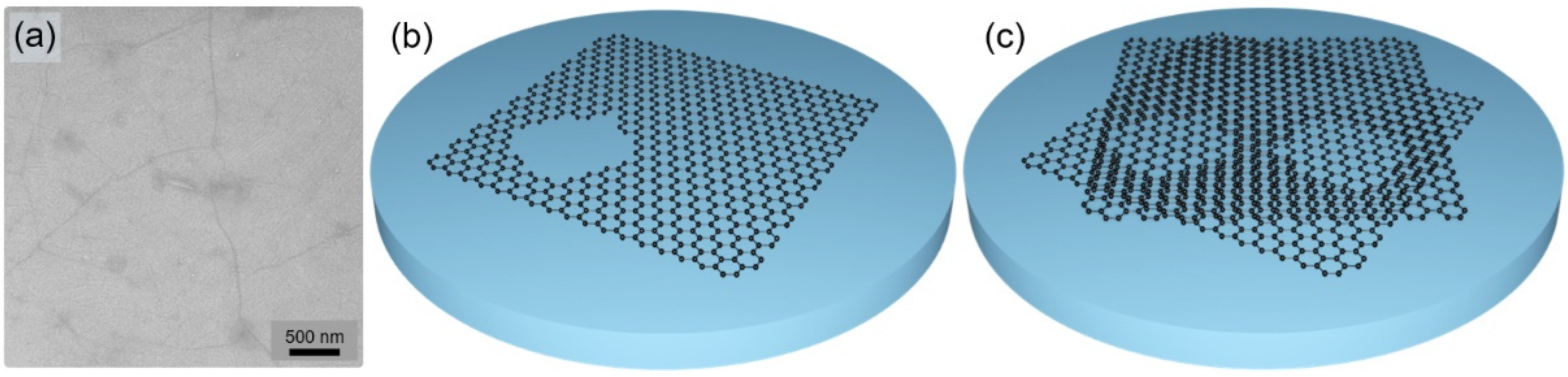
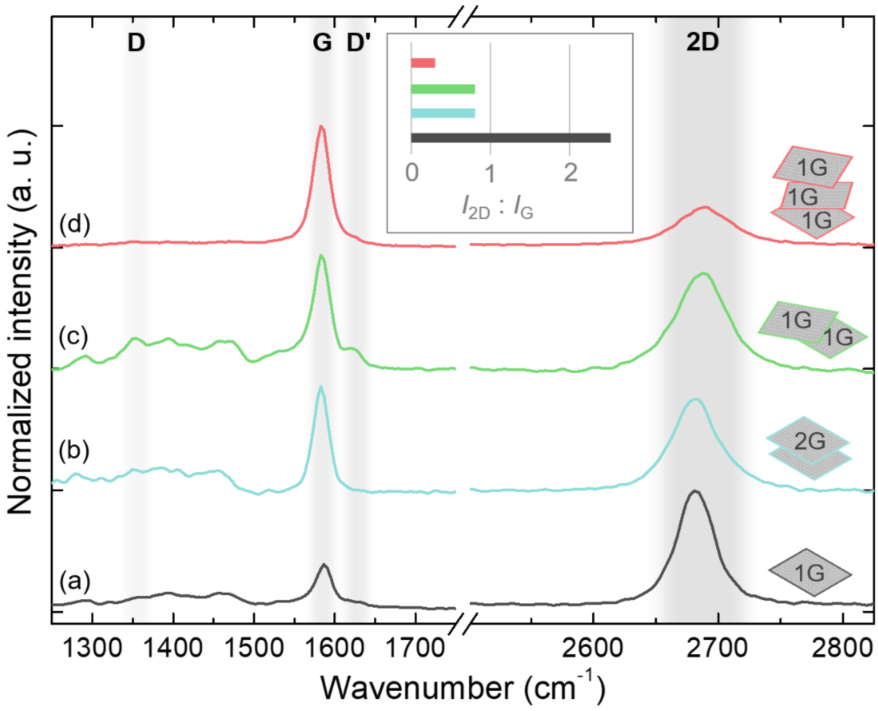
3.1. Graphene Layer Transfer
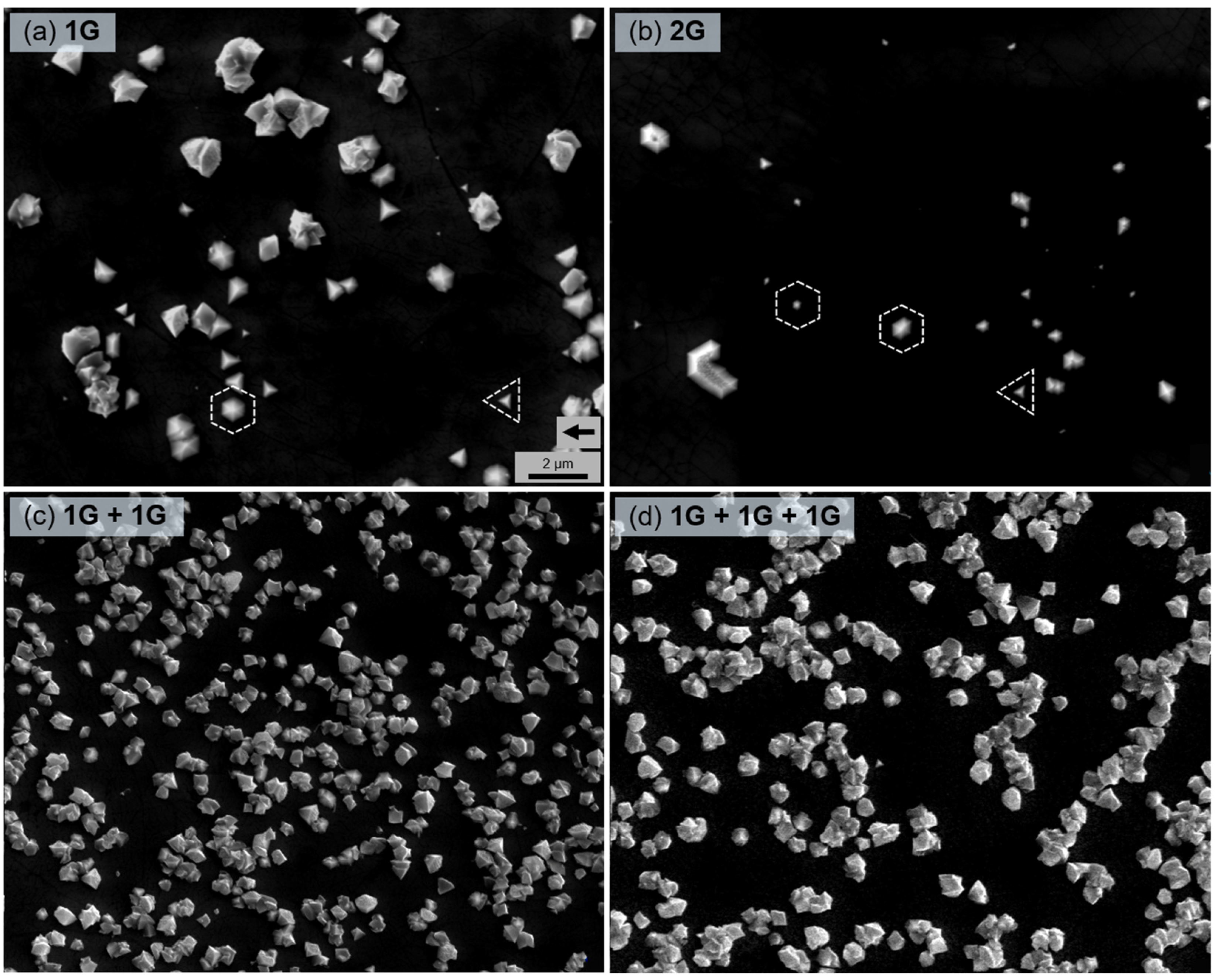
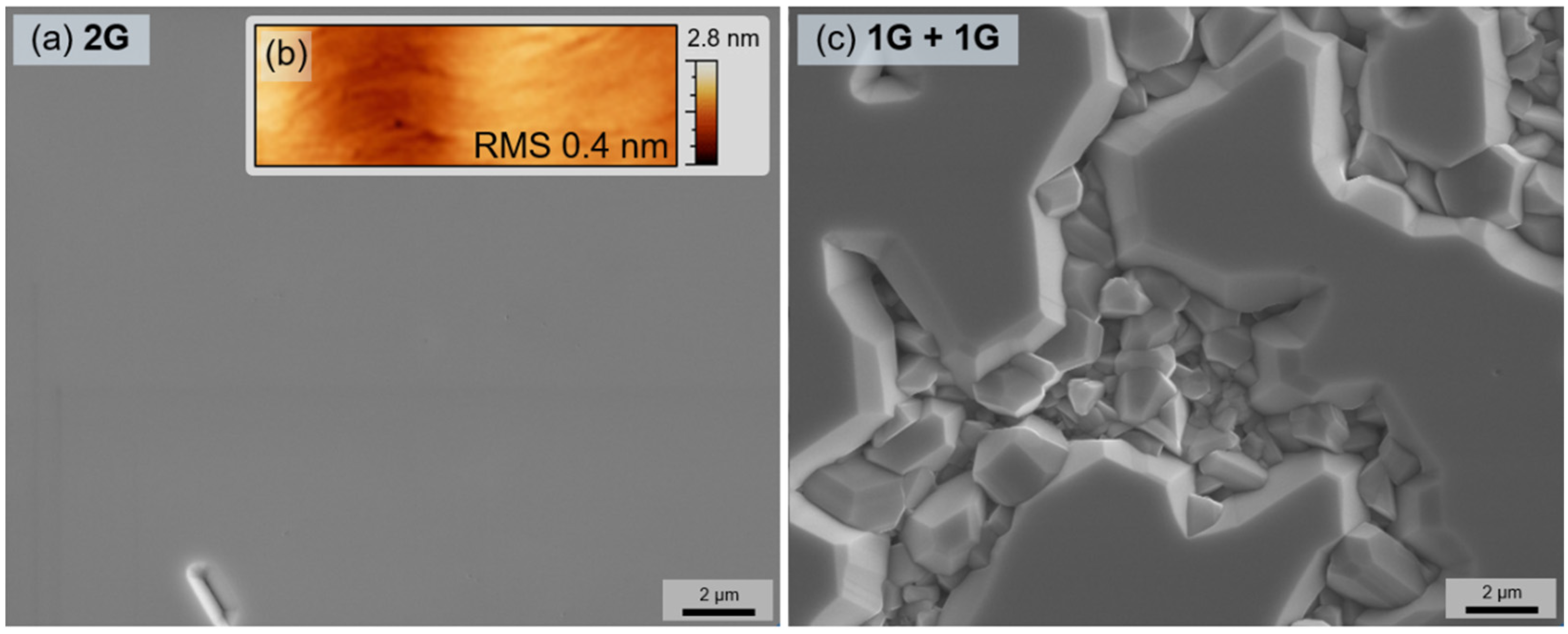
3.2. Growth of GaN Epilayers
3.3. Exfoliation of GaN Epilayer
4. Conclusions
Author Contributions
Funding
Institutional Review Board Statement
Informed Consent Statement
Data Availability Statement
Conflicts of Interest
References
- Bae, S.-H.; Kum, H.; Kong, W.; Kim, Y.; Choi, C.; Lee, B.; Lin, P.; Park, Y.; Kim, J. Integration of bulk materials with two-dimensional materials for physical coupling and applications. Nat. Mater. 2019, 18, 550–560. [Google Scholar] [CrossRef] [PubMed]
- Yu, J.; Wang, L.; Hao, Z.; Luo, Y.; Sun, C.; Wang, J.; Han, Y.; Xiong, B.; Li, H. Van der Waals Epitaxy of III-Nitride Semiconductors Based on 2D Materials for Flexible Applications. Adv. Mater. 2020, 32, 1903407. [Google Scholar] [CrossRef]
- Liang, D.; Wei, T.; Wang, J.; Li, J. Quasi van der Waals epitaxy nitride materials and devices on two dimension materials. Nano Energy 2020, 69, 104463. [Google Scholar] [CrossRef]
- Alaskar, Y.; Arafin, S.; Wickramaratne, D.; Zurbuchen, M.A.; He, L.; McKay, J.; Lin, Q.; Goorsky, M.S.; Lake, R.K.; Wang, K.L. Towards van der Waals Epitaxial Growth of GaAs on Si using a Graphene Buffer Layer. Adv. Funct. Mater. 2014, 24, 6629–6638. [Google Scholar] [CrossRef]
- Chang, H.; Liu, B.; Liang, D.; Gao, Y.; Yan, J.; Liu, Z.; Liu, Z.; Wang, J.; Li, J.; Gao, P.; et al. Graphene-induced crystal-healing of AlN film by thermal annealing for deep ultraviolet light-emitting diodes. Appl. Phys. Lett. 2020, 117, 181103. [Google Scholar] [CrossRef]
- Chen, Z.; Liu, Z.; Wei, T.; Yang, S.; Dou, Z.; Wang, Y.; Ci, H.; Chang, H.; Qi, Y.; Yan, J.; et al. Improved Epitaxy of AlN Film for Deep-Ultraviolet Light-Emitting Diodes Enabled by Graphene. Adv. Mater. 2019, 31, 1807345. [Google Scholar] [CrossRef]
- He, S.; Xu, Y.; Qi, L.; Li, Z.; Cao, B.; Wang, C.; Zhang, J.; Wang, J.; Xu, K. Growth of low-threading-dislocation-density GaN on graphene by hydride vapor phase epitaxy. Jpn. J. Appl. Phys. 2017, 56, 030308. [Google Scholar] [CrossRef]
- Kim, J.; Bayram, C.; Park, H.; Cheng, C.-W.; Dimitrakopoulos, C.; Ott, J.A.; Reuter, K.B.; Bedell, S.W.; Sadana, D.K. Principle of direct van der Waals epitaxy of single-crystalline films on epitaxial graphene. Nat. Commun. 2014, 5, 4836. [Google Scholar] [CrossRef]
- Qiao, K.; Liu, Y.; Kim, C.; Molnar, R.J.; Osadchy, T.; Li, W.; Sun, X.; Li, H.; Myers-Ward, R.L.; Lee, D.; et al. Graphene Buffer Layer on SiC as a Release Layer for High-Quality Freestanding Semiconductor Membranes. J. Nano Lett. 2021, 21, 4013–4020. [Google Scholar] [CrossRef]
- Kim, Y.; Cruz, S.S.; Lee, K.; Alawode, B.O.; Choi, C.; Song, Y.; Johnson, J.M.; Heidelberger, C.; Kong, W.; Choi, S.; et al. Remote epitaxy through graphene enables two-dimensional material-based layer transfer. Nature 2017, 544, 340–343. [Google Scholar] [CrossRef]
- Kong, W.; Li, H.; Qiao, K.; Kim, Y.; Lee, K.; Nie, Y.; Lee, D.; Osadchy, T.; Molnar, R.J.; Gaskill, D.K.; et al. Polarity governs atomic interaction through two-dimensional materials. Nat. Mater. 2018, 17, 999–1004. [Google Scholar] [CrossRef] [PubMed]
- Jeong, J.; Wang, Q.; Cha, J.; Jin, D.K.; Shin, D.H.; Kwon, S.; Kang, B.K.; Jang, J.H.; Yang, W.S.; Choi, Y.S.; et al. Remote heteroepitaxy of GaN microrod heterostructures for deformable light-emitting diodes and wafer recycle. J. Sci. Adv. 2020, 6, eaaz5180. [Google Scholar] [CrossRef] [PubMed]
- Wang, D.; Lu, Y.; Meng, J.; Zhang, X.; Yin, Z.; Gao, M.; Wang, Y.; Cheng, L.; You, J.; Zhang, J. Remote heteroepitaxy of atomic layered hafnium disulfide on sapphire through hexagonal boron nitride. Nanoscale 2019, 11, 9310. [Google Scholar] [CrossRef] [PubMed]
- Jiang, J.; Sun, X.; Chen, X.; Wang, B.; Chen, Z.; Hu, Y.; Guo, Y.; Zhang, L.; Ma, Y.; Gao, L.; et al. Carrier lifetime enhancement in halide perovskite via remote epitaxy. Nat. Commun. 2019, 10, 4145. [Google Scholar] [CrossRef]
- Guo, Y.; Sun, X.; Jiang, J.; Wang, B.; Chen, X.; Yin, X.; Qi, W.; Gao, L.; Zhang, L.; Lu, Z.; et al. A Reconfigurable Remotely Epitaxial VO2 Electrical Heterostructure. Nano Lett. 2020, 20, 33–42. [Google Scholar] [CrossRef]
- Su, J.; Liang, D.; Zhao, Y.; Yang, J.; Chang, H.; Duan, R.; Wang, J.; Sun, L.; Wei, T. Freestanding GaN substrate enabled by dual-stack multilayer graphene via hydride vapor phase epitaxy. Appl. Surf. Sci. 2020, 526, 146747. [Google Scholar] [CrossRef]
- Deng, Z.; Wang, X. Strain engineering on the electronic states of two-dimensional GaN/graphene heterostructure. RSC Adv. 2019, 9, 26024. [Google Scholar] [CrossRef]
- Xu, Y.; Cao, B.; Li, Z.; Cai, D.; Zhang, Y.; Ren, G.; Wang, J.; Shi, L.; Wang, C.; Xu, K. Growth Model of van der Waals Epitaxy of Films: A Case of AlN Films on Multilayer Graphene/SiC. ACS Appl. Mater. Interfaces 2017, 9, 44001. [Google Scholar] [CrossRef]
- Ullah, S.; Yang, X.; Ta, H.Q.; Hasan, M.; Bachmatiuk, A.; Tokarska, K.; Trzebicka, B.; Fu, L.; Rummeli, M.H. Graphene transfer methods: A review. Nano Res. 2021, 14, 3756–3772. [Google Scholar] [CrossRef]
- Song, Y.; Zou, W.; Lu, Q.; Lin, L.; Liu, Z. Graphene Transfer: Paving the Road for Applications of Chemical Vapor Deposition Graphene. Small 2021, 17, 2007600. [Google Scholar] [CrossRef]
- Kim, H.; Lu, K.; Liu, Y.; Kum, H.S.; Kim, K.S.; Qiao, K.; Bae, S.-H.; Lee, S.; Ji, Y.J.; Kim, K.H.; et al. Impact of 2D–3D Heterointerface on Remote Epitaxial Interaction through Graphene. ACS Nano 2021, 15, 10587–10596. [Google Scholar] [CrossRef]
- Zhang, L.; Li, X.; Shao, Y.; Yu, J.; Wu, Y.; Hao, X.; Yin, Z.; Dai, Y.; Tian, Y.; Huo, Q.; et al. Improving the quality of GaN crystals by using graphene or hexagonal boron nitride nanosheets substrate. ACS Appl. Mater. Interfaces 2015, 7, 4504–4510. [Google Scholar] [CrossRef] [PubMed]
- Lee, J.-Y.; Min, J.-H.; Bae, S.-Y.; Park, M.-D.; Jeong, W.-L.; Park, J.-H.; Kang, C.-M.; Lee, D.-S. Multiple epitaxial lateral overgrowth of GaN thin films using a patterned graphene mask by metal organic chemical vapor deposition. J. Appl. Cryst. 2020, 53, 1502–1508. [Google Scholar] [CrossRef]
- Horcas, I.; Fernandez, R.; Gomez-Rodriguez, J.M.; Colchero, J.; Gomez-Herrero, J.; Baro, A.M. WSXM: A software for scanning probe microscopy and a tool for nanotechnology. Rev. Sci. Instrum. 2007, 78, 013705. [Google Scholar] [CrossRef] [PubMed]
- Badokas, K.; Kadys, A.; Mickevičius, J.; Ignatjev, I.; Skapas, M.; Stanionytė, S.; Radiunas, E.; Juška, G.; Malinauskas, T. Remote epitaxy of GaN via graphene on GaN/sapphire templates. J. Phys. D Appl. Phys. 2021, 54, 205103. [Google Scholar] [CrossRef]
- Haboeck, U.; Siegle, H.; Hoffmann, A.; Thomsen, C. Lattice dynamics in GaN and AlN probed with first- and second-order Raman spectroscopy. Phys. Status Solidi C 2003, 0, 1710–1731. [Google Scholar] [CrossRef][Green Version]
- Davydov, V.Y.; Kitaev, Y.E.; Goncharuk, I.N.; Smirnov, A.N.; Graul, J.; Semchinova, O.; Uffmann, D.; Smirnow, M.B.; Mirgorodsky, A.P.; Evarestov, R.A. Phonon dispersion and Raman scattering in hexagonal GaN and AlN. Phys. Rev. B 1998, 58, 12899. [Google Scholar] [CrossRef]
- Bleu, Y.; Bourquard, F.; Loir, A.-S.; Barnier, V.; Garrelie, F.; Donnet, C. Raman study of the substrate influence on graphene synthesis using a solid carbon source via rapid thermal annealing. J. Raman Spectrosc. 2019, 50, 1630. [Google Scholar] [CrossRef]
- Ferrari, A.C.; Meyer, J.C.; Scardaci, V.; Casiraghi, C.; Lazzeri, M.; Mauri, F.; Piscanec, S.; Jiang, D.; Novoselov, K.S.; Roth, S.; et al. Raman Spectrum of Graphene and Graphene Layers. Phys. Rev. Lett. 2006, 97, 187401. [Google Scholar] [CrossRef]
- Malard, L.M.; Pimenta, M.A.; Dresselhaus, G.; Dresselhaus, M.S. Raman spectroscopy in graphene. Phys. Rep. 2009, 473, 51–87. [Google Scholar] [CrossRef]
- Mun, D.-H.; Bae, H.; Bae, S.; Lee, H.; Ha, J.-S.; Lee, S. Stress relaxation of GaN microstructures on a graphene-buffered Al2O3 substrate. Phys. Status Solidi RRL 2014, 8, 341–344. [Google Scholar] [CrossRef]
- Wang, S.; Zhang, Y.; Abidi, N.; Cabrales, L. Wettability and Surface Free Energy of Graphene Films. Langmuir 2009, 25, 11078–11081. [Google Scholar] [CrossRef] [PubMed]
- Liu, F.; Zhang, Z.; Rong, X.; Yu, Y.; Wang, T.; Sheng, B.; Wei, J.; Zhou, S.; Yang, X.; Xu, F.; et al. Graphene-Assisted Epitaxy of Nitrogen Lattice Polarity GaN Films on Non-Polar Sapphire Substrates for Green Light Emitting Diodes. Adv. Funct. Mater. 2020, 30, 2001283. [Google Scholar] [CrossRef]
- Al Balushi, Z.Y.; Miyagi, T.; Lin, Y.-C.; Wang, K.; Calderin, L.; Bhimanapati, G.; Redwing, J.M.; Robinson, J.A. The impact of graphene properties on GaN and AlN nucleation. Surf. Sci. 2015, 634, 81–88. [Google Scholar] [CrossRef]
- Lundin, W.V.; Zavarin, E.E.; Sakharov, A.V.; Zakheim, D.A.; Davydov, V.Y.; Smirnov, A.N.; Eliseyev, I.A.; Yagovkina, M.A.; Brunkov, P.N.; Lundina, E.Y.; et al. Growth of III-N/graphene heterostructures in single vapor phase epitaxial process. J. Cryst. Growth 2018, 504, 1–6. [Google Scholar] [CrossRef]
- Bedell, S.W.; Lauro, P.; Ott, J.A.; Fogel, K.; Sadana, D.K. Layer transfer of bulk gallium nitride by controlled spalling. J. Appl. Phys. 2017, 122, 025103. [Google Scholar] [CrossRef]
- Park, J.-H.; Lee, J.-Y.; Park, M.-D.; Min, J.-H.; Lee, J.-S.; Yang, X.; Kang, S.; Kim, S.-J.; Jeong, W.-L.; Amano, H.; et al. Influence of temperature-dependent substrate decomposition on graphene for separable GaN growth. Adv. Mater. Interfaces 2019, 6, 1900821. [Google Scholar] [CrossRef]


Publisher’s Note: MDPI stays neutral with regard to jurisdictional claims in published maps and institutional affiliations. |
© 2022 by the authors. Licensee MDPI, Basel, Switzerland. This article is an open access article distributed under the terms and conditions of the Creative Commons Attribution (CC BY) license (https://creativecommons.org/licenses/by/4.0/).
Share and Cite
Badokas, K.; Kadys, A.; Augulis, D.; Mickevičius, J.; Ignatjev, I.; Skapas, M.; Šebeka, B.; Juška, G.; Malinauskas, T. MOVPE Growth of GaN via Graphene Layers on GaN/Sapphire Templates. Nanomaterials 2022, 12, 785. https://doi.org/10.3390/nano12050785
Badokas K, Kadys A, Augulis D, Mickevičius J, Ignatjev I, Skapas M, Šebeka B, Juška G, Malinauskas T. MOVPE Growth of GaN via Graphene Layers on GaN/Sapphire Templates. Nanomaterials. 2022; 12(5):785. https://doi.org/10.3390/nano12050785
Chicago/Turabian StyleBadokas, Kazimieras, Arūnas Kadys, Dominykas Augulis, Jūras Mickevičius, Ilja Ignatjev, Martynas Skapas, Benjaminas Šebeka, Giedrius Juška, and Tadas Malinauskas. 2022. "MOVPE Growth of GaN via Graphene Layers on GaN/Sapphire Templates" Nanomaterials 12, no. 5: 785. https://doi.org/10.3390/nano12050785
APA StyleBadokas, K., Kadys, A., Augulis, D., Mickevičius, J., Ignatjev, I., Skapas, M., Šebeka, B., Juška, G., & Malinauskas, T. (2022). MOVPE Growth of GaN via Graphene Layers on GaN/Sapphire Templates. Nanomaterials, 12(5), 785. https://doi.org/10.3390/nano12050785