Article

Magnetotransport Studies of Encapsulated Topological Insulator Bi2Se3 Nanoribbons

1
Institute of Chemical Physics, University of Latvia, 19 Raina Blvd., LV-1586 Riga, Latvia
2
Research and Development Department, Integrated Micro- and Nanosystems, Belarusian State University of Informatics and Radioelectronics, P. Brovki Str. 6, 220013 Minsk, Belarus
3
Institut Européen des Membranes, IEM, UMR 5635, University of Montpellier, ENSCM, CNRS, 34095 Montpellier, France
4
Institute of Solid State Physics, University of Latvia, Kengaraga 8, LV-1063 Riga, Latvia
5
Quantum Device Physics Laboratory, Department of Microtechnology and Nanoscience, Chalmers University of Technology, SE-41296 Goteborg, Sweden
*
Author to whom correspondence should be addressed.
Nanomaterials 2022, 12(5), 768; https://doi.org/10.3390/nano12050768
Submission received: 27 January 2022 / Revised: 18 February 2022 / Accepted: 20 February 2022 / Published: 24 February 2022
(This article belongs to the Topic Synthesis and Applications of Nanowires)

Abstract

:
The majority of proposed exotic applications employing 3D topological insulators require high-quality materials with reduced dimensions. Catalyst-free, PVD-grown Bi2Se3 nanoribbons are particularly promising for these applications due to the extraordinarily high mobility of their surface Dirac states, and low bulk carrier densities. However, these materials are prone to the formation of surface accumulation layers; therefore, the implementation of surface encapsulation layers and the choice of appropriate dielectrics for building gate-tunable devices are important. In this work, all-around ZnO-encapsulated nanoribbons are investigated. Gate-dependent magnetotransport measurements show improved charge transport characteristics as reduced nanoribbon/substrate interface carrier densities compared to the values obtained for the as-grown nanoribbons on SiO2 substrates.

1. Introduction

Three-dimensional topological insulators (3D-TIs) are among the major materials in the class of topological materials. 3D-TIs have attracted significant research interest due to their unusual surface properties. Carriers originating from topological surface states exhibit a Dirac cone in the band structure [1] and charge transport via these states is protected against backscattering from non-magnetic impurities [2,3]. If proximitized with an s-wave superconductor, superconductivity induced in the topological surface states is unconventional and predicted to host Majorana fermions [4,5]. The exploitation of these exotic surface properties is advantageous for a variety of applications, for example, in topological quantum computing [6], spintronics [7,8], and in the development of new-concept electronic devices [9]. The surface states of TIs are metallic while the bulk of the material, which is expected to be an insulator, is highly doped due to the formation of native defects [10]. This aspect remains the main challenge in accessing the surface-state charge transport, hampering progress towards the development of applications beyond fundamental studies.
Owing to their large surface-to-volume ratio, 3D-TI nanowires and nanoribbons are promising candidates with which to achieve truly topological surface-state-dominated charge transport without any contribution from the bulk. Their nanosized geometry provides even more functionalities because of the low number of transport modes [11], which is particularly important for probing Majorana states [6]. Remarkable improvements in material quality have been demonstrated in 3D-TIs doped with native-defect-compensating substitutions. Nearly insulating bulk with a charge carrier density of ~1015 cm−3 has been reported in single crystals of BiSbTeSe2 [12] (BSTS), but this approach is not fully successful in nanowires and nanoribbons. Here, precise and reproducible concentrations of dopants are challenging to obtain, and they are achieved at the expense of charge carrier mobility [13].
Nanoribbons of Bi2Se3 have been reported to be nearly ideal 3D-TIs, practically without any bulk conduction, and with exceptionally high carrier mobilities [14,15]. However, Bi2Se3 is prone to the formation of surface accumulation layers [16]; this is particularly evident in thin nanoribbons, where the thickness is comparable with the Debye screening length [14,17,18]. The majority of the proposed 3D-TI-nanoribbon-based electronic devices require good tunability of their chemical potential for accessing surface Dirac carriers in a controlled manner. This can be achieved by employing electrostatic gating techniques. However, additional trivial carriers with large densities form at the nanoribbon surfaces, or at the interface with the substrate, which cannot be effectively depleted by common electrostatic gating techniques. Therefore, more effort is needed to prevent the uncontrolled formation of surface accumulation layers in Bi2Se3 nanoribbons.
The use of surface-capping layers for Bi2Se3 and Bi2Te3 has proven to be beneficial to protect against environmental doping [19] and to probe surface state transport. Widely used capping layer materials are Te or Se, and the oxide layers of ZnO or Al2O3 [13,20,21], deposited on the top surface of the material. This allows more efficient electrostatic tuning of the Fermi level [21], while in the case of Bi2Se3 nanoribbons, where the accumulation layer is formed at the nanoribbon/substrate interface [14,17], other approaches have to be considered.
In this work, we used atomic layer deposition (ALD) to fabricate all-around ZnO-capped or -encapsulated Bi2Se3 nanoribbons. The choice of selecting ZnO as an encapsulation layer material was based on the fact that thin layers of high-quality ZnO are possible to grow at moderate temperatures. This is particularly important for preserving the stoichiometry of Bi2Se3, as elevated temperatures may cause the unwanted out-diffusion of Se, which increases the doping of the bulk. Comparative magnetotransport studies of individual encapsulated and as-grown Bi2Se3 nanoribbons from the same batch synthesis show that the encapsulation layer of ZnO helps to minimize the impact of the accumulation layer at the nanoribbon/substrate interface and improves the tunability of the chemical potential using a back-gate. These findings are important for the implementation of 3D-TI-nanoribbon-based topological quantum devices.

2. Materials and Methods

Free-standing Bi2Se3 nanoribbons were grown on glass substrates using catalyst-free physical vapor deposition (PVD). The growth procedure is described in detail elsewhere [22]. As-grown nanoribbons were mechanically transferred to prepatterned Si/300 nm SiO2 chips by bringing the chip and the glass substrate into contact with each other. The glass substrate with the remaining free-standing nanoribbons was then covered with 2 nm of ZnO, using ALD at ~100 °C, in a home-built set-up.
Flakes of hexagonal boron nitride (h-BN) were exfoliated from h-BN single crystals (2D semiconductors) and transferred to prepatterned Si/300 nm SiO2 chips. ZnO-encapsulated Bi2Se3 nanoribbons were then transferred to the chips partially covered with thin flakes of h-BN. Standard electron beam lithography processing was used to define electrical contacts to individual Bi2Se3 and ZnO/Bi2Se3 nanoribbons. After developing the resist, the samples were etched for 60 s in H2O/HCl/H2O2/CH3COOH solution [23] at room temperature to remove the surface oxide layer, and layers of Ti (3 nm) and Au (80 nm) were evaporated shortly after the etching to ensure formation of ohmic contacts.
Charge transport measurements were conducted in a Physical Property Measurement System (PPMS) Dynacool, equipped with a 9 T magnet, at a base temperature of 2 K. In magnetoresistance measurements, a magnetic field B was applied perpendicularly to the nanoribbon surface. Electrode pair I+/I (see Figure 2a) was used as the current electrodes to ensure a uniform flow of current in the nanoribbon, while the remaining electrodes V1 to V8 were employed as the voltage probes. Longitudinal resistance Rxx was recorded using, for example, electrode pair V3/V7 while the transversal resistance Rxy was measured across the pair V5/V6. For this particular nanoribbon device, voltage electrodes V1 to V4 are positioned where the nanoribbon is on top of the h-BN flake (~30 nm in thickness), while the other voltage electrodes are located on the nanoribbon part, which is in direct contact with the SiO2.
In order to determine whether the ZnO had covered the free standing Bi2Se3 nanoribbons, the nanoribbons were transferred to Cu grids and imaged through high-resolution transmission electron microscope (HR-TEM Technai, Fei, Eindhoven, Netherland).

3. Results and Discussion

Simplified schematics illustrating the free-standing nanoribbons and encapsulation with a thin ZnO layer are shown in Figure 1a. The HR-TEM studies of the ZnO/Bi2Se3 nanoribbons reveal a crystalline layer, with a thickness of ~2 nm, at the nanoribbon surfaces. In total, five different nanoribbons of various geometries were examined, and a crystalline surface layer was formed in all of them. The d-spacing value estimated from the lattice fringes of Bi2Se3 is 0.21 nm, which is in good agreement with the previous studies [22]. The d-spacing value determined for the ZnO of 0.28 nm corresponds to (100) planes of hexagonal wurtzite [24]. The interface between the Bi2Se3 and ZnO is separated by a layer of amorphous material, with a thickness of ~1.5–2 nm. This layer corresponds to native oxide of Bi2Se3, BiOx (see Figure 1b), which is always present on surfaces of Bi2Se3 [19].
One of the fabricated nanoribbon Hall-bar devices used in the magnetotransport measurements is depicted in Figure 2a. The measured R x y B at zero back-gate voltage is shown in Figure 2b. In order to minimize the error from misaligned electrodes, the data were anti-symmetrized as a function of the magnetic field (see inset of Figure 2b). The R x y B dependences for all the measured nanoribbons were nonlinear. The absolute value of the slope calculated from the high magnetic field range 7–9 T was always smaller than the value determined from the 0–2.5 T range. This nonlinearity points to the charge carriers originating from two or more carrier bands characterised by different densities/mobilities. The initial carrier density n 3 D can be calculated from the low or high magnetic field slope of R x y B as:
1 n 3 D e = t d R x y d B × w w h .
Here, t is the nanoribbon thickness, w is the nanoribbon width, w h is the distance between the Hall contacts, and e is the elementary charge. The calculated values for the 2D carrier densities ( n 2 D = n 3 D · t ) from both the 0–2.5 T and 7–9 T regions for the as-grown and ZnO-encapsulated nanoribbons from the same batch synthesis are listed in Table S1 (see Supplementary Information (SI)). The values estimated from the 7–9 T range are about 20–30% higher than those obtained from the 0–2.5 T range.
Figure 2c shows the n 3 D of the as-grown Bi2Se3 and ZnO/Bi2Se3 nanoribbons, plotted as a function of the nanoribbon thickness. The data correspond to the values calculated from the 0–2.5 T range, since in high magnetic fields, some nanoribbons showed the presence of Shubnikov–de Haas oscillations in R x x B , additionally impacting the R x y B dependence.
The charge carrier density n 3 D for the as-grown Bi2Se3 nanoribbons with thicknesses of ~30–40 nm is about ~3.5 × 1018 cm−3, and it increases to ~9 × 1018 cm−3 for the 28-nanometer-thin nanoribbon. This peculiar n 3 D t dependence of the catalyst-free PVD-grown Bi2Se3 nanoribbons has been reported previously [14]. The increased 3D charge carrier density for nanoribbons of thicknesses below ~30 nm is due to the accumulation layer of a large carrier density of ~1.3 × 1013 cm−2 (see Table 1), formed at the nanoribbon’s bottom surface/substrate interface [14]. Figure 2c also includes the values of the carrier densities reported in [14] (gray points). In this work, the obtained n 3 D t for the as-grown ribbons is similar to those previously reported in the literature.
The n 3 D values for the ZnO-encapsulated Bi2Se3 nanoribbons are close to those determined for the as-grown nanoribbons with thicknesses of ~30–40 nm, and are also about ~3.5 × 1018 cm−3. A pronounced increase of n 3 D of the thin ZnO-encapsulated nanoribbons (t < 30 nm) is not observed, indicating that the overall carrier density in the accumulation layer could be smaller compared to the as-grown Bi2Se3 nanoribbons.
The charge carrier density n 2 D as a function of the back-gate voltage V g for a 28-nanometer-thin ZnO-encapsulated Bi2Se3 nanoribbon on h-BN is plotted in Figure 3a. The applied back-gate voltage directly affects the nanoribbon bottom surface/substrate interface, and at higher V g values, some parts of the nanoribbon bulk as well. The slope of the n 2 D ( V g ) gives an indication of the capacitance of this field-effect device, and C ≈ 6.2 × 10⁻⁵ F/m2. In order to effectively deplete the majority of the initial carriers of ~9 × 1012 cm−2, one would need to apply approximately twice as high a voltage to the back-gate, which is not feasible for this device. Nevertheless, the n 2 D ( V g ) data are helpful for the study of the properties of the nanoribbon/substrate interface. The R x x V g data of the same ribbon reflect the n 2 D ( V g ) characteristics (see inset of Figure 3a). The absence of maxima or saturation in the R x x V g indicates that the Fermi energy E F remained above the Dirac point in the entire measured V g range. To tune the E F to the Dirac point, which is important for accessing the charge carriers exclusively from the surface Dirac states, ultra-thin (t ~ 10 nm) Bi2Se3 nanoribbons would be needed. Another aspect for improving the gate tunability is the thickness and permittivity of the gate dielectric, i.e., a thinner dielectric layer than the 32 nm of h-BN on 300 nm of SiO2 could be used ( ε ~ 3 4 ), or, alternatively, one could choose a SrTiO3 substrate, in which the relative dielectric constant at low temperatures is in the order of 103–104.
Since the R x y B curves clearly indicate the presence of charge carriers from several carrier bands, we analysed the magnetotransport data using the two-carrier model.
Here, the conductance tensor elements G x y and G x x as a function of the magnetic field can be written as [25,26]:
G x y B = e B n 1 μ 1 2 1 + μ 1 2 B 2 + n 2 μ 2 2 1 + μ 2 2 B 2
G x x B = e n 1 μ 1 1 + μ 1 2 B 2 + n 2 μ 2 1 + μ 2 2 B 2
with parameters n 1 , n 2 and μ 1 , μ 2 representing the carrier densities and mobilities of the two bands, respectively. G x y and G x x from the measured resistances are calculated as:
G x y B = R x y R x y 2 + R x x 2
G x x B = R x x R x y 2 + R x x 2
R x y is the Hall resistance, corrected considering the geometry of a nanoribbon Hall-bar device, and is equal to R x y   w / w c . R x x is the sheet resistance, equal to R x x   w / L . The calculated conductance tensor elements as a function of magnetic field for different applied back-gate voltages are fitted with Equations (2a) and (2b) and plotted in Figure 3b. For the nanoribbon A3t, the extracted value of the charge carrier density of band 1 is n 1 = 6.43 × 1012 cm−2 and the mobility μ 1 = 3530 cm2/Vs, while the carrier density and mobility of band 2 are n 2 = 4.74 × 1012 cm−2 and μ 2 = 990 cm2/Vs, respectively. These parameters of the two bands are similar to those estimated for other ZnO-encapsulated Bi2Se3 nanoribbons (see Table 1).
The extracted carrier density values n 1 and n 2 of the two bands change with the applied back-gate voltage. The value n 1 scales linearly with the applied back-gate voltage and is reduced by ~50% at V g = −100 V. Instead, n 2 is practically insensitive to V g in the 0–−50 V range, while at V g > −50, V starts to decrease more rapidly.
In what follows, we discuss a possible scenario that would account for this behaviour. Band 1 is affected by the back-gate voltage much more strongly; therefore, the carrier density n 1 can most likely be associated with the surface states. As the nanoribbons are fully encapsulated by the ZnO protection layer, the mobilities of the nanoribbon top and bottom surfaces can be expected to have similar values, and carriers from both surfaces would appear in the same channel ( n 1 ) of the two-band model. The bulk mobilities are typically reported to be of much lower values [27], and the μ 1 of 3530 cm2/Vs is more than three times larger than the value of μ 2 . For nanoribbon A1b, where the μ 1 is 4700 cm2/Vs, SdH oscillations with two dominating frequencies are observed (see Figure S2, SI). One of the frequencies of ~99 T is similar to that observed in the catalyst-free PVD-grown Bi2Se3 nanoribbons, which have previously been reported to represent the surface Dirac states from the nanoribbon top surfaces [14,22,28]. This gives the carrier density of the nanoribbon top surface of n T S   S d H ~2.4 × 1012 cm−2. The carriers from the top surface are most likely insensitive to the back-gate voltage, as the nanoribbon is of a relatively large thickness. The bottom surface/interface n B S ,   I n t . carrier density at V g = 0 V would be then n 1 n T S   S d H ≈ 4 × 1012 cm−2, which would not be very different from all the ZnO/Bi2Se3 nanoribbons transferred onto the h-BN (4.03, 3.84 and 4.78 × 1012 cm−2 for the nanoribbons A3t, D3b, and A1b, respectively). These low values corroborate that the ZnO encapsulation of Bi2Se3 nanoribbons mitigates the creation of an accumulation layer.
Band 2 with carrier density n 2 can be assumed to correspond to the bulk carriers. Above −50 V, when the bottom surface/interface carriers are partly depleted, a fraction of the bulk carriers also starts to be affected by the back-gate voltage, and at V g = −100 V, the n 2 is reduced to ~3.5 × 1012 cm−2. At V g = 0 V, the n 2 is 4.74–5.31 × 1012 cm−2 (see Table 1), and if rescaling to the 3D values: 1.46–1.64 × 1018 cm−3. Peculiarly enough, the second frequency of the aforementioned SdH oscillations of the nanoribbon A1b (Figure S2, SI), with the highest μ 2 , gives 1.44 × 1018 cm−3. This value is close to the 3D bulk carrier densities determined from band 2.

4. Conclusions

To conclude, the application of a ZnO encapsulation layer to topological insulator Bi2Se3 nanoribbons and the use of h-BN as a substrate help to improve the nanoribbon/substrate interface properties. Thin layers of crystalline ZnO have no degrading impact on the overall transport characteristics of Bi2Se3 nanoribbons. The 3D charge carrier densities for nanoribbons of different thicknesses are of the same order as the values determined for as-grown nanoribbons with thicknesses of 30–40 nm. The reduced surface carrier density extracted from two-band Hall analysis points towards a reduction in the interface accumulation layer when encapsulating Bi2Se3 nanoribbons with a thin ZnO layer. Moreover, the ZnO-encapsulated nanoribbons show excellent Hall mobility. The presence of the Shubnikov–de Haas oscillations confirms that the high quality of catalyst-free PVD-grown Bi2Se3 nanoribbons stays preserved if ZnO is used as an encapsulation layer. This approach of all-around encapsulation in combination with ultra-thin Bi2Se3 nanoribbons, transferred to mono or few layer h-BN substrates, would be beneficial to controllably achieve ambipolar transport in Bi2Se3.

Supplementary Materials

The following supporting information can be downloaded at: https://www.mdpi.com/article/10.3390/nano12050768/s1.

Author Contributions

Conceptualization, G.K.; investigation E.K. and K.N.; resources K.S., G.M., T.B., F.L., D.E. and M.B.; writing—review and editing, G.K., T.B., F.L. and D.E. All authors have read and agreed to the published version of the manuscript.

Funding

This research was funded by the Latvian Council of Science, project “Highly tunable surface state transport in topological insulator nanoribbons”, No. lzp-2020/2-0343, and by the European Union’s Horizon 2020 research and innovation program, Grant Agreement No. 766714/HiTIMe.
Institute of Solid-State Physics, University of Latvia as the Center of Excellence has received funding from the European Union’s Horizon 2020 Framework Programme H2020-WIDESPREAD-01-2016-2017-TeamingPhase2 under grant agreement No. 739508, project CAMART2.

Institutional Review Board Statement

Not applicable.

Informed Consent Statement

Not applicable.

Data Availability Statement

The data presented are available on request from the corresponding author.

Conflicts of Interest

The authors declare no conflict of interest.

References

  1. Zhang, H.; Liu, C.-X.; Qi, X.-L.; Dai, X.; Fang, Z.; Zhang, S.-C. Topological insulators in Bi2Se3, Bi2Te3 and Sb2Te3 with a single Dirac cone on the surface. Nat. Phys. 2009, 5, 438–442. [Google Scholar] [CrossRef]
  2. Hsieh, D.; Xia, Y.; Wray, L.; Qian, D.; Pal, A.; Dil, J.H.; Osterwalder, J.; Meier, F.; Bihlmayer, G.; Kane, C.L.; et al. Observation of Unconventional Quantum Spin Textures in Topological Insulators. Science 2009, 323, 919–922. [Google Scholar] [CrossRef] [PubMed] [Green Version]
  3. Hasan, M.Z.; Kane, C.L. Colloquium: Topological insulators. Rev. Mod. Phys. 2010, 82, 3045–3067. [Google Scholar] [CrossRef] [Green Version]
  4. Fu, L.; Kane, C.L. Superconducting Proximity Effect and Majorana Fermions at the Surface of a Topological Insulator. Phys. Rev. Lett. 2008, 100, 096407. [Google Scholar] [CrossRef] [Green Version]
  5. Fu, L.; Kane, C.L. Josephson current and noise at a superconductor/quantum-spin-Hall-insulator/superconductor junction. Phys. Rev. B 2009, 79, 161408. [Google Scholar] [CrossRef] [Green Version]
  6. Manousakis, J.; Altland, A.; Bagrets, D.; Egger, R.; Ando, Y. Majorana qubits in a topological insulator nanoribbon architecture. Phys. Rev. B 2017, 95, 165424. [Google Scholar] [CrossRef] [Green Version]
  7. Shiomi, Y.; Nomura, K.; Kajiwara, Y.; Eto, K.; Novak, M.; Segawa, K.; Ando, Y.; Saitoh, E. Spin-Electricity Conversion Induced by Spin Injection into Topological Insulators. Phys. Rev. Lett. 2014, 113, 196601. [Google Scholar] [CrossRef] [Green Version]
  8. Khokhriakov, D.; Hoque, A.M.; Karpiak, B.; Dash, S.P. Gate-tunable spin-galvanic effect in graphene-topological insulator van der Waals heterostructures at room temperature. Nat. Commun. 2020, 11, 3657. [Google Scholar] [CrossRef]
  9. Yasuda, K.; Mogi, M.; Yoshimi, R.; Tsukazaki, A.; Takahashi, K.S.; Kawasaki, M.; Kagawa, F.; Tokura, Y. Quantized chiral edge conduction on domain walls of a magnetic topological insulator. Science 2017, 358, 1311–1314. [Google Scholar] [CrossRef] [Green Version]
  10. Xue, L.; Zhou, P.; Zhang, C.X.; He, C.Y.; Hao, G.L.; Sun, L.; Zhong, J.X. First-principles study of native point defects in Bi2Se3. AIP Adv. 2013, 3, 052105. [Google Scholar] [CrossRef] [Green Version]
  11. Kunakova, G.; Surendran, A.P.; Montemurro, D.; Salvato, M.; Golubev, D.; Andzane, J.; Erts, D.; Bauch, T.; Lombardi, F. Topological insulator nanoribbon Josephson junctions: Evidence for size effects in transport properties. J. Appl. Phys. 2020, 128, 194304. [Google Scholar] [CrossRef]
  12. Xu, Y.; Miotkowski, I.; Liu, C.; Tian, J.; Nam, H.; Alidoust, N.; Hu, J.; Shih, C.-K.; Hasan, M.Z.; Chen, Y. Observation of topological surface state quantum Hall effect in an intrinsic three-dimensional topological insulator. Nat. Phys. 2014, 10, 956–963. [Google Scholar] [CrossRef] [Green Version]
  13. Hong, S.S.; Cha, J.J.; Kong, D.; Cui, Y. Ultra-low carrier concentration and surface-dominant transport in antimony-doped Bi2Se3 topological insulator nanoribbons. Nat. Commun. 2012, 3, 757. [Google Scholar] [CrossRef] [Green Version]
  14. Kunakova, G.; Galletti, L.; Charpentier, S.; Andzane, J.; Erts, D.; Léonard, F.; Spataru, C.D.; Bauch, T.; Lombardi, F. Bulk-free topological insulator Bi2Se3 nanoribbons with magnetotransport signatures of Dirac surface states. Nanoscale 2018, 10, 19595–19602. [Google Scholar] [CrossRef] [Green Version]
  15. Kunakova, G.; Bauch, T.; Palermo, X.; Salvato, M.; Andzane, J.; Erts, D.; Lombardi, F. High-Mobility Ambipolar Magnetotransport in Topological Insulator Bi2Se3 Nanoribbons. Phys. Rev. Appl. 2021, 16, 024038. [Google Scholar] [CrossRef]
  16. Brahlek, M.; Kim, Y.S.; Bansal, N.; Edrey, E.; Oh, S. Surface versus bulk state in topological insulator Bi2Se3 under environmental disorder. Appl. Phys. Lett. 2011, 99, 012109. [Google Scholar] [CrossRef] [Green Version]
  17. Veyrat, L.; Iacovella, F.; Dufouleur, J.; Nowka, C.; Funke, H.; Yang, M.; Escoffier, W.; Goiran, M.; Eichler, B.; Schmidt, O.G.; et al. Band Bending Inversion in Bi2Se3 Nanostructures. Nano Lett. 2015, 15, 7503–7507. [Google Scholar] [CrossRef] [Green Version]
  18. Brahlek, M.; Koirala, N.; Bansal, N.; Oh, S. Transport properties of topological insulators: Band bending, bulk metal-to-insulator transition, and weak anti-localization. Solid State Commun. 2015, 215–216, 54–62. [Google Scholar] [CrossRef] [Green Version]
  19. Kong, D.; Cha, J.J.; Lai, K.; Peng, H.; Analytis, J.G.; Meister, S.; Chen, Y.; Zhang, H.-J.; Fisher, I.R.; Shen, Z.-X.; et al. Rapid Surface Oxidation as a Source of Surface Degradation Factor for Bi2Se3. ACS Nano 2011, 5, 4698–4703. [Google Scholar] [CrossRef] [Green Version]
  20. Lang, M.; He, L.; Xiu, F.; Yu, X.; Tang, J.; Wang, Y.; Kou, X.; Jiang, W.; Fedorov, A.V.; Wang, K.L. Revelation of Topological Surface States in Bi2Se3 Thin Films by In Situ Al Passivation. ACS Nano 2012, 6, 295–302. [Google Scholar] [CrossRef] [PubMed]
  21. Ngabonziza, P.; Stehno, M.P.; Myoren, H.; Neumann, V.A.; Koster, G.; Brinkman, A. Gate-Tunable Transport Properties of In Situ Capped Bi2Te3 Topological Insulator Thin Films. Adv. Electron. Mater. 2016, 2, 1600157. [Google Scholar] [CrossRef] [Green Version]
  22. Andzane, J.; Kunakova, G.; Charpentier, S.; Hrkac, V.; Kienle, L.; Baitimirova, M.; Bauch, T.; Lombardi, F.; Erts, D. Catalyst-free vapour–solid technique for deposition of Bi2Te3and Bi2Se3nanowires/nanobelts with topological insulator properties. Nanoscale 2015, 7, 15935–15944. [Google Scholar] [CrossRef]
  23. Singh, A. Growth, Structural and Electrical Characterization of Topological Dirac Materials. Ph.D. Thesis, University of Cambridge, Cambridge, UK, 28 June 2018. [Google Scholar]
  24. Ghosh, R.; Kundu, S.; Majumder, R.; Roy, S.; Das, S.; Banerjee, A.; Guria, U.; Bera, M.K.; Subhedar, K.M.; Chowdhury, M.P.; et al. One-pot synthesis of multifunctional ZnO nanomaterials: Study of superhydrophobicity and UV photosensing property. Appl. Nanosci. 2019, 9, 1939–1952. [Google Scholar] [CrossRef]
  25. Ashcroft, N.W.; Mermin, N.D. Solid State Physics; Harcourt College Publishers: San Diego, CA, USA, 1976. [Google Scholar]
  26. Bansal, N.; Kim, Y.S.; Brahlek, M.; Edrey, E.; Oh, S. Thickness-Independent Transport Channels in Topological InsulatorBi2Se3Thin Films. Phys. Rev. Lett. 2012, 109, 116804. [Google Scholar] [CrossRef] [PubMed] [Green Version]
  27. Qu, D.-X.; Hor, Y.S.; Xiong, J.; Cava, R.J.; Ong, N.P. Quantum Oscillations and Hall Anomaly of Surface States in the Topological Insulator Bi2Te3. Science 2010, 329, 821–824. [Google Scholar] [CrossRef] [PubMed]
  28. Kunakova, G.; Meija, R.; Andzane, J.; Malinovskis, U.; Petersons, G.; Baitimirova, M.; Bechelany, M.; Bauch, T.; Lombardi, F.; Erts, D. Surface structure promoted high-yield growth and magnetotransport properties of Bi2Se3 nanoribbons. Sci. Rep. 2019, 9, 11328. [Google Scholar] [CrossRef] [PubMed] [Green Version]
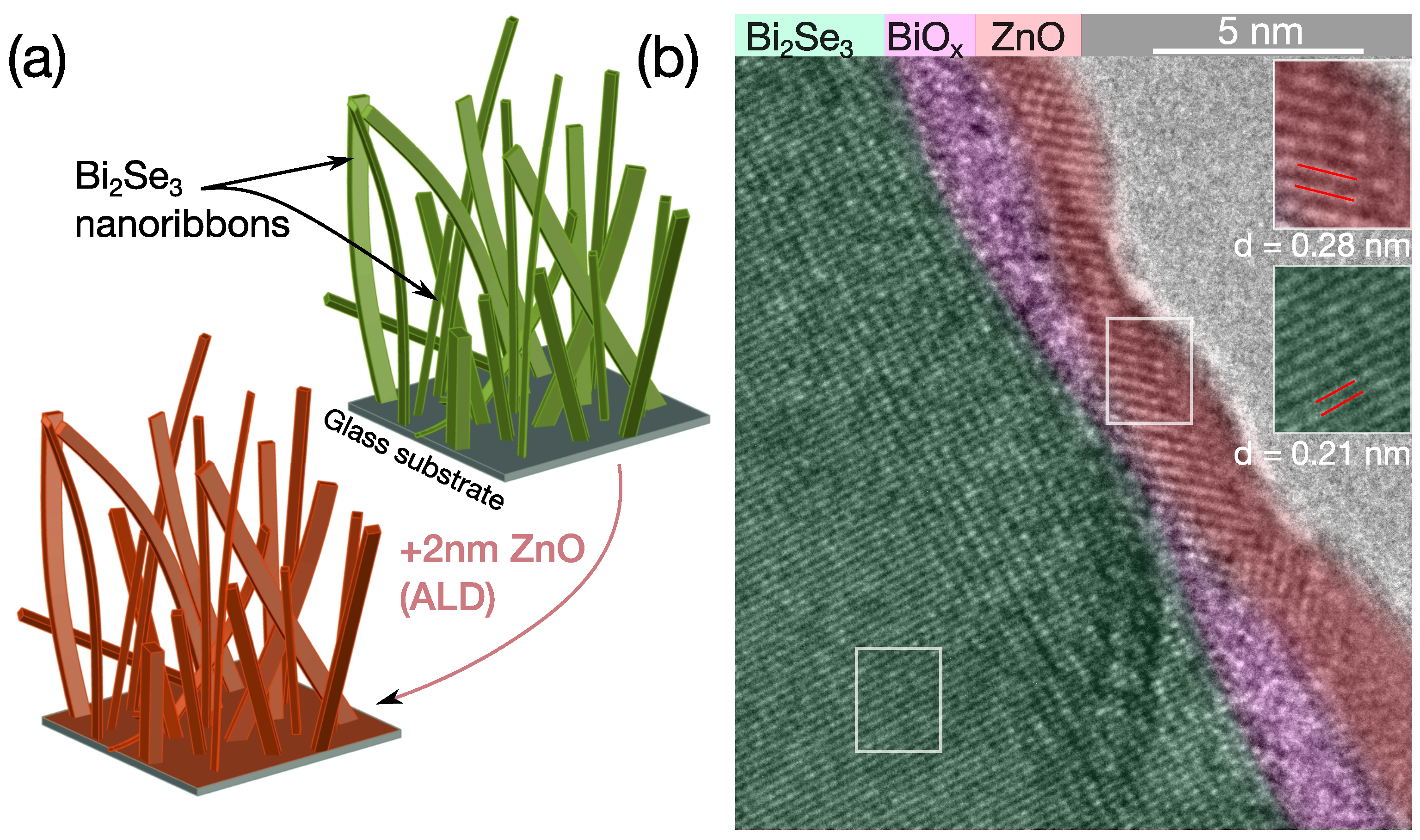
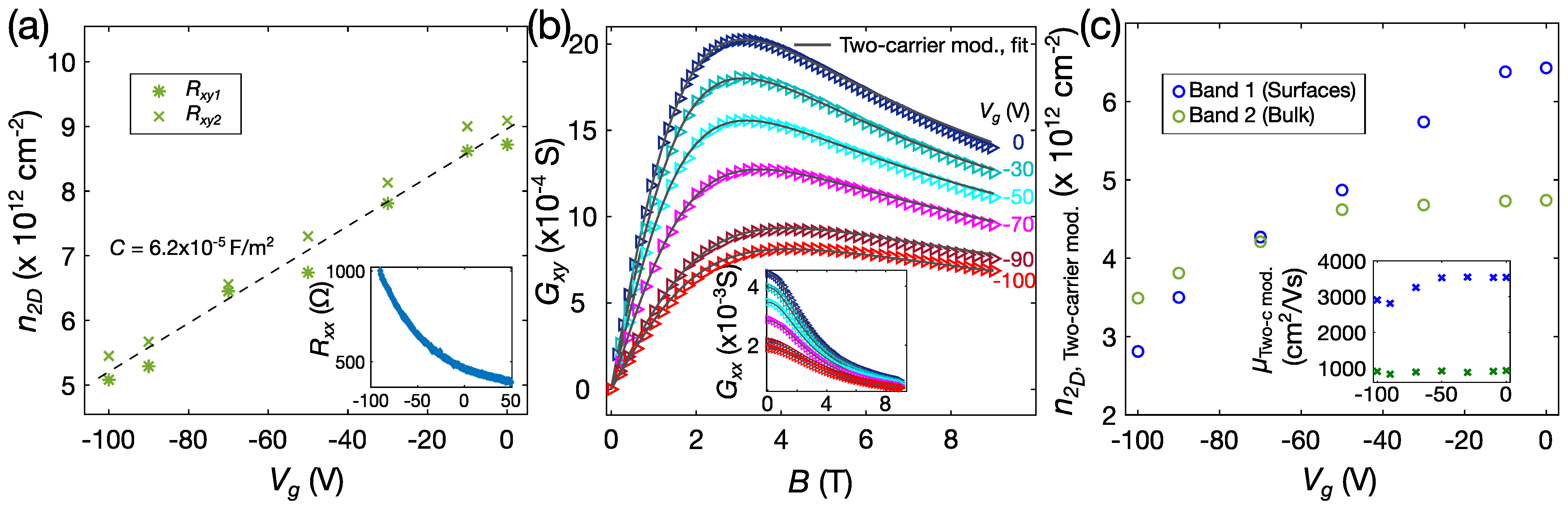
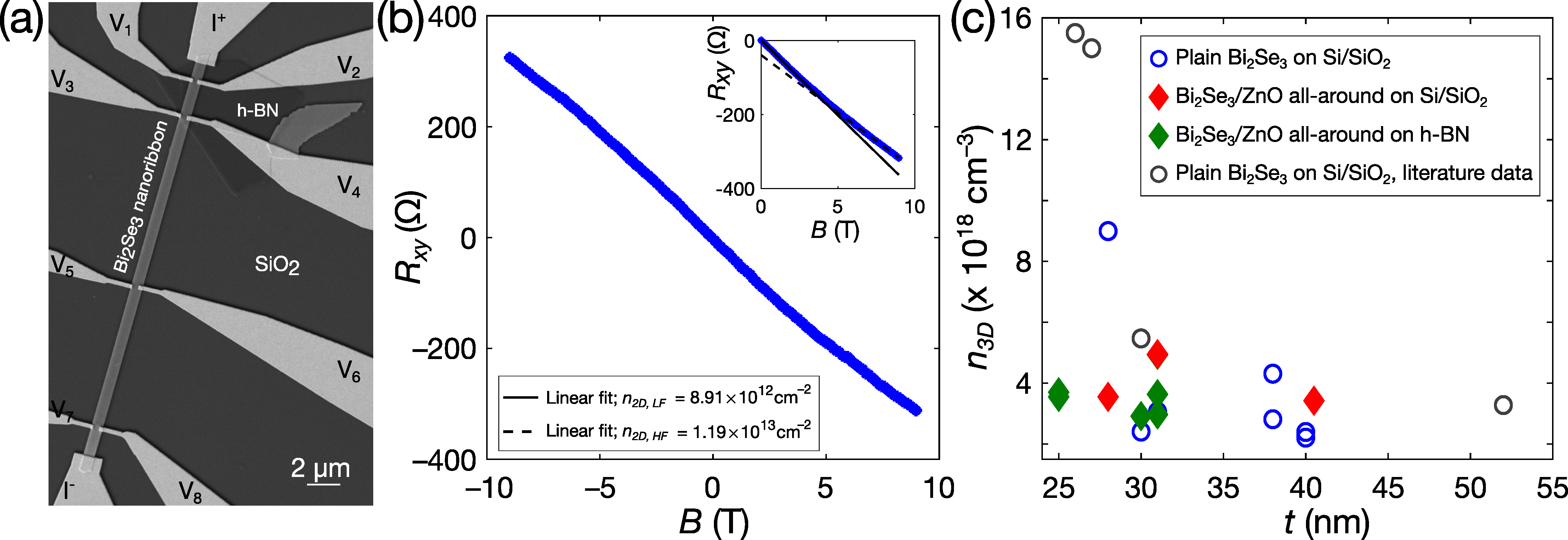
Figure 1. (a) Schematic representation of catalyst-free PVD-synthesized free-standing Bi2Se3 nanoribbons on glass substrate; (b) false-colored HR-TEM image of a Bi2Se3 nanoribbon after encapsulation with a thin layer of ZnO.
Nanomaterials 12 00768 g001
Figure 2. (a) SEM image of a Bi2Se3 nanoribbon Hall-bar device; (b) Hall resistance R x y B for the ZnO/Bi2Se3 nanoribbon device A3t (see Table S1), measured at back-gate voltage V g = 0 V. The inset shows anti-symmetrized R x y B data with linear fit in the 0–2.5 T range (black solid curve), and in the 7–9 T range (black dashed curve); (c) Hall carrier density of Bi2Se3 and ZnO/Bi2Se3 nanoribbons, plotted versus the nanoribbon thickness. In the case of the ZnO/Bi2Se3 nanoribbons, total thickness t is reduced by 4 nm, accounting for the two ~2 nm thick ZnO layers. Gray data points correspond to the data from [14]; here, the carrier density is calculated from the same magnetic field range (0–2.5 T).
Nanomaterials 12 00768 g002
Figure 3. (a) Charge carrier density n 2 D ( = n 3 D t ) as a function of the back-gate voltage V g . Here, n 2 D is calculated from the anti-symmetrized R x y B data in the 0–2.5 T range. R x y 1 and R x y 2 represent the Hall resistances measured using two different pairs of transversal electrodes, on the same nanoribbon. Black dashed line is the linear fit, and the capacitance estimated from the slope is 6.2 × 10⁻⁵ F/m2. In the inset—longitudinal resistance R x x as a function of the V g ; (b) conductance tensor element G x y B at different applied V g , fitted with the two-carrier model, inset shows fitted G x x B curves; (c) from the two-carrier model extracted parameters of the two bands: carrier densities n 1 ; n 2 , and mobilities μ 1 ; μ 2 (in the inset) versus the back-gate voltage. All the data shown correspond to the ZnO/Bi2Se3 nanoribbon A3t.
Nanomaterials 12 00768 g003
Table 1. Summary of the carrier densities (cm−2) and mobilities (cm2/Vs) extracted from the two-band analysis and from the SdH oscillations for ZnO-encapsulated Bi2Se3 nanoribbons on h-BN and SiO2 substrates, and comparison with the literature data (refs. [14,15,17]).
Surfaces (Band 1)Bulk (Band 2)Top Surface *Bulk *
ZnO/Bi2Se3 NR on h-BN:tNR, nm n 1 μ 1 n 2 μ 2 n 2 D ,   S d H n 3 D ,   S d H
A3t296.43 × 101235404.74 × 1012/1.64 × 1018930
A1b357.18 × 101247005.31 × 1012/1.52 × 101820522.40 × 10121.44 × 1018
D3b346.24 × 101248004.99 × 1012/1.46 × 10181350
Bi2Se3 NR on SiO2,
sample E5 [14]
3015.0 × 1012 ** 2.40 × 10¹²
Bi2Se3 NR on SiO2,
sample BR3-10R2 [14]
63- 2.50 × 10121.70 × 1018
Bi2Se3 NR on SiO2,
sample E [17]
7913.0 × 1012 * 2.90 × 10126.60 × 1017
Bi2Se3 NR on STO,
sample B51-10 [15]
95.55 × 10¹² **1232
* Extracted from analysis of the SdH oscillations. ** These values account only carrier density of the nanoribbon bottom surface/substrate interface.
Publisher’s Note: MDPI stays neutral with regard to jurisdictional claims in published maps and institutional affiliations.

