Large-Sized Nanocrystalline Ultrathin β-Ga2O3 Membranes Fabricated by Surface Charge Lithography

 , , , , , ,
  , and
, and
Abstract
1. Introduction
2. Materials and Methods
2.1. Fabrication of β-Ga2O3 Membranes
2.2. EM Analysis
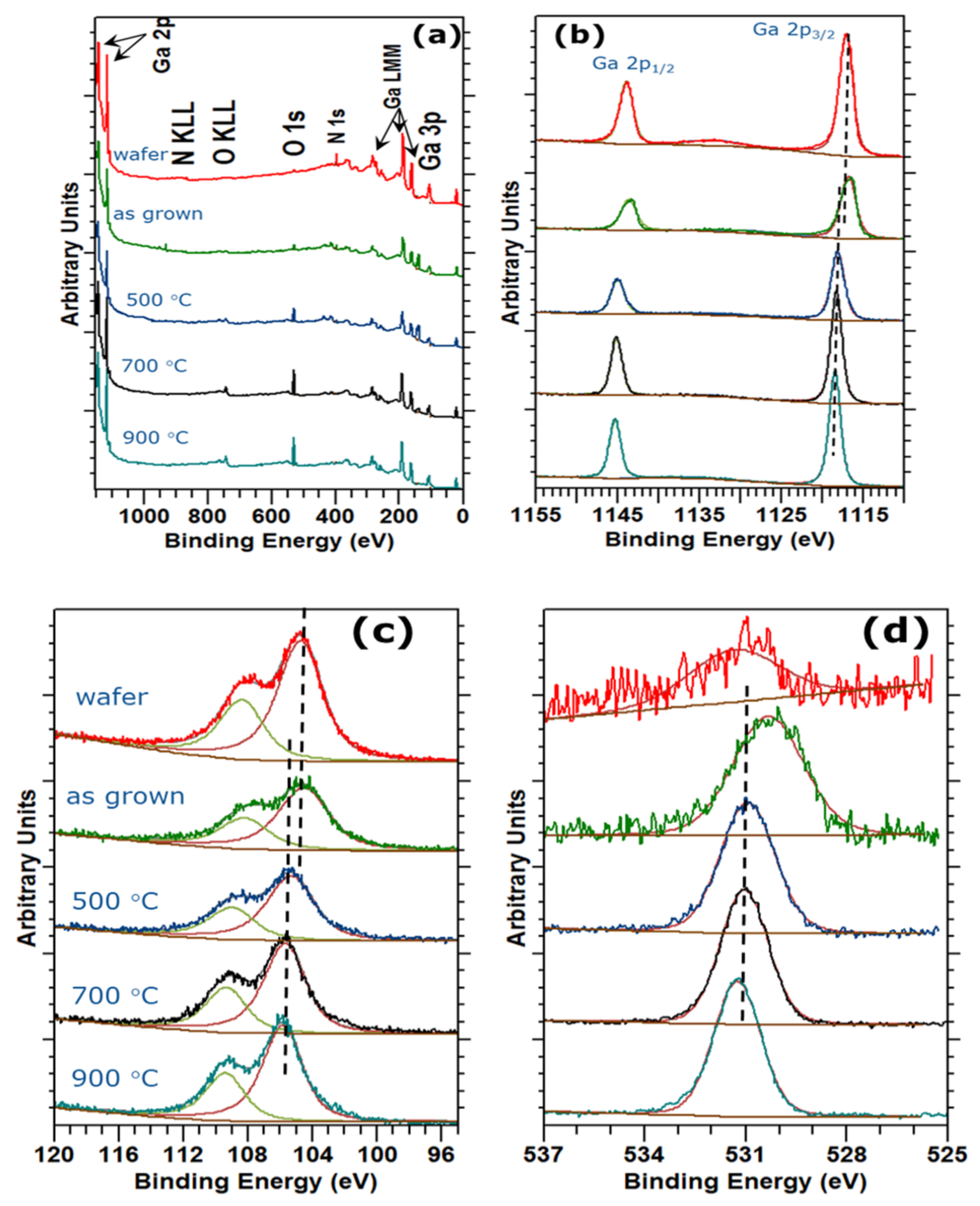
2.3. XPS Analysis
2.4. AFM
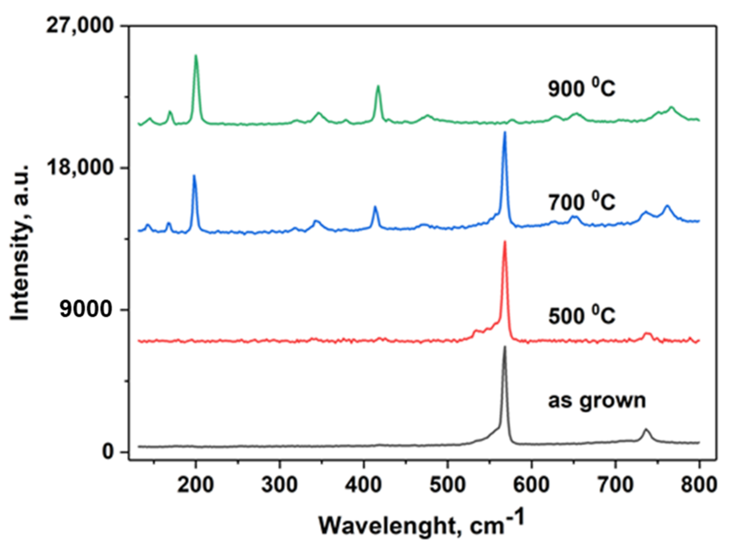
2.5. Raman
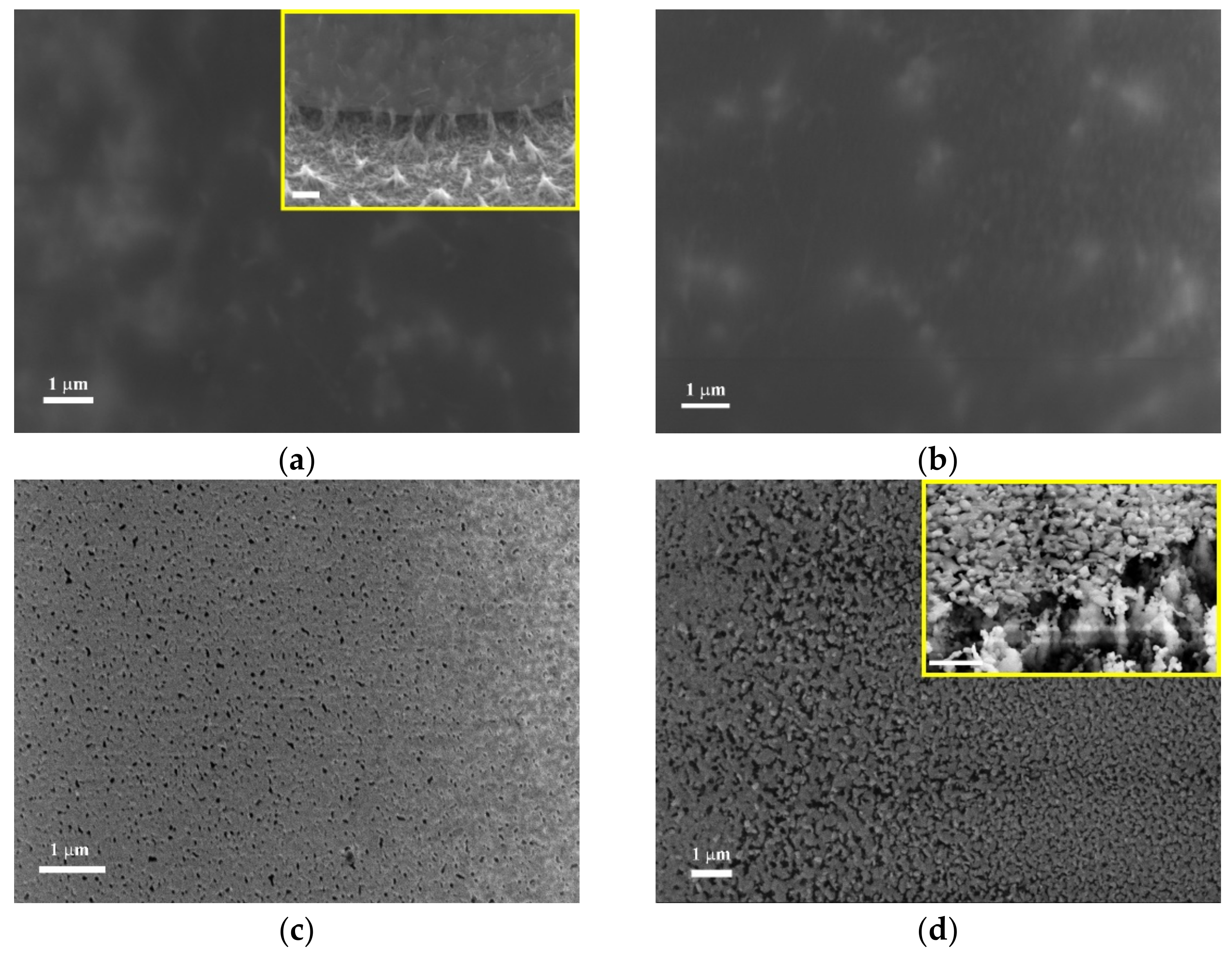
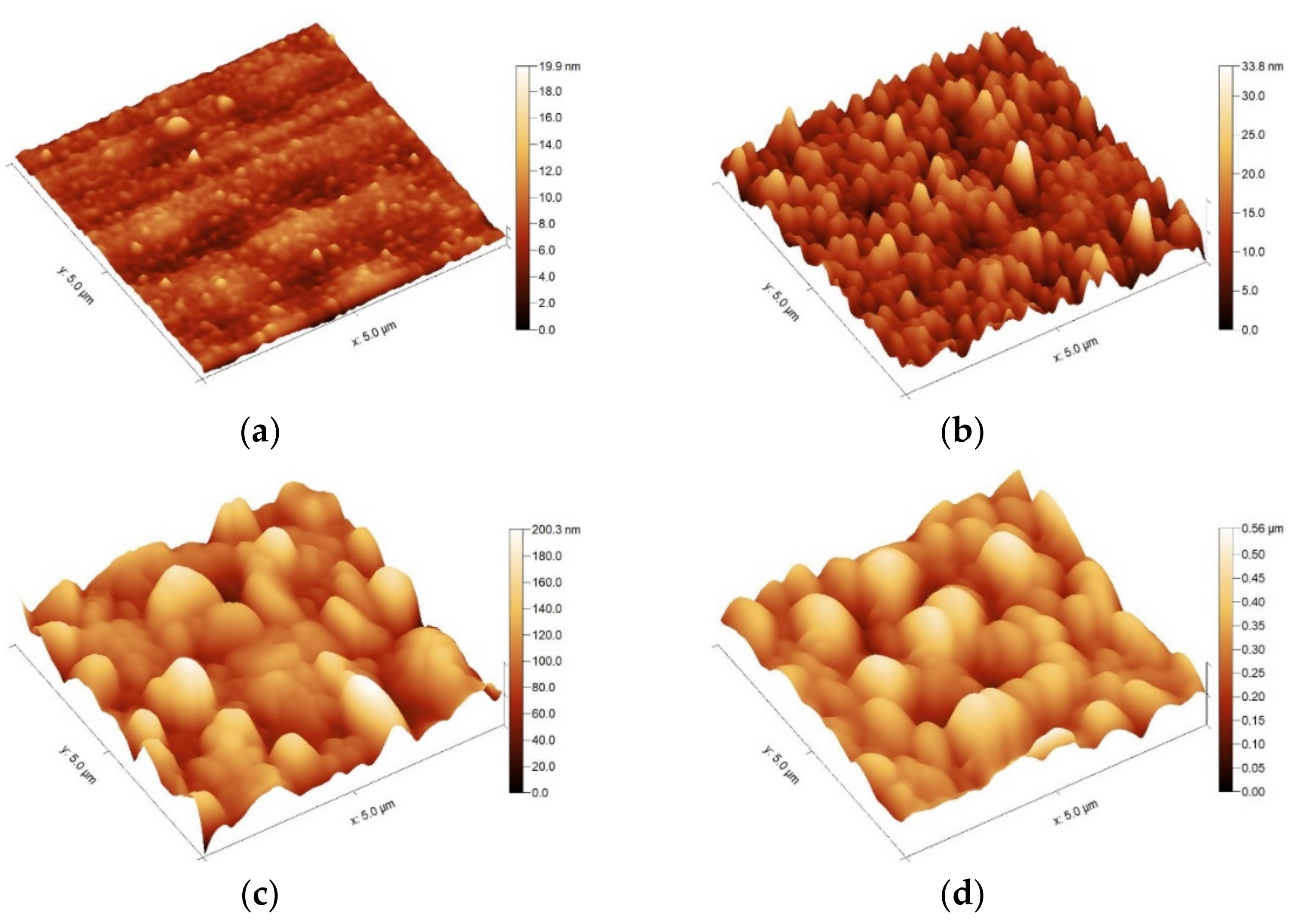
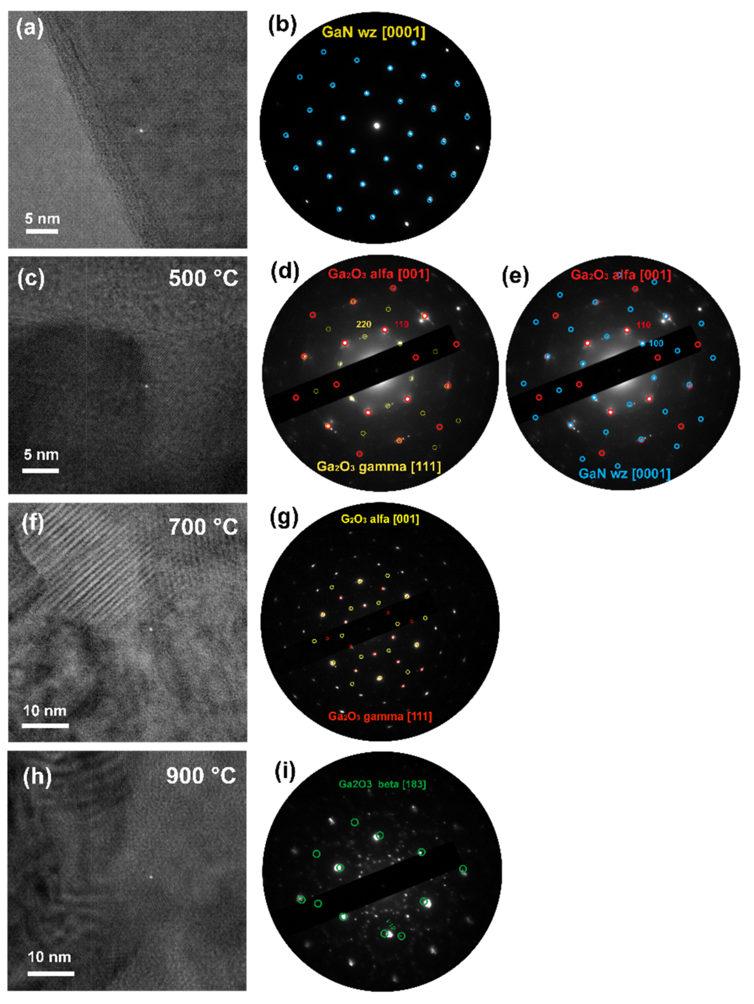
3. Results and Discussion
4. Conclusions
Author Contributions
Funding
Institutional Review Board Statement
Informed Consent Statement
Data Availability Statement
Conflicts of Interest
References
- Lv, Y.; Wang, Y.; Fu, X.; Dun, S.; Sun, Z.; Liu, H.; Zhou, X.; Song, X.; Dang, K.; Liang, S.; et al. Demonstration of β-Ga2O3 Junction Barrier Schottky Diodes with a Baliga’s Figure of Merit of 0.85 GW/cm2 or a 5A/700 V Handling Capabilities. IEEE Trans. Power Electron. 2021, 36, 6179–6182. [Google Scholar] [CrossRef]
- Higashiwaki, M.; Sasaki, K.; Kuramata, A.; Masui, T.; Yamakoshi, S. Gallium oxide (Ga2O3) metal-semiconductor field-effect transistors on single-crystal β-Ga2O3 (010) substrates. Appl. Phys. Lett. 2012, 100, 13504. [Google Scholar] [CrossRef]
- Higashiwaki, M.; Sasaki, K.; Kuramata, A.; Masui, T.; Yamakoshi, S. Development of gallium oxide power devices. Phys. Status Solidi (A) 2014, 211, 21–26. [Google Scholar] [CrossRef]
- Tadjer, M.J.; Mahadik, N.A.; Wheeler, V.D.; Glaser, E.R.; Ruppalt, L.; Koehler, A.D.; Hobart, K.D.; Eddy, C.R.; Kub, F.J. Editors’ Choice Communication—A (001) β-Ga2O3 MOSFET with +2.9 V Threshold Voltage and HfO2 Gate Dielectric. ECS J. Solid State Sci. Technol. 2016, 5, P468–P470. [Google Scholar] [CrossRef]
- Braniste, T.; Dragoman, M.; Zhukov, S.; Aldrigo, M.; Ciobanu, V.; Iordanescu, S.; Alyabyeva, L.; Fumagalli, F.; Ceccone, G.; Raevschi, S.; et al. Aero-Ga2O3 nanomaterial electromagnetically transparent from microwaves to terahertz for internet of things applications. Nanomaterials 2020, 10, 47. [Google Scholar] [CrossRef]
- He, H.; Blanco, M.A.; Pandey, R. Electronic and thermodynamic properties of β-Ga2O3. Appl. Phys. Lett. 2006, 88, 261904. [Google Scholar] [CrossRef]
- Mastro, M.A.; Kuramata, A.; Calkins, J.; Kim, J.; Ren, F.; Pearton, S.J. Perspective—Opportunities and Future Directions for Ga2O3. ECS J. Solid State Sci. Technol. 2017, 6, P356–P359. [Google Scholar] [CrossRef]
- Higashiwaki, M.; Murakami, H.; Kumagai, Y.; Kuramata, A. Current status of Ga2O3 power devices. Jpn. J. Appl. Phys. 2016, 55, 1202A1. [Google Scholar] [CrossRef]
- Roy, R.; Hill, V.G.; Osborn, E.F. Polymorphism of Ga2O3 and the System Ga2O3−H2O. J. Am. Chem. Soc. 1952, 74, 719–722. [Google Scholar] [CrossRef]
- Hoshikawa, K.; Ohba, E.; Kobayashi, T.; Yanagisawa, J.; Miyagawa, C.; Nakamura, Y. Growth of β-Ga2O3 single crystals using vertical Bridgman method in ambient air. J. Cryst. Growth 2016, 447, 36–41. [Google Scholar] [CrossRef]
- Wolten, G.M.; Chase, A.B. Determination of the point group of β-Ga2O3 from morphology and physical properties. J. Solid State Chem. 1976, 16, 377–383. [Google Scholar] [CrossRef]
- Tomm, Y.; Ko, J.M.; Yoshikawa, A.; Fukuda, T. Floating zone growth of β-Ga2O3: A new window material for optoelectronic device applications. Sol. Energy Mater. Sol. Cells 2001, 66, 369–374. [Google Scholar] [CrossRef]
- Kuramata, A.; Koshi, K.; Watanabe, S.; Yamaoka, Y.; Masui, T.; Yamakoshi, S. High-quality β-Ga2O3 single crystals grown by edge-defined film-fed growth. Jpn. J. Appl. Phys. 2016, 55, 1202A2. [Google Scholar] [CrossRef]
- Galazka, Z.; Irmscher, K.; Uecker, R.; Bertram, R.; Pietsch, M.; Kwasniewski, A.; Naumann, M.; Schulz, T.; Schewski, R.; Klimm, D.; et al. On the bulk β-Ga2O3 single crystals grown by the Czochralski method. J. Cryst. Growth 2014, 404, 184–191. [Google Scholar] [CrossRef]
- Oshima, T.; Okuno, T.; Fujita, S. Ga2O3 Thin Film Growth on c-Plane Sapphire Substrates by Molecular Beam Epitaxy for Deep-Ultraviolet Photodetectors. Jpn. J. Appl. Phys. 2007, 46, 7217–7220. [Google Scholar] [CrossRef]
- Feng, Z.; Karim, M.R.; Zhao, H. Low pressure chemical vapor deposition of β-Ga2O3 thin films: Dependence on growth parameters. APL Mater. 2018, 7, 22514. [Google Scholar] [CrossRef]
- Cheng, Z.; Wheeler, V.D.; Bai, T.; Shi, J.; Tadjer, M.J.; Feygelson, T.; Hobart, K.D.; Goorsky, M.S.; Graham, S. Integration of polycrystalline Ga2O3 on diamond for thermal management. Appl. Phys. Lett. 2020, 116, 62105. [Google Scholar] [CrossRef]
- Murakami, H.; Nomura, K.; Goto, K.; Sasaki, K.; Kawara, K.; Thieu, Q.T.; Togashi, R.; Kumagai, Y.; Higashiwaki, M.; Kuramata, A.; et al. Homoepitaxial growth of β-Ga2O3 layers by halide vapor phase epitaxy. Appl. Phys. Express 2014, 8, 15503. [Google Scholar] [CrossRef]
- Chen, Y.; Liang, H.; Xia, X.; Tao, P.; Shen, R.; Liu, Y.; Feng, Y.; Zheng, Y.; Li, X.; Du, G. The lattice distortion of β-Ga2O3 film grown on c-plane sapphire. J. Mater. Sci. Mater. Electron. 2015, 26, 3231–3235. [Google Scholar] [CrossRef]
- Cheng, Z.; Mu, F.; You, T.; Xu, W.; Shi, J.; Liao, M.E.; Wang, Y.; Huynh, K.; Suga, T.; Goorsky, M.S.; et al. Thermal Transport across Ion-Cut Monocrystalline β-Ga2O3 Thin Films and Bonded β-Ga2O3–SiC Interfaces. ACS Appl. Mater. Interfaces 2020, 12, 44943–44951. [Google Scholar] [CrossRef]
- Kim, J.; Mastro, M.A.; Tadjer, M.J.; Kim, J. Quasi-Two-Dimensional h-BN/β-Ga2O3 Heterostructure Metal–Insulator–Semiconductor Field-Effect Transistor. ACS Appl. Mater. Interfaces 2017, 9, 21322–21327. [Google Scholar] [CrossRef] [PubMed]
- Ding, S.; Zhang, L.; Li, Y.; Xiu, X.; Xie, Z.; Tao, T.; Liu, B.; Chen, P.; Zhang, R.; Zheng, Y. A Selective Etching Route for Large-Scale Fabrication of β-Ga2O3 Micro-/Nanotube Arrays. Nanomaterials 2021, 11, 327. [Google Scholar] [CrossRef] [PubMed]
- Zhang, X.; Wang, L.; Wang, X.; Chen, Y.; Shao, Q.; Wu, G.; Wang, X.; Lin, T.; Shen, H.; Wang, J.; et al. High-performance β-Ga2O3 thickness dependent solar blind photodetector. Opt. Express 2020, 28, 4169–4177. [Google Scholar] [CrossRef] [PubMed]
- Kim, S.J.; Park, S.Y.; Kim, K.H.; Kim, S.W.; Kim, T.G. Ga2O3:ITO transparent conducting electrodes for near-ultraviolet light-emitting diodes. IEEE Electron Device Lett. 2014, 35, 232–234. [Google Scholar] [CrossRef]
- Jeon, H.M.; Leedy, K.D.; Look, D.C.; Chang, C.S.; Muller, D.A.; Badescu, S.C.; Vasilyev, V.; Brown, J.L.; Green, A.J.; Chabak, K.D. Homoepitaxial β-Ga2O3 transparent conducting oxide with conductivity σ = 2323 S cm−1. APL Mater. 2021, 9, 101105. [Google Scholar] [CrossRef]
- Zhao, J.; Huang, X.; Yin, Y.; Liao, Y.; Mo, H.; Qian, Q.; Guo, Y.; Chen, X.; Zhang, Z.; Hua, M. Two-Dimensional Gallium Oxide Monolayer for Gas-Sensing Application. J. Phys. Chem. Lett. 2021, 12, 5813–5820. [Google Scholar] [CrossRef]
- Konishi, K.; Goto, K.; Murakami, H.; Kumagai, Y.; Kuramata, A.; Yamakoshi, S.; Higashiwaki, M. 1-kV vertical Ga2O3 field-plated Schottky barrier diodes. Appl. Phys. Lett. 2017, 110, 103506. [Google Scholar] [CrossRef]
- Hwang, W.S.; Verma, A.; Peelaers, H.; Protasenko, V.; Rouvimov, S.; (Grace) Xing, H.; Seabaugh, A.; Haensch, W.; Van de Walle, C.; Galazka, Z.; et al. High-voltage field effect transistors with wide-bandgap β-Ga2O3 nanomembranes. Appl. Phys. Lett. 2014, 104, 203111. [Google Scholar] [CrossRef]
- Li, X.; Zhen, X.; Meng, S.; Xian, J.; Shao, Y.; Fu, X.; Li, D. Structuring β-Ga2O3 Photonic Crystal Photocatalyst for Efficient Degradation of Organic Pollutants. Environ. Sci. Technol. 2013, 47, 9911–9917. [Google Scholar] [CrossRef]
- Zhou, J.; Chen, H.; Fu, H.; Fu, K.; Deng, X.; Huang, X.; Yang, T.-H.; Montes, J.A.; Yang, C.; Qi, X.; et al. Demonstration of low loss β-Ga2O3 optical waveguides in the UV–NIR spectra. Appl. Phys. Lett. 2019, 115, 251108. [Google Scholar] [CrossRef]
- Chen, H.; Fu, H.; Huang, X.; Montes, J.A.; Yang, T.-H.; Baranowski, I.; Zhao, Y. Characterizations of the nonlinear optical properties for (010) and (-201) beta-phase gallium oxide. Opt. Express 2018, 26, 3938–3946. [Google Scholar] [CrossRef]
- Volciuc, O.; Sergentu, V.; Tiginyanu, I.; Schowalter, M.; Ursaki, V.; Rosenauer, A.; Hommel, D.; Gutowski, J. Photonic Crystal Structures Based on GaN Ultrathin Membranes. J. Nanoelectron. Optoelectron. 2014, 9, 271–275. [Google Scholar] [CrossRef]
- Tiginyanu, I.M.; Popa, V.; Volciuc, O. Surface-charge lithography for GaN microstructuring based on photoelectrochemical etching techniques. Appl. Phys. Lett. 2005, 86, 174102. [Google Scholar] [CrossRef]
- Dragoman, M.; Tiginyanu, I.; Dragoman, D.; Braniste, T.; Ciobanu, V. Memristive GaN ultrathin suspended membrane array. Nanotechnology 2016, 27, 295204. [Google Scholar] [CrossRef] [PubMed][Green Version]
- Tiginyanu, I.M.; Popa, V.; Stevens-Kalceff, M.A.; Gerthsen, D.; Brenner, P.; Pavlidis, D. Design and maskless fabrication of ultrathin suspended membranes of GaN. Phys. Status Solidi—Rapid Res. Lett. 2012, 6, 148–150. [Google Scholar] [CrossRef]
- Yamada, T.; Ito, J.; Asahara, R.; Watanabe, K.; Nozaki, M.; Nakazawa, S.; Anda, Y.; Ishida, M.; Ueda, T.; Yoshigoe, A.; et al. Comprehensive study on initial thermal oxidation of GaN(0001) surface and subsequent oxide growth in dry oxygen ambient. J. Appl. Phys. 2017, 121, 35303. [Google Scholar] [CrossRef]
- Feng, Z.C.; Wang, W.; Chua, S.J.; Zhang, P.X.; Williams, K.P.J.; Pitt, G.D. Raman scattering properties of GaN thin films grown on sapphire under visible and ultraviolet excitation. J. Raman Spectrosc. 2001, 32, 840–846. [Google Scholar] [CrossRef]
- Kranert, C.; Sturm, C.; Schmidt-Grund, R.; Grundmann, M. Raman tensor elements of β-Ga2O3. Sci. Rep. 2016, 6, 35964. [Google Scholar] [CrossRef] [PubMed]
- Lai, Y.H.; Yeh, C.T.; Hwang, J.M.; Hwang, H.L.; Chen, C.T.; Hung, W.H. Sputtering and Etching of GaN Surfaces. J. Phys. Chem. B 2001, 105, 10029–10036. [Google Scholar] [CrossRef]
- Huang, R.; Li, F.; Liu, T.; Zhao, Y.; Zhu, Y.; Shen, Y.; Lu, X.; Huang, Z.; Liu, J.; Zhang, L.; et al. Ion Sputter Induced Interfacial Reaction in Prototypical Metal-GaN System. Sci. Rep. 2018, 8, 8521. [Google Scholar] [CrossRef]
- Zhong, Y.; Su, S.; Zhou, Y.; Gao, H.; Chen, X.; He, J.; Zhan, X.; Sun, Q.; Yang, H. Effect of Thermal Cleaning Prior to p-GaN Gate Regrowth for Normally Off High-Electron-Mobility Transistors. ACS Appl. Mater. Interfaces 2019, 11, 21982–21987. [Google Scholar] [CrossRef]
- Vauche, L.; Chanuel, A.; Martinez, E.; Roure, M.-C.; Le Royer, C.; Bécu, S.; Gwoziecki, R.; Plissonnier, M. Study of an Al2O3/GaN Interface for Normally Off MOS-Channel High-Electron-Mobility Transistors Using XPS Characterization: The Impact of Wet Surface Treatment on Threshold Voltage VTH. ACS Appl. Electron. Mater. 2021, 3, 1170–1177. [Google Scholar] [CrossRef]
- Kang, H.S.; Siva Pratap Reddy, M.; Kim, D.S.; Kim, K.W.; Ha, J.B.; Lee, Y.S.; Choi, H.C.; Lee, J.H. Effect of oxygen species on the positive flat-band voltage shift in Al2O3/GaN metal–insulator–semiconductor capacitors with post-deposition annealing. J. Phys. D Appl. Phys. 2013, 46, 155101. [Google Scholar] [CrossRef]
- Gangopadhyay, S.; Schmidt, T.; Kruse, C.; Figge, S.; Hommel, D.; Falta, J. Surface oxidation of GaN(0001): Nitrogen plasma-assisted cleaning for ultrahigh vacuum applications. J. Vac. Sci. Technol. A 2014, 32, 51401. [Google Scholar] [CrossRef]
- Ilhom, S.; Mohammad, A.; Shukla, D.; Grasso, J.; Willis, B.G.; Okyay, A.K.; Biyikli, N. Low-Temperature As-Grown Crystalline β-Ga2O3 Films via Plasma-Enhanced Atomic Layer Deposition. ACS Appl. Mater. Interfaces 2021, 13, 8538–8551. [Google Scholar] [CrossRef] [PubMed]


| Sample | Ga 3d Peak Position (eV) |
|---|---|
| Wafer | 19.46 |
| As grown | 19.26 |
| 500 °C | 19.97 |
| 700 °C | 20.28 |
| 900 °C | 20.45 |
Publisher’s Note: MDPI stays neutral with regard to jurisdictional claims in published maps and institutional affiliations. |
© 2022 by the authors. Licensee MDPI, Basel, Switzerland. This article is an open access article distributed under the terms and conditions of the Creative Commons Attribution (CC BY) license (https://creativecommons.org/licenses/by/4.0/).
Share and Cite
Ciobanu, V.; Ceccone, G.; Jin, I.; Braniste, T.; Ye, F.; Fumagalli, F.; Colpo, P.; Dutta, J.; Linnros, J.; Tiginyanu, I. Large-Sized Nanocrystalline Ultrathin β-Ga2O3 Membranes Fabricated by Surface Charge Lithography. Nanomaterials 2022, 12, 689. https://doi.org/10.3390/nano12040689
Ciobanu V, Ceccone G, Jin I, Braniste T, Ye F, Fumagalli F, Colpo P, Dutta J, Linnros J, Tiginyanu I. Large-Sized Nanocrystalline Ultrathin β-Ga2O3 Membranes Fabricated by Surface Charge Lithography. Nanomaterials. 2022; 12(4):689. https://doi.org/10.3390/nano12040689
Chicago/Turabian StyleCiobanu, Vladimir, Giacomo Ceccone, Irina Jin, Tudor Braniste, Fei Ye, Francesco Fumagalli, Pascal Colpo, Joydeep Dutta, Jan Linnros, and Ion Tiginyanu. 2022. "Large-Sized Nanocrystalline Ultrathin β-Ga2O3 Membranes Fabricated by Surface Charge Lithography" Nanomaterials 12, no. 4: 689. https://doi.org/10.3390/nano12040689
APA StyleCiobanu, V., Ceccone, G., Jin, I., Braniste, T., Ye, F., Fumagalli, F., Colpo, P., Dutta, J., Linnros, J., & Tiginyanu, I. (2022). Large-Sized Nanocrystalline Ultrathin β-Ga2O3 Membranes Fabricated by Surface Charge Lithography. Nanomaterials, 12(4), 689. https://doi.org/10.3390/nano12040689