
Reduced Electron Temperature in Silicon Multi-Quantum-Dot Single-Electron Tunneling Devices


Abstract
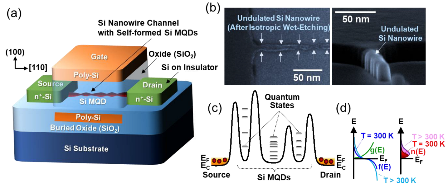
:1. Introduction
2. Experimental Section
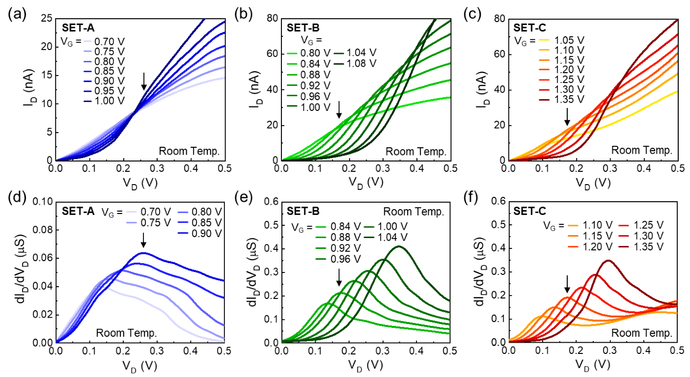
3. Results and Discussion
4. Summary and Conclusions
Supplementary Materials
Author Contributions
Funding
Institutional Review Board Statement
Informed Consent Statement
Data Availability Statement
Conflicts of Interest
References
- Knobel, R.G.; Cleland, A.N. Nanometre-scale displacement sensing using a single electron transistor. Nature 2003, 424, 291–293. [Google Scholar] [CrossRef] [PubMed]
- Knobel, R.; Cleland, A.N. Piezoelectric displacement sensing with a single-electron transistor. Appl. Phys. Lett. 2002, 81, 2258–2260. [Google Scholar] [CrossRef]
- Mahboob, I.; Nishiguchi, K.; Fujiwara, A.; Yamaguchi, H. Room temperature piezoelectric displacement detection via a silicon field effect transistor. Appl. Phys. Lett. 2009, 95, 233102. [Google Scholar] [CrossRef]
- van der Wiel, W.G.; De Franceschi, S.; Elzerman, J.M.; Fujisawa, T.; Tarucha, S.; Kouwenhoven, L.P. Electron transport through double quantum dots. Rev. Mod. Phys. 2002, 75, 1–22. [Google Scholar] [CrossRef] [Green Version]
- Oda, S.; Ferry, D.K. Silicon Nanoelectronics; Taylor & Francis: New York, NY, USA, 2006. [Google Scholar]
- Jing, Y.; Huang, S.; Wu, J.; Meng, M.; Li, X.; Zhou, Y.; Peng, H.; Xu, H. A Single-Electron Transistor Made of a 3D Topological Insulator Nanoplate. Adv. Mater. 2019, 31, 1903686. [Google Scholar] [CrossRef] [Green Version]
- Lee, S.; Lee, Y.; Song, E.B.; Wang, K.L.; Hiramoto, T. Gate-Tunable Selective Operation of Single Electron/Hole Transistor Modes in a Silicon Single Quantum Dot at Room Temperature. Appl. Phys. Lett. 2013, 102, 083504. [Google Scholar] [CrossRef]
- Lee, S.; Lee, Y.; Song, E.B.; Hiramoto, T. Modulation of Peak-to-Valley Current Ratio of Coulomb Blockade Oscillations in Si Single Hole Transistors. Appl. Phys. Lett. 2013, 103, 103502. [Google Scholar] [CrossRef]
- Lee, Y.; Lee, J.W.; Lee, S.; Hiramoto, T.; Wang, K.L. Reconfigurable Multivalue Logic Functions of a Silicon Ellipsoidal Quantum-Dot Transistor Operating at Room Temperature. ACS Nano 2021, 15, 18483–18493. [Google Scholar] [CrossRef]
- Lee, S.; Lee, Y.; Song, E.B.; Hiramoto, T. Observation of Single Electron Transport via Multiple Quantum States of a Silicon Quantum Dot at Room Temperature. Nano Lett. 2014, 14, 71–77. [Google Scholar] [CrossRef]
- Lee, S.; Lee, Y.; Song, E.B.; Hiramoto, T. The Characteristic of Elongated Coulomb-Blockade Regions in a Si Quantum-Dot Device Coupled via Asymmetric Tunnel Barriers. J. Appl. Phys. 2013, 114, 164513. [Google Scholar] [CrossRef]
- Lee, Y.; Lee, S.; Hiramoto, T. Transport Behaviors and Mechanisms in Cuspidal Blockade Region for Silicon Single-Hole Transistor. Curr. Appl. Phys. 2014, 14, 428–432. [Google Scholar] [CrossRef]
- Lee, S.; Miyaji, K.; Kobayashi, M.; Hiramoto, T. Extremely High Flexibilities of Coulomb Blockade and Negative Differential Conductance Oscillations in Room-Temperature-Operating Silicon Single Hole Transistor. Appl. Phys. Lett. 2008, 92, 073502. [Google Scholar] [CrossRef]
- Lee, Y.; Lee, S.; Im, H.; Hiramoto, T. Multiple Logic Functions from Extended Blockade Region in a Silicon Quantum-Dot Transistor. J. Appl. Phys. 2015, 117, 064501. [Google Scholar] [CrossRef]
- Lee, S.; Hiramoto, T. Strong Dependence of Tunneling Transport Properties on Overdriving Voltage for Room-Temperature-Operating Single Electron/Hole Transistors Formed with Ultranarrow [100] Silicon Nanowire Channel. Appl. Phys. Lett. 2008, 93, 043508. [Google Scholar] [CrossRef]
- Eenink, H.G.J.; Petit, L.; Lawrie, W.I.L.; Clarke, J.S.; Vandersypen, L.M.K.; Veldhorst, M. Tunable Coupling and Isolation of Single Electrons in Silicon Metal-Oxide-Semiconductor Quantum Dots. Nano Lett. 2019, 19, 8653–8657. [Google Scholar] [CrossRef] [Green Version]
- Yuan, M.; Yang, Z.; Savage, D.E.; Lagally, M.G.; Eriksson, M.A.; Rimberg, A.J. Charge sensing in a Si/SiGe quantum dot with a radio frequency superconducting single-electron transistor. Appl. Phys. Lett. 2012, 101, 142103. [Google Scholar] [CrossRef]
- Stuyck, N.D.; Li, R.; Kubicek, S.; Mohiyaddin, F.A.; Jussot, J.; Chan, B.T.; Simion, G.; Govoreanu, B.; Heyns, M.; Radu, I. An Integrated Silicon MOS Single-Electron Transistor Charge Sensor for Spin-Based Quantum Information Processing. IEEE Electron. Device Lett. 2020, 41, 1253–1256. [Google Scholar] [CrossRef]
- Chanrion, E.; Niegemann, D.J.; Bertrand, B.; Spence, C.; Jadot, B.; Li, J.; Mortemousque, P.-A.; Hutin, L.; Maurand, R.; Jehl, X.; et al. Charge Detection in an Array of CMOS Quantum Dots. Phys. Rev. Appl. 2020, 14, 024066. [Google Scholar] [CrossRef]
- Hensgens, T.; Fujita, T.; Janssen, L.; Li, X.; Van Diepen, C.J.; Reichl, C.; Wegscheider, W.; Das Sarma, S.; Vandersypen, L.M.K. Quantum simulation of a Fermi–Hubbard model using a semiconductor quantum dot array. Nature 2017, 548, 70–73. [Google Scholar] [CrossRef]
- Reed, M.D.; Maune, B.M.; Andrews, R.W.; Borselli, M.G.; Eng, K.; Jura, M.P.; Kiselev, A.A.; Ladd, T.D.; Merkel, S.T.; Milosavljevic, I.; et al. Reduced Sensitivity to Charge Noise in Semiconductor Spin Qubits via Symmetric Operation. Phys. Rev. Lett. 2016, 116, 110402. [Google Scholar] [CrossRef]
- Martins, F.; Malinowski, F.K.; Nissen, P.D.; Barnes, E.; Fallahi, S.; Gardner, G.C.; Manfra, M.J.; Marcus, C.M.; Kuemmeth, F. Noise Suppression Using Symmetric Exchange Gates in Spin Qubits. Phys. Rev. Lett. 2016, 116, 116801. [Google Scholar] [CrossRef] [PubMed] [Green Version]
- Nakajima, A. Application of Single-Electron Transistor to Biomolecule and Ion Sensors. Appl. Sci. 2016, 6, 94. [Google Scholar] [CrossRef]
- Brun-Picard, J.; Djordjevic, S.; Leprat, D.; Schopfer, F.; Poirier, W. Practical Quantum Realization of the Ampere from the Elementary Charge. Phys. Rev. X 2016, 6, 041051. [Google Scholar] [CrossRef] [Green Version]
- Chen, I.H.; Lai, W.T.; Li, P.W. Realization of solid-state nanothermometer using Ge quantum-dot single-hole transistor in few-hole regime. Appl. Phys. Lett. 2014, 104, 243506. [Google Scholar] [CrossRef]
- Meschke, M.; Kemppinen, A.; Pekola, J.P. Accurate Coulomb blockade thermometry up to 60 kelvin. Philos. Trans. A Math. Phys. Eng. Sci. 2016, 374, 20150052. [Google Scholar] [CrossRef] [Green Version]
- Ghirri, A.; Cornia, S.; Affronte, M. Microwave Photon Detectors Based on Semiconducting Double Quantum Dots. Sensors 2020, 20, 4010. [Google Scholar] [CrossRef]
- Nishiguchi, K.; Ono, Y.; Fujiwara, A.; Yamaguchi, H.; Inokawa, H.; Takahashi, Y. Infrared detection with silicon nano-field-effect transistors. Appl. Phys. Lett. 2007, 90, 223108. [Google Scholar] [CrossRef]
- Nishiguchi, K.; Clement, N.; Yamaguchi, T.; Fujiwara, A. Si nanowire ion-sensitive field-effect transistors with a shared floating gate. Appl. Phys. Lett. 2009, 94, 163106. [Google Scholar] [CrossRef]
- Clément, N.; Nishiguchi, K.; Dufreche, J.F.; Guerin, D.; Fujiwara, A.; Vuillaume, D. A silicon nanowire ion-sensitive field-effect transistor with elementary charge sensitivity. Appl. Phys. Lett. 2011, 98, 014104. [Google Scholar] [CrossRef] [Green Version]
- Schupp, F.J. Single-electron devices in silicon. Mater. Sci. Technol. 2017, 33, 944–962. [Google Scholar] [CrossRef]
- Averin, D.V.; Odintsov, A.A.; Vyshenskii, S.V. Ultimate accuracy of single-electron dc current standards. J. Appl. Phys. 1993, 73, 1297–1308. [Google Scholar] [CrossRef]
- Ohkura, K.; Kitade, T.; Nakajima, A. Cotunneling Current in Si Single-Electron Transistor Based on Multiple Islands. Appl. Phys. Lett. 2006, 89, 183520. [Google Scholar] [CrossRef] [Green Version]
- Kobayashi, M.; Hiramoto, T. Experimental Study on Quantum Confinement Effects in Silicon Nanowire Metal-Oxide-Semiconductor Field-Effect Transistors and Single-Electron Transistors. J. Appl. Phys. 2008, 103, 053709. [Google Scholar] [CrossRef]
- Kobayashi, M.; Hiramoto, T. Large Coulomb-Blockade Oscillations and Negative Differential Conductance in Silicon Single-Electron Transistors with [100]- and [110]-Directed Channels at Room Temperature. Jpn. J. Appl. Phys. 2007, 46, 24–27. [Google Scholar] [CrossRef]
- Neophytou, N.; Paul, A.; Lundstrom, M.S.; Klimeck, G. Bandstructure Effects in Silicon Nanowire Electron Transport. IEEE Trans. Electron Dev. 2008, 55, 1286–1297. [Google Scholar] [CrossRef] [Green Version]
- Yi, K.S.; Trivedi, K.; Floresca, H.C.; Yuk, H.; Hu, W.; Kim, M.J. Room-Temperature Quantum Confinement Effects in Transport Properties of Ultrathin Si Nanowire Field-Effect Transistors. Nano Lett. 2011, 11, 5465–5470. [Google Scholar] [CrossRef]
- Kobayashi, M.; Saitoh, M.; Hiramoto, T. Large Temperature Dependence of Coulomb Blockade Oscillations in Room-Temperature-Operating Silicon Single-Hole Transistor. Jpn. J. Appl. Phys. 2006, 45, 6157–6161. [Google Scholar] [CrossRef]
- Basu, T.S.; Wakayama, Y.; Hayakawa, R. Theoretical Insight into Quantum Transport Via Molecular Dots in a Vertical Tunnel Transistor. ACS Appl. Electron. Mater. 2021, 3, 973–978. [Google Scholar] [CrossRef]
- Gotszalk, T.; Jóźwiak, G.; Radojewski, J.; Fröhlich, T.; Füssl, R.; Manske, E.; Holz, M.; Ivanov, T.; Ahmad, A.; Rangelow, I.W. Tip-Based Nano-Manufacturing and -Metrology. J. Vac. Sci. Technol. B 2019, 37, 030803. [Google Scholar] [CrossRef]
- Liu, Q.; Zhao, J.; Guo, J.; Wu, R.; Liu, W.; Chen, Y.; Du, G.; Duan, H. Sub-5 nm Lithography with Single GeV Heavy Ions Using Inorganic Resist. Nano Lett. 2021, 21, 2390–2396. [Google Scholar] [CrossRef]
- Li, L.; Liu, X.; Pal, S.; Wang, S.; Ober, C.K.; Giannelis, E.P. Extreme Ultraviolet Resist Materials for Sub-7 nm Patterning. Chem. Soc. Rev. 2017, 46, 4855–4866. [Google Scholar] [CrossRef]
- Hiramoto, T. Five Nanometre CMOS Technology. Nat. Electron. 2019, 2, 557–558. [Google Scholar] [CrossRef]
- Kwak, J.; Mishra, A.K.; Lee, J.; Lee, K.S.; Choi, C.; Maiti, S.; Kim, M.; Kim, J.K. Fabrication of Sub-3 nm Feature Size Based on Block Copolymer Self-Assembly for Next-Generation Nanolithography. Macromolecules 2017, 50, 6813–6818. [Google Scholar] [CrossRef]
- Averin, D.V.; Nazarov, Y.V. Virtual Electron Diffusion During Quantum Tunneling of the Electric Charge. Phys. Rev. Lett. 1990, 65, 2446–2449. [Google Scholar] [CrossRef] [PubMed]
- Takahashi, Y.; Horiguchi, S.; Fujiwara, A.; Murase, K. Co-Tunneling Current in Very Small Si Single-Electron Transistors. Physica B 1996, 227, 105–108. [Google Scholar] [CrossRef]
- De Franceschi, S.; Sasaki, S.; Elzerman, J.M.; van der Wiel, W.G.; Tarucha, S.; Kouwenhoven, L.P. Electron Cotunneling in a Semiconductor Quantum Dot. Phys. Rev. Lett. 2001, 86, 878–881. [Google Scholar] [CrossRef] [Green Version]


| Number of QD | Device Type | Si Nanowire Direction | Teff (K) | Eexc (meV) | Ref. |
|---|---|---|---|---|---|
| Single | Si SHT | [100] | 1260 | 82.7 | [15] |
| Si SHT | [100] | 870 | 49.1 | [15] | |
| Si SHT | [100] | 415 | 9.9 | [15] | |
| Si SET | [110] | 312 | 1.0 | [10] | |
| Si SET | [100] | 338 | 3.3 | [9] | |
| Double | Si SET (A) | [110] | 376 | 6.5 | This Work |
| Si SET (B) | [110] | 349 | 4.2 | ||
| Si SET (S1) | [110] | 384 | 7.2 | ||
| Si SET (S2) | [110] | 389 | 7.7 | ||
| Si SET (S3) | [110] | 397 | 8.4 | ||
| Triple | Si SET (C) | [110] | 335 | 3.0 | |
| Si SET (S4) | [110] | 342 | 3.4 |
Publisher’s Note: MDPI stays neutral with regard to jurisdictional claims in published maps and institutional affiliations. |
© 2022 by the authors. Licensee MDPI, Basel, Switzerland. This article is an open access article distributed under the terms and conditions of the Creative Commons Attribution (CC BY) license (https://creativecommons.org/licenses/by/4.0/).
Share and Cite
Lee, Y.; Lee, S.H.; Son, H.S.; Lee, S. Reduced Electron Temperature in Silicon Multi-Quantum-Dot Single-Electron Tunneling Devices. Nanomaterials 2022, 12, 603. https://doi.org/10.3390/nano12040603
Lee Y, Lee SH, Son HS, Lee S. Reduced Electron Temperature in Silicon Multi-Quantum-Dot Single-Electron Tunneling Devices. Nanomaterials. 2022; 12(4):603. https://doi.org/10.3390/nano12040603
Chicago/Turabian StyleLee, Youngmin, So Hyun Lee, Hyo Seok Son, and Sejoon Lee. 2022. "Reduced Electron Temperature in Silicon Multi-Quantum-Dot Single-Electron Tunneling Devices" Nanomaterials 12, no. 4: 603. https://doi.org/10.3390/nano12040603
APA StyleLee, Y., Lee, S. H., Son, H. S., & Lee, S. (2022). Reduced Electron Temperature in Silicon Multi-Quantum-Dot Single-Electron Tunneling Devices. Nanomaterials, 12(4), 603. https://doi.org/10.3390/nano12040603