Article

Field Emission of Multi-Walled Carbon Nanotubes from Pt-Assisted Chemical Vapor Deposition

Wenzhou Key Lab of Micro-nano Optoelectronic Devices, Wenzhou University, Wenzhou 325035, China
*
Author to whom correspondence should be addressed.
Nanomaterials 2022, 12(3), 575; https://doi.org/10.3390/nano12030575
Submission received: 31 December 2021 / Revised: 27 January 2022 / Accepted: 2 February 2022 / Published: 8 February 2022
(This article belongs to the Special Issue The Research Related to Nanomaterial Cold Cathode)

Abstract

:
Multi-walled carbon nanotubes (MWNTs) were grown directly on a metal substrate with the assistance of Pt using a chemical vapor deposition method. In addition, the growth mechanism of Pt-assisted catalytic CNT was discussed. MWNTs were characterized by SEM, TEM, AFM, Raman, and EDS, and the field emission (FE) properties were investigated, comparing with the direct grown MWNTs. The results showed that CNTs could not been synthesized by Pt particles alone under the experimental condition, but Pt may accelerate the decomposition of the carbon source gas, i.e., assisting MWNT growth with other catalysts. The Pt-assisted MWNTs were longer with larger diameters of around 80 nm and possessed better structural qualities with very few catalyst particles inside. Improved field emission properties were demonstrated for the Pt-assisted MWNTs with lower turn-on fields (for 0.01 mA·cm−2 current density) of 2.0 V·μm−1 and threshold field (for 10 mA·cm−2 current density) of 3.5 V·μm−1, as well as better stability under a long-term test of 80 h (started at 3.0 mA for the Pt-assisted emitter and 3.25 mA for the direct grown emitter). This work demonstrated a promising approach to develop high performance CNT field emitters for device applications.

1. Introduction

Due to unique structural, chemical, and physical properties, carbon nanotubes (CNTs) have been applied and investigated in various areas [1,2,3,4]. With the advantages of large aspect ratio, high electrical conductivity, and good thermal stability, CNTs present excellent field emission properties for different types of vacuum electronic devices [5,6,7]. However, there are still many issues for practical applications, including emission uniformity and emission stabilities in high pressure ambiences. The improvement of CNT film production with emission enhancement is crucial to promote the device’s developments.
Among various carbon nanotube synthesis techniques, chemical vapor deposition (CVD) is widely employed for simple processing, in situ growth on various substrates, and low cost. In most CVD synthesis, carbon nanotubes are grown from the catalyst films, e.g., Fe, Co, and Ni, and deposited on the substrates [8,9]. Bronikowski investigated the effects of multiple factors on the synthesis of carbon nanotube bundle arrays with Fe catalyst on Si substrates [10]. Terrado et al. prepared uniform multi-walled carbon nanotubes by spraying precipitated Co catalyst particles on quartz substrates and discussed the effects of catalyst pretreatment and growth temperature on CNT diameters [11]. The direct growth of CNTs on metallic substrates containing catalyst elements exhibited significant advantages, including the enhancement of adhesion and reduction in contact resistance between CNTs and the substrates, resulting in improvements in field emission properties. Direct CNT growth demonstrates great potentials for field emission device applications [5,12,13,14]. Beyond typical single element catalyst (e.g., Fe, Co, Ni, etc.), multi-element catalysts, such as Ni alloys, have been found to present prominent catalytic effects for CNT synthesis [5,15,16,17]. CNT growth mechanisms from multi-catalyst systems are mostly ambiguous. Kiang et al. suggested that synergistic effects of large bi-metal catalyst, such as Co and Bi, result in the expansion of CNT diameters [18]. Teng et al. synthesized CNTs from the Co-Cr-Pt-O catalytic system and attributed simply the synergistic effect for growth [19]. Researchers also reported that tungsten, molybdenum, and sulfur could be used as the auxiliary catalyst to improve catalyst activity and increase the yield of carbon nanotubes [20,21]. Bimetallic catalyst combination (Ni + Co) resulted in 10–100 times higher growth rate than those of nickel or cobalt alone in the arc discharge synthesis of single-wall CNTs [22]. Sridhar et al. synthesized MWNTs on Inconel alloy substrates by water-assisted chemical vapor deposition with good field emission properties from high local field enhancement factors [23].
In carbon nanotube synthesis, Pt is rarely used as the catalyst. Iijima et al. successfully prepared single-walled carbon nanotubes (SWNTs) by ethanol with Pt as the catalyst, where SWNTs with diameters smaller than 1 nm were synthesized under low pressure (1 × 10⁻⁴ Pa) and low temperature (400 °C), showing that Pt has high catalytic activity [24,25]. Synthesis of MWNT films on the catalytic substrates, mainly transition metal-based alloy materials, showed advantages of process simplicity and substrate flexibility [26,27,28]. In this work, we proposed a novel direct MWNT growth method on Pt coated Ni alloy substrates. Structural and field emission properties are characterized by comparing with the MWNT emitters by the direct growth method. Pt-assisted MWNT emitters exhibited better structural quality with significant improvements on field emission performances.

2. Materials and Methods

Ni alloy substrates (Ni:Cr:Fe:Co = 57.5:15.5:6:1.5) of 0.2 mm in thickness were employed for the investigation. For direct growth, the substrate was anodized in the oxalic acid solution and ultrasonically cleaned with ethanol and ultrapurified water. For Pt-assisted growth, the substrate was coated with Pt by magnetron sputtering under a power of 40 W. Pt film was 35 nm thick measure by the film thickness detector of the sputtering system (VTC-16-SM, Kejing, Hefei, China). The sputtering chamber was evacuated to about 2 Pa at first, and then Ar gas was introduced to increase the pressure to 9 Pa before sputtering the high-purity Pt target (purity: 99.99%). After sputtering, the substrate was placed in the CVD system, which was evacuated to about 4 Pa by a mechanical pump and heated to 500 °C with purging Ar gas as a carrier gas. After reaching 750 °C, C2H2 was introduced to increase the pressure to 1.0 × 10³ Pa for 10 min to grow the MWNTs. In the contrast, the MWNT emitters on the alloy substrate was also directly synthesized by the above CVD process without Pt deposition. Structural and field emission properties were comparatively investigated.
The structural and elemental properties of MWNTs were characterized by scanning electron microscopy (SEM, JSM-7100F, JEOL, Tokyo, Japan), transmission electron microscopy (TEM, JEM-2100, JEOL, Tokyo, Japan), Atomic Force Microscope (AFM, Nanowizard 3, JPK, Berlin, Germany), and energy-dispersive X-ray analysis (EDS). The contact resistance of the MWNT film relative to the substrate was tested by the dual electrodynamic four-probe method by the Probe Station (PEH-4, EverBeing, Taiwan, China) and Keithley 2440 multimeter (Tektronix, State of Oregon, USA). Field emission performances were investigated in a high vacuum turbo system with the base pressure in 10−7 Pa level after baking the system at 250℃ for 12 h. In the diode field emission setup, the CNT emission film area was 12 mm2, and the cathode and anode were spaced 300 μm apart. The Keithley 248 power supply was employed to provide the emission potential.

3. Results

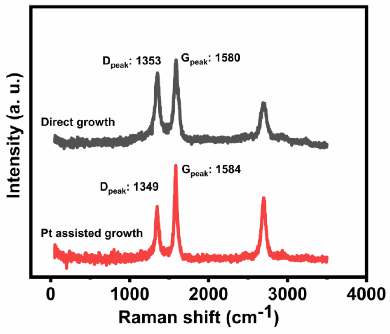
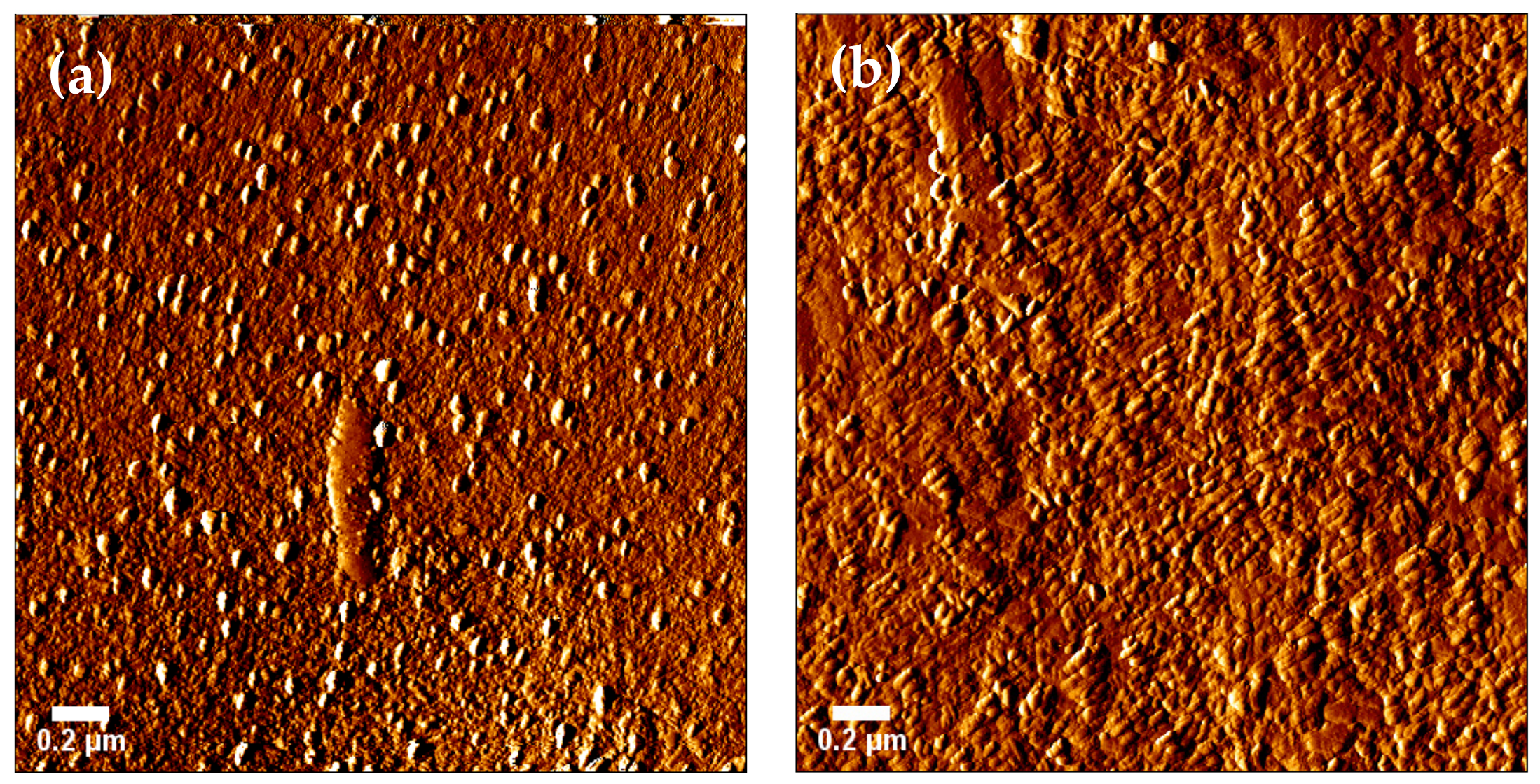
3.1. Structural Characterization of Carbon Nanotubes

Both Pt-assisted and the direct grown MWNTs were randomly oriented and exhibit good structural homogeneities, as shown in Figure 1. However, the addition of Pt elements affected CNT growth significantly. The Pt-assisted MWNTs could be 10 μm long with larger tube diameters in the 70~90 nm range, while the direct grown MWNTs were shorter and denser with lengths of ~1 μm and diameters in the 50~70 nm range (Figure 2). Random orientation and good homogeneity are favorable for reducing emission hot spots and the edge effect from local excessive Joule heating under high emission to burn the long CNT away [29,30]. According to high magnification SEM (Figure 1c,d) and TEM (Figure 1e,f) images, the Pt-assisted MWNTs show less amorphous carbon to outer walls with smoother surfaces. There were fewer catalyst particles inside Pt-assisted MWNTs, which would help to improve electronic and thermal conductivities. In contrast, more catalyst particles were detected along direct growth MWNTs, especially inside the caps.
What is rarer is that there still exist catalyst particles inside Pt-assisted MWNTs. Thus, EDS mapping was applied to identify catalyst components. As shown in Figure 3, beside the carbon element, the catalyst particle inside the tube top consisted of Fe, Co, and Ni elements, which were from the metal substrate, but the Pt element was not identified, with the exception of scattered noise signals.
Raman characteristic performances were investigated for two types of MWNTs, as shown in Figure 4. The D peak at 1360 cm−1 and G peak at 1584 cm−1 correspond to vibration modes of defect structures and crystal graphite, respectively. The D peak to G peak ratio is always used to evaluate CNT crystallinity, and the smaller the ID/IG, the better the structural quality. The ID/IG ratio of direct grown MWNTs was 0.73, which is better than MWNTs on the Inconel alloy substrate [23,31], while the ID/IG of Pt-assisted MWNTs could reach 0.56, indicating improvements on structural perfection.
The surface morphologies of two types of substrates before the growth were analyzed. Figure 5 shows AFM analysis of the substrates right before MWNT growth, i.e., after heating at 750 °C in Ar for 10 min. The catalyst particles of about 60 nm, which were in the same dimension of the MWNT diameters, are believed to serve as the growth catalysts, distributed uniformly on the substrate surface for direct growth (Figure 5a). For the Pt-coated substrate, the surface was in tight bonded form with narrow belt shape bulges (Figure 5b). The EDS result showed that the Pt element covered the entire substrate surface (Figure S1). For comparison, we failed to grow CNTs for either sputtering Pt films on Si substrates or depositing Pt films of more than 50 nm on alloy substrates, implying that the single Pt element could not catalyze the CNT synthesis alone based on our growth system. The contact resistance properties of the MWNT films relative to the substrates were characterized, as shown in Figure 6. The contact resistances from the slope are 4.68 Ω and 7.86 Ω, respectively, for Pt-assisted and direct growth MWNT films.
Based on the fact that Pt-assisted MWNTs exhibited very few catalyst particles inside, it may suggest a bottom growth mechanism. Pt film could play a crucial role in holding catalyst particles with the substrate, which is also supported by the fact that there were no Pt elements identified inside the tube from the element mapping above. The better electrical contact and field emission properties below also indicate stronger adhesions between Pt-assisted MWNTs relative to the substrate, supporting the bottom growth mechanism. According to cross-sectional SEM images of MWNTs, it was found that Pt-assisted MWNTs are about ten times longer compared with direct growth tubes under the same growth conditions. Therefore, Pt nanoparticles may accelerate the decompositions of acetylene molecules to grow longer and larger diameter MWNTs with better structural quality.

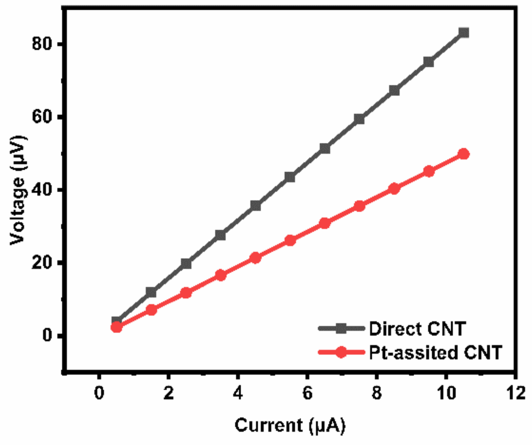
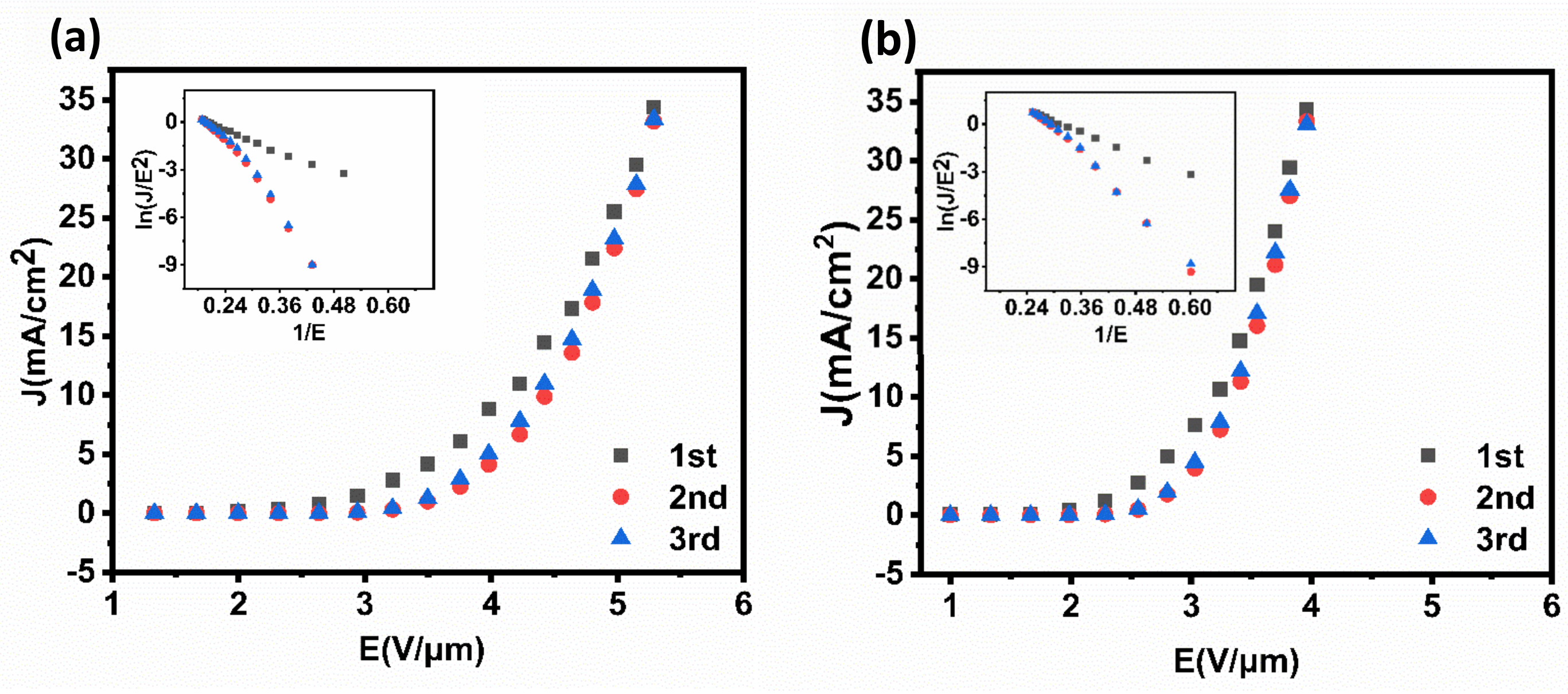
3.2. Field Emission Performance Test

Field emission performances of current density vs. electric field are illustrated in Figure 7 for both emitters (the field emission uniformity of the Pt-assisted MWNT film is shown in Figure S2), with insets of corresponding to Fowler–Nordheim (F-N) curves. Pt-assisted MWNTs showed better field emission characteristics than direct growth MWNT emitters. In three test cycles, the first cycle deviated from the second and third cycles, which are attributed to the desorptions of gas adsorbents [6,32]. Then, the second and third tests have good reproducibility. The turn-on field (for 0.01 mA·cm−2 current density) and the threshold field (for 10 mA·cm−2 current density) were 2.0 V·μm−1 and 3.5 V·μm−1, respectively, for the Pt-assisted emitter and improved significantly comparing with 2.7 V·μm−1 and 4.65 V·μm−1 for the direct grown emitter. According to the following F-N equation:
β = 6.83 × 10 3 × φ 3 2 / slope
where β is the field enhancement factor, φ is the work function (~4.8 eV for MWNT), and the slope is taken from the fitted F-N curve from the third and second test cycles. Thus, β values for the Pt-assisted and direct grown MWNTs are 2486 and 1942, respectively. It is clear that reductions of turn-on and threshold fields of the Pt-assisted MWNTs are attributed mainly to the increase in β.
The field emission stabilities of both types of emitters were tested in the high vacuum system, as shown in Figure 8. The emission currents started at 3.0 mA (25 mA·cm−2) for the Pt-assisted emitter and 3.25 mA (27 mA·cm−2) for the direct grown emitter. For the Pt-assisted emitter, the current fluctuated between 3.2 mA and 4.8 mA in the first 20 h and then stabilized at 3.6 mA for 80 h. For the direct grown emitter, the emission current dropped to 2.6 mA in 15 h, then reached stable emission around 2.8 mA with a fluctuation rate of ±1.25%. The initial current increase for the Pt-assisted emitters could be attributed to the CNT stretching effect by electrostatic force from the electric field [33,34], especially for curved long tubes, resulting in an increase in the field enhancement effect and a decrease in CNT–anode distance. It was suggested that the high emission current may cause uniform melting in the CNT-catalyst–substrate interface, which improves electrical conductivity and mechanical strength at the interface [20]. Such effects may be more obvious for the Pt-assisted emitters, which could have better adhesions with the substrate for the bottom growth model, helping the initial current increase. After such a stretching period, poorly bonded MWNTs may be pulled off from the substrate. Meanwhile, emission hot spots could be burned away by over current Joule heating, resulting in the current decay. After such aging process, emission reached quite stable levels with a fluctuation rate of less than 1%. While for the direct grown emitters, the tube was shorter; thus, the stretching effect was weak. Therefore, during the initial aging period, burning away hot spots and low crystallinity tubes may play key roles, resulting in emission decline.

4. Conclusions

MWNT field emitters were synthesized on a Pt-coated Ni alloy substrate by thermal CVD, and the structural and field emission properties were investigated in comparison with the direct grown MWNTs. The Pt-assisted MWNTs were longer with larger diameters of around 80 nm and possessed better structural qualities with very few catalyst particles inside. The Pt-assisted MWNTs exhibited improved field emission characteristics with the turn-on field of 2.0 V·μm−1 and the threshold field of 3.5 V·μm−1. MWNTs presented excellent emission stability under the current density of ~30 mA·cm−2 with a current fluctuation of less than 1%. This work presented a new approach to synthesize CNT field emitters for device applications.

Supplementary Materials

The following are available online at https://www.mdpi.com/article/10.3390/nano12030575/s1, Figure S1: EDS mapping of Pt coated substrate after heating, Figure S2: Field emission uniformity of Pt assisted MWNT film with emission area of 12 mm2.

Author Contributions

Data curation, H.T., W.H. and W.Z.; formal analysis, W.Q.; funding acquisition, C.D.; investigation, H.T. and R.L.; supervision, C.D.; writing—original draft, H.T.; writing—review and editing, C.D. All authors have read and agreed to the published version of the manuscript.

Funding

The authors gratefully acknowledge the financial support by National Natural Science Foundation of China (Grant No. 61620106006) and the Graduate Scientific Research Foundation of Wenzhou University.

Data Availability Statement

The data presented in this study are available on request from the corresponding author. The data are not publicly aviable due to privacy restrictions.

Conflicts of Interest

The authors declare no conflict of interest.

References

  1. Dai, H.; Xiao, D.; He, H.; Li, H.; Yuan, D.; Zhang, C. Synthesis and analytical applications of molecularly imprinted polymers on the surface of carbon nanotubes: A review. Microchim. Acta 2015, 182, 893–908. [Google Scholar]
  2. Ren, X.; Chen, C.; Nagatsu, M.; Wang, X. Carbon nanotubes as adsorbents in environmental pollution management: A review. Chem.Eng. J. 2011, 170, 395–410. [Google Scholar] [CrossRef]
  3. Liu, X.-M.; Huang, Z.D.; Oh, S.W.; Zhang, B.; Ma, P.-C.; Yuen, M.M.; Kim, J.-K. Carbon nanotube (CNT)-based composites as electrode material for rechargeable Li-ion batteries: A review. Compos. Sci. Technol. 2012, 72, 121–144. [Google Scholar] [CrossRef]
  4. Niu, L.; Luo, Y.L.; Li, Z. A highly selective chenical gassensor based on functionalization of multi-walled carbon nanotubes with poly (ethylene glycol). Sens. Actuat. B-Chem. 2007, 126, 361–367. [Google Scholar] [CrossRef]
  5. Dong, C.; Gupta, M.C. Influences of the surface reactions on thefield emission from multiwall carbon nanotubes. Appl. Phys. Lett. 2003, 83, 159–161. [Google Scholar] [CrossRef]
  6. Dong, C.; Luo, H.; Cai, J.; Wang, F.; Zhao, Y.; Li, D. Hydrogen sensing characteristics from carbon nanotube field emissions. Nanoscale 2016, 8, 5599–5604. [Google Scholar] [CrossRef]
  7. Hadsell, M.; Zhang, J.; Laganis, P.; Sprenger, F.; Shan, J.; Zhang, L.; Burk, L.; Yuan, H.; Chang, S.; Lu, J.; et al. A first generation compact microbeam radiation therapy system based on carbon nanotube X-ray technology. Appl. Phys. Lett. 2013, 103, 183505. [Google Scholar] [CrossRef] [Green Version]
  8. Moisala, A.; Nasibulin, A.G.; Kauppinen, E.I. The role of metal nanoparticles in the catalytic production of single-walled carbon nanotubes—A review. J. Phy. Condens. Mat. 2003, 15, S3011–S3035. [Google Scholar] [CrossRef]
  9. Dupuis, A.C. The catalyst in the CCVD of carbon nanotubes—A review. Prog. Mater. Sci. 2005, 50, 929–961. [Google Scholar] [CrossRef]
  10. Bronikowski, M.J. CVD growth of carbon nanotube bundle arrays. Carbon 2006, 44, 2822–2832. [Google Scholar] [CrossRef]
  11. Terrado, E.; Redrado, M.; Mun, E.; Maser, W.K.; Benito, A.M.; Martínez, M.T. Carbon nanotube growth on cobalt-sprayed substrates by thermal CVD. Mater. Sci. Eng. C. 2006, 26, 1185–1188. [Google Scholar] [CrossRef]
  12. Zhang, J.; Li, D.; Zhao, Y.; Cheng, Y.; Dong, C. Wide-range Vacuum Measurements from MWNT Field Emitters Grown Directly on Stainless Steel Substrates. Nanoscale Res. Lett. 2016, 11, 2–7. [Google Scholar] [CrossRef] [Green Version]
  13. Li, D.; Wang, Y.; Cheng, Y.; Feng, Y.; Zhao, L.; Zhang, H.; Sun, J.; Dong, C. An overview of ionization gauges with carbon nanotube cathodes. J. Phys. D Appl. Phys. 2015, 48, 473001. [Google Scholar] [CrossRef]
  14. Lee, Y.Z.; Burk, L.; Wang, K.H.; Cao, G.; Lu, J.; Zhou, O. Carbon Nanotube based X-ray Sources: Applications in Pre-Clinical and Medical Imaging. Nucl. Instrum. Meth. A. 2011, 648, S281–S283. [Google Scholar] [CrossRef] [Green Version]
  15. He, M.; Vasala, S.; Jiang, H.; Karppinen, M.; Kauppinen, E.I.; Niemelä, M.; Lehtonen, J. Growth and surface engineering of verticallyaligned low-wall-number carbon nanotubes. Carbon 2012, 50, 4750–4764. [Google Scholar] [CrossRef]
  16. Bayer, B.C.; Fouquet, M.; Blume, R.; Wirth, C.T.; Weatherup, R.S.; Ogata, K.; Knop-Gericke, A.; Schlögl, R.; Hofmann, S.; Robertson, J. Co-catalytic solid-state reduction applied to carbon nanotube growth. J. Phys. Chem. C. 2012, 116, 1107–1113. [Google Scholar] [CrossRef]
  17. Zhang, Q.; Zhao, M.; Huang, J.; Nie, J.; Wei, F. Mass prouction of aligned carbon nanotube arrays byfluidized bed catalytic chemical vapor deposition. Carbon 2010, 48, 1196–1209. [Google Scholar]
  18. Kiang, C.-H.; Goddard, W.; Beyers, R.; Salem, J.R.; Bethune, D.S. Catalytic Synthesis of Single-Layer Carbon Nanotubes with a Wide Range of Diameters. J. Phys. Chem. 1994, 98, 6612–6618. [Google Scholar] [CrossRef]
  19. Teng, I.; Huang, C.; Hsu, H.; Chung, I.; Jian, S.; Kherani, N.P.; Kuo, C.; Juang, J. On the use of new oxidized Co-Cr-Pt-O catalystsfor vertically-aligned few-walled carbon nanotube forest synthesis in electron cyclotron resonance chemical vapor deposition. Carbon 2014, 80, 808–822. [Google Scholar] [CrossRef]
  20. Wang, Z.; Gao, R.; Heer, W.; Poncharal, P. In situ imaging of field emission from individual carbon nanotubes and their structural damage. Appl. Phys. Lett. 2002, 80, 856–858. [Google Scholar] [CrossRef] [Green Version]
  21. Saito, R.; Fujita, M.; Dresselhaus, G.; Dresselhaus, M.S. Electronic structure of chiral graphene tubules. Appl. Phys. Lett. 1992, 60, 2204–2206. [Google Scholar] [CrossRef]
  22. Guo, T.; Nikolaev, P.; Thess, A.; Colbert, D.T.; Smalley, R.E. Catalytic growth of single-walled manotubes by laser vaporization. Chem. Phys. Lett. 1995, 243, 49–54. [Google Scholar] [CrossRef]
  23. Sridhar, S.V.; Ge, L.; Tiwary, C.S.; Hart, A.C.; Ozden, S.; Kalaga, K.; Lei, S.; Sinha, R.; Harsh, H.; Kordas, K.; et al. Enhanced field emission properties from CNT arrays synthesized on inconel superalloy. ACS Appl. Mater. Inter. 2014, 6, 1986–1991. [Google Scholar] [CrossRef]
  24. Maruyama, T.; Mizutani, Y.; Naritsuka, S.; Iijima, S. Single-Walled Carbon Nanotube Growth in High Vacuum Using Pt Catalyst in Alcohol Gas Source Method. Mater. Express. 2011, 1, 267–272. [Google Scholar] [CrossRef]
  25. Kondo, H.; Fukuoka, N.; Ghosh, R.; Naritsuka, S.; Maruyama, T.; Iijima, S. Low-Temperature Single-Walled Carbon Nanotube Growth from Pt Catalyst Using Alcohol Gas Source Method in High Vacuum. Jpn. J. Appl. Phys 2013, 52, 06GD02. [Google Scholar] [CrossRef]
  26. Neupane, S.; Lastres, M.; Chiarella, M.; Li, W. Synthesis and field emission properties of vertically aligned carbon nanotube arrays on copper. Carbon 2012, 50, 641–2650. [Google Scholar] [CrossRef]
  27. Kimura, H.; Zhao, B.; Futaba1, D.N.; Yamada, T.; Kurachi, H.; Uemura, K.; Hata, K. Field emission from laterally aligned carbon nanotube flower arrays for low turn-on field emission. APL Mater. 2013, 1, 032101. [Google Scholar] [CrossRef] [Green Version]
  28. Chen, G.; Neupane, S.; Li, W.; Chen, L.; Zhang, J. An increase in the field emission from vertically aligned multi-walled carbon nanotubes caused by NH3 plasma treatment. Carbon 2013, 52, 468–475. [Google Scholar] [CrossRef]
  29. Li, C.; Zhang, Y.; Mann, M.; Hasko, D.; Lei, W.; Wang, B.; Chu, D.; Pribat, D.; Amaratunga, G.A.J.; Milne, W.I. High emission current density, vertically aligned carbon nanotube mesh, field emitter array. Appl. Phys. Lett. 2010, 97, 113107. [Google Scholar] [CrossRef]
  30. Fujii, S.; Honda, S.-I.; Machida, H.; Kawai, H.; Ishida, K.; Katayama, M.; Furuta, H.; Hirao, T.; Oura, K. Efficient field emission from an individual aligned carbon nanotube bundle enhanced by edge effect. Appl. Phys. Lett. 2007, 90, 153108. [Google Scholar] [CrossRef]
  31. Atthipalli, G.; Wang, H.; Gray, J.L. Catalyst-assisted vertical growth of carbon nanotubes on Inconel coated commercial copper foil substrates versus sputtered copper films. Appl. Surf. Sci. 2013, 273, 515–519. [Google Scholar] [CrossRef]
  32. Zhao, Y.; Cai, J.; Luo, H.; Kang, S.; Qian, W.; Dong, C. Low pressure hydrogen sensing based on carbon nanotube field emission: Mechanism of atomic adsorption induced work function effects. Carbon 2017, 124, 669–674. [Google Scholar] [CrossRef]
  33. Verma, P.; Gautam, S.; Kumar, P.; Chaturvedi, P.; Rawat, J.S.; Pal, S.; Chaubey, R.; Harsh; Vyas, H.P.; Bhatnagar, P.K. Carbon nanotube tip melting with vacuum breakdown in cold cathode. J. Vac. Sci. Technol. B 2007, 25, 1584–1587. [Google Scholar] [CrossRef]
  34. Srividya, S.; Gautam, S.; Jha, P.; Kumar, P.; Kumar, A.; Ojha, U.S.; Rawat, J.S.B.S.; Pal, S.; Chaudhary, P.K.; Harsh, R.; et al. Decoration of cesium iodide nano particles on patterned carbon nanotube emitter arrays to improve their field emission. Appl. Surf. Sci. 2013, 15, 1497. [Google Scholar]
Figure 1. SEM and TEM images of two types of MWNTs. (a,c,e) direct growth. (b,d,f) Pt-assisted growth.
Nanomaterials 12 00575 g001
Figure 2. Diameter distributions of two types of MWNTs.
Nanomaterials 12 00575 g002
Figure 3. TEM-EDS mapping of Pt-assisted MWNT. (a) MWNT with catalyst particle inside the top. (bf) Element distributions for C, Fe, Ni, Co, and Pt.
Nanomaterials 12 00575 g003
Figure 4. Raman spectra of two types of MWNTs.
Nanomaterials 12 00575 g004
Figure 5. AFM images of the surface morphologies of two types of substrates before the growth. (a) Direct growth substrate. (b) Pt-coated substrate.
Nanomaterials 12 00575 g005
Figure 6. Contact resistance of two types of MWNTs.
Nanomaterials 12 00575 g006
Figure 7. Field emission J−E properties for two types of MWNT emitters with insets of F−N curves. (a) Direct growth MWNTs. (b) Pt-assisted growth.
Nanomaterials 12 00575 g007
Figure 8. Emission stability tests of two types MWNT emitters.
Nanomaterials 12 00575 g008
Publisher’s Note: MDPI stays neutral with regard to jurisdictional claims in published maps and institutional affiliations.

