
Optical Interconnects Finally Seeing the Light in Silicon Photonics: Past the Hype


Abstract
1. Introduction
1.1. Interconnect Bottleneck in Chip Multiprocessors (CMPs)
1.2. Optical Interconnects
1.3. Performance Requirements for Optical Interconnects
2. Components of an Optical Interconnect
2.1. Source
2.1.1. Off-Chip Sources
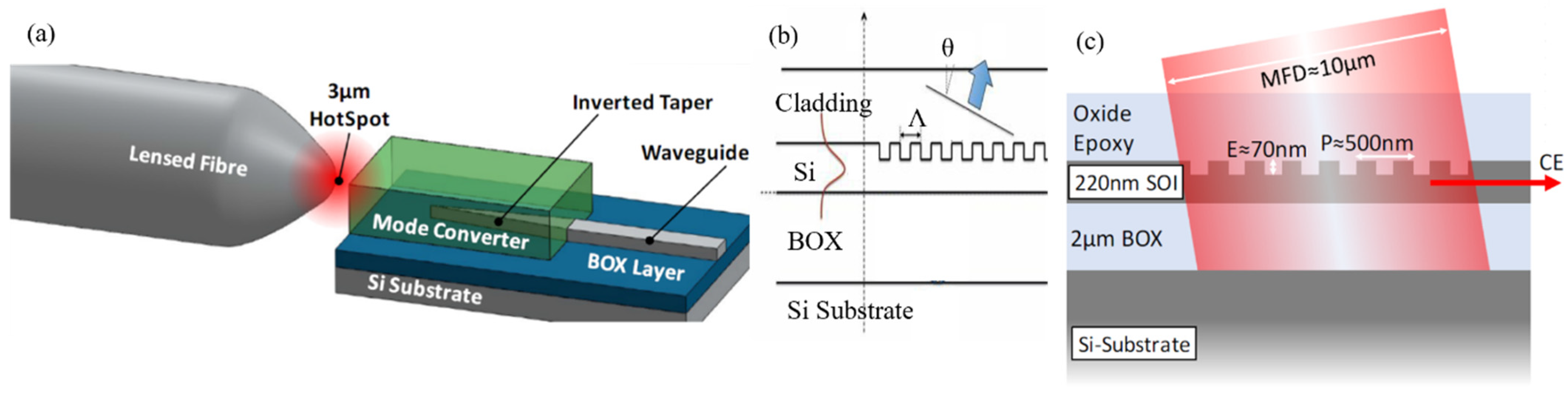
Edge-Coupling
Vertical Grating Couplers
2.1.2. On-Chip Sources
Lasing in Silicon
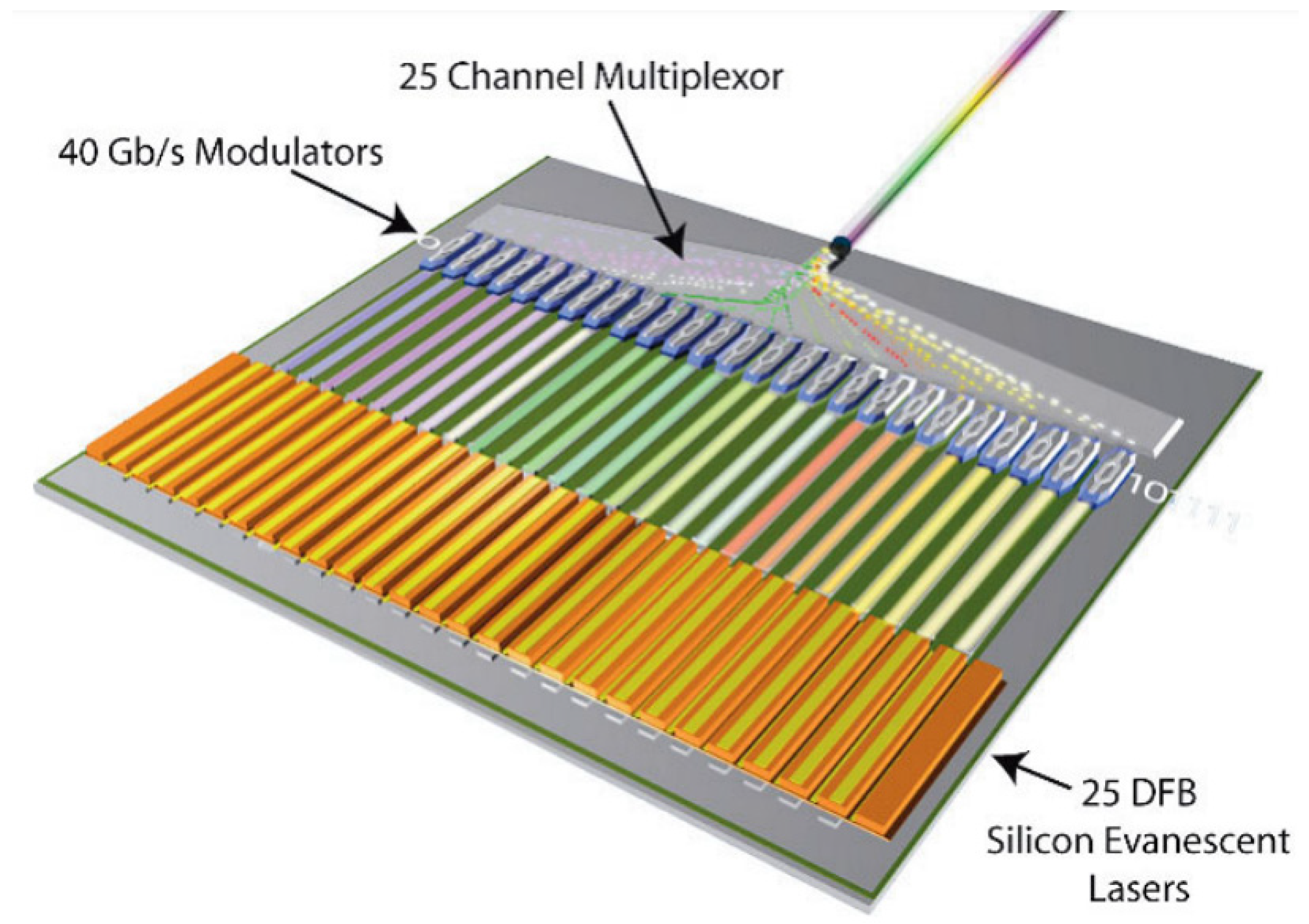
Heterogeneous Integration
External Cavity Lasers
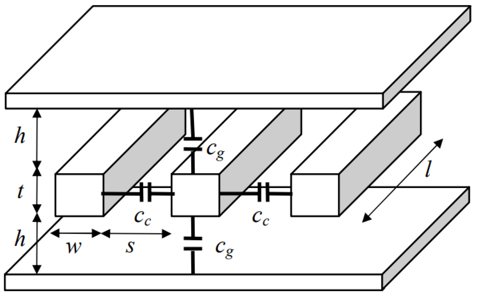
2.2. Waveguide
2.2.1. Towards Sub-100 nm Optical Interconnects
Plasmonic Waveguides
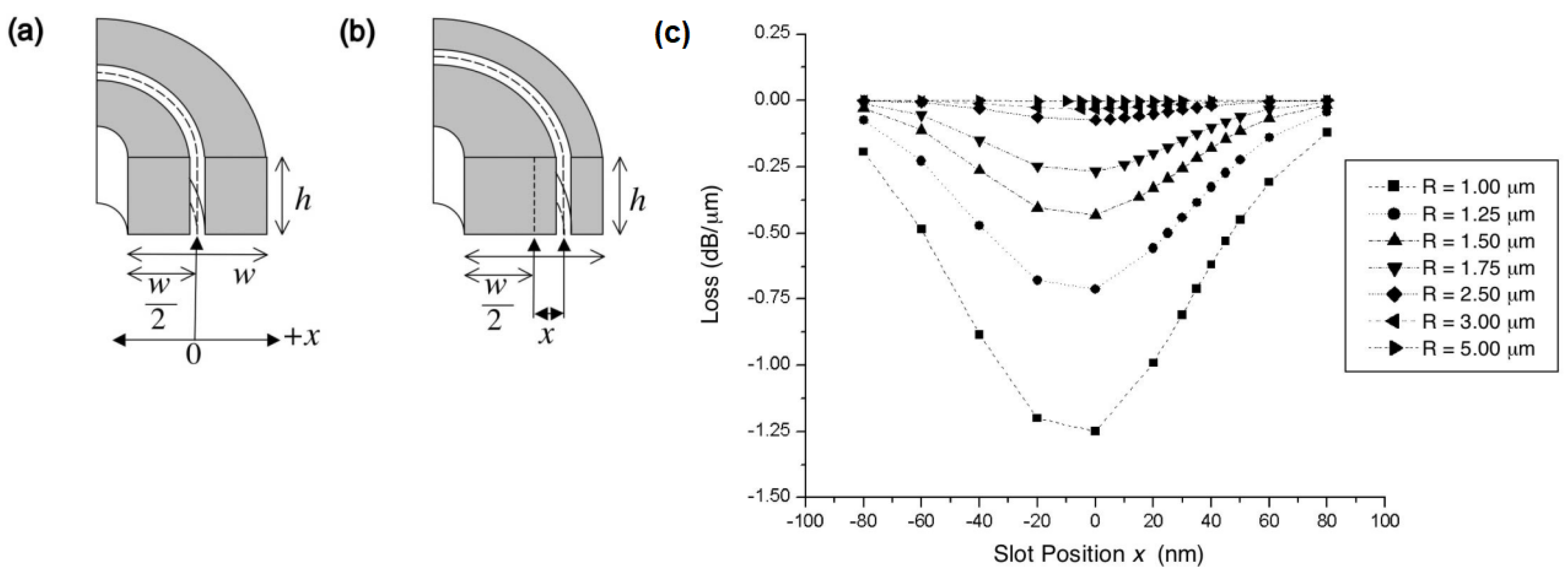
Slot Waveguide
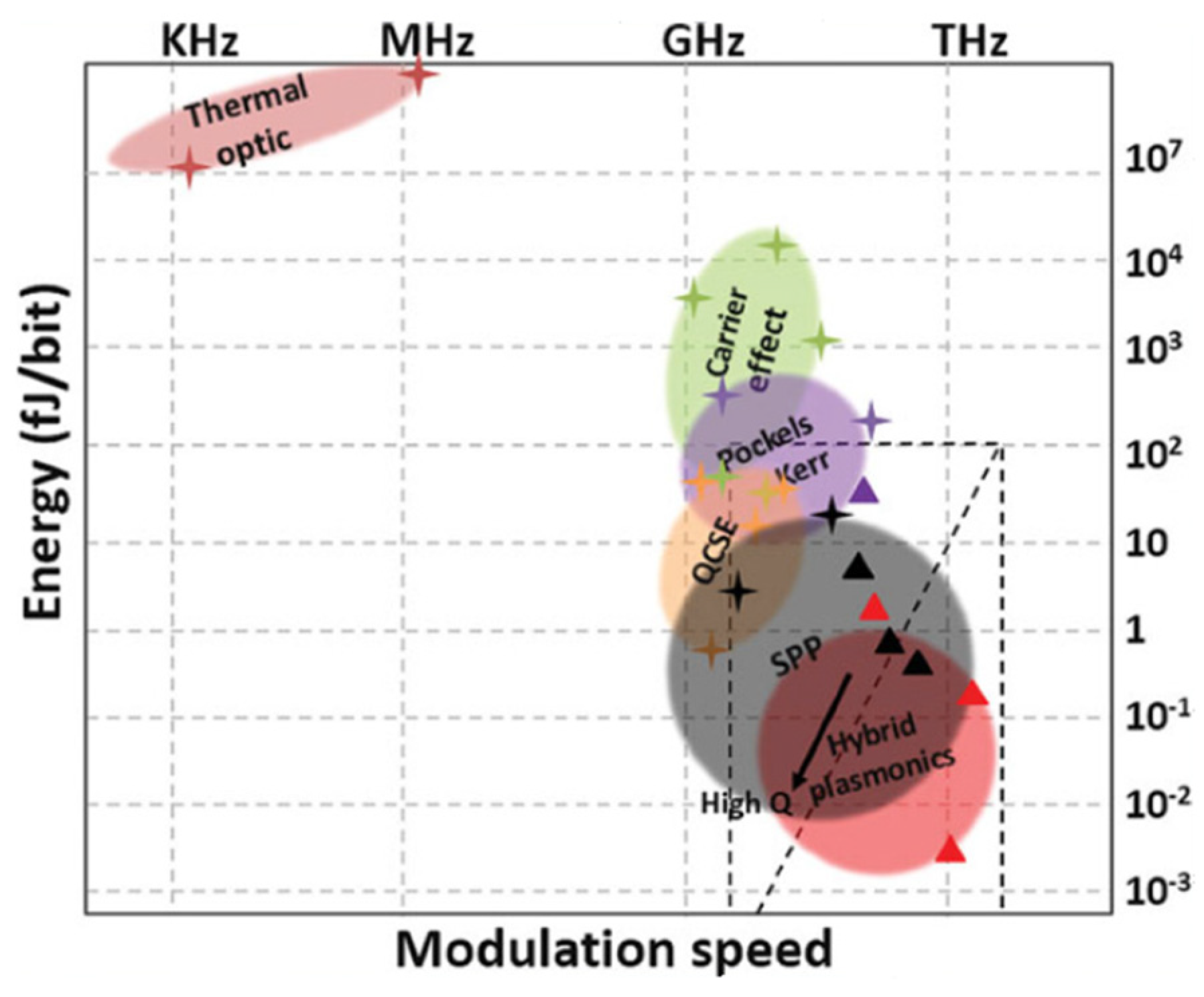
2.3. Modulators
2.3.1. Modulators Performance Metrics
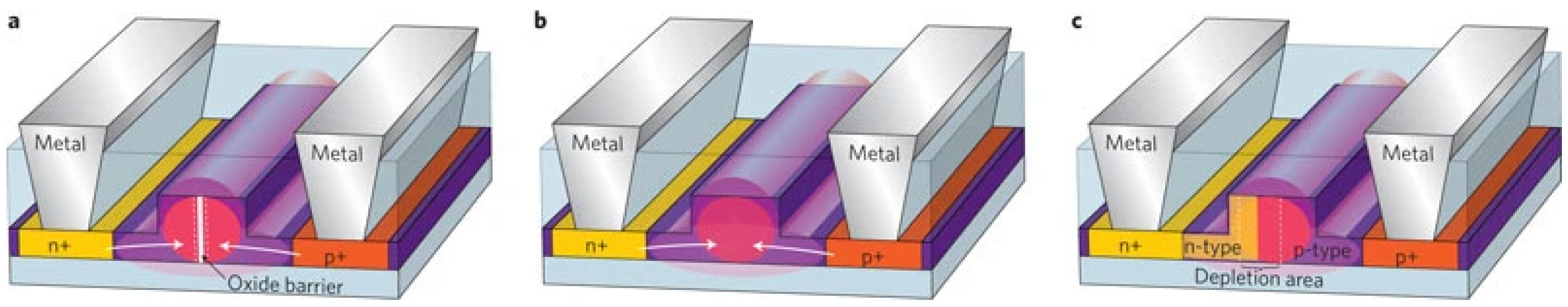
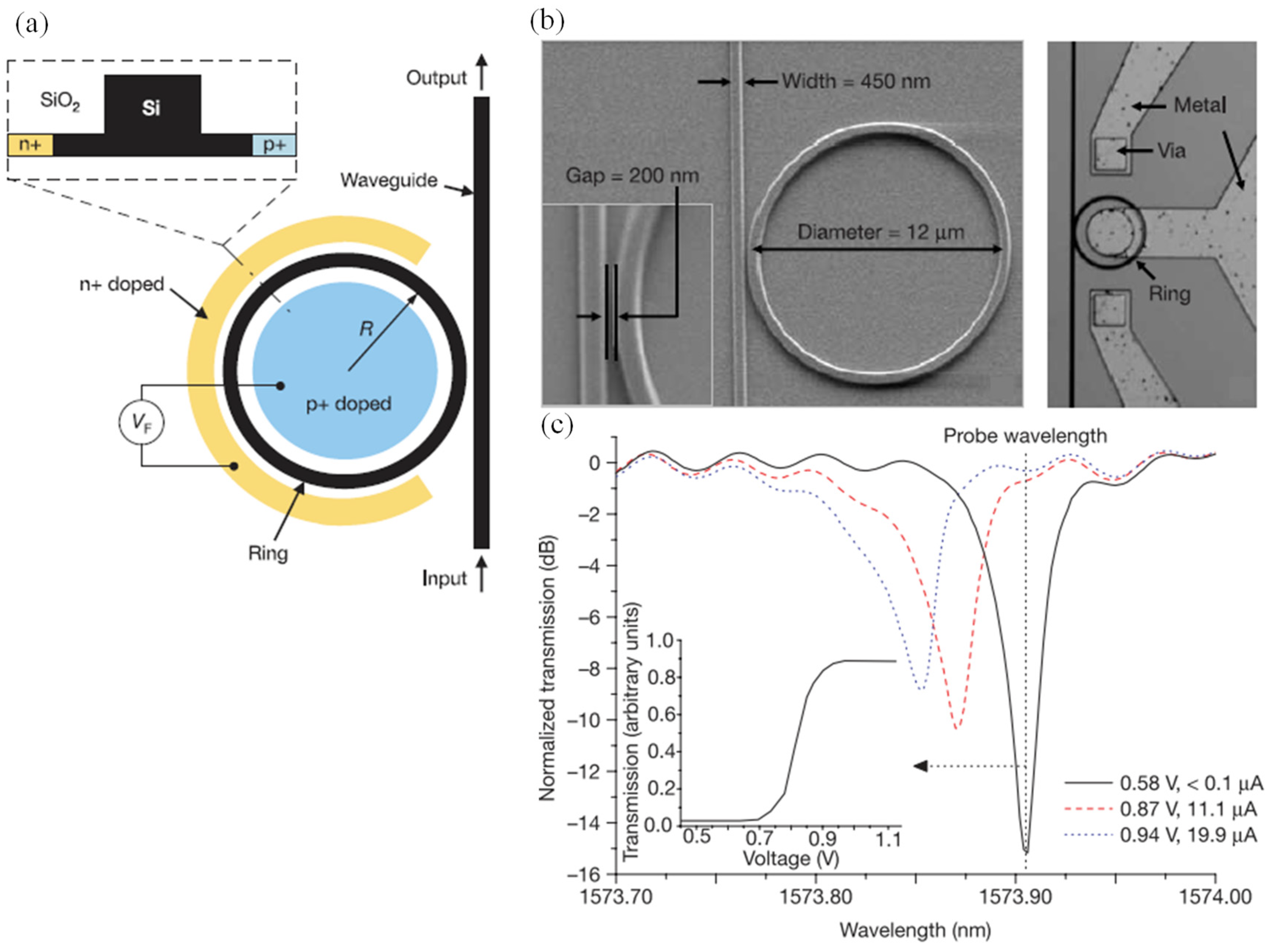
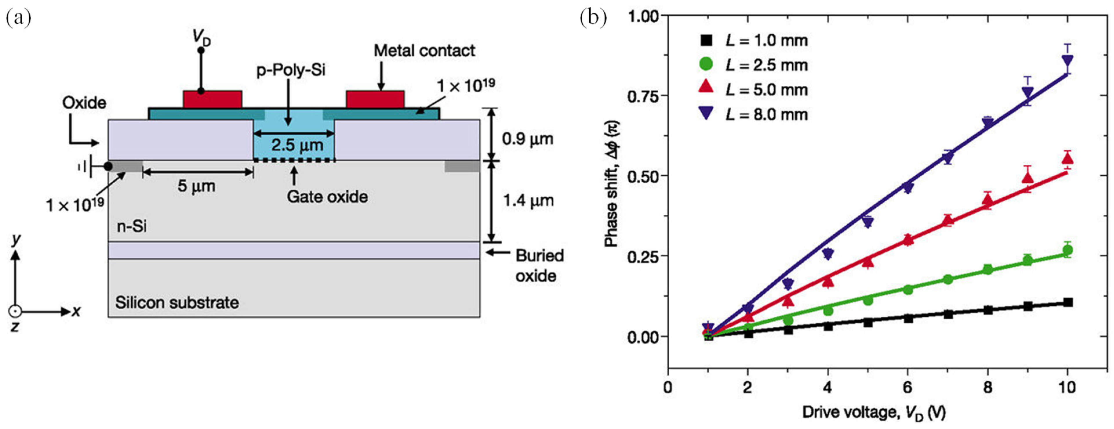
2.3.2. Plasma Dispersion-Based Modulator Configurations
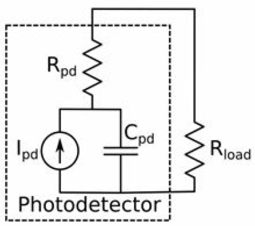
2.4. Photodetectors
2.4.1. Performance Metrics
Responsivity
Speed
Dark Current
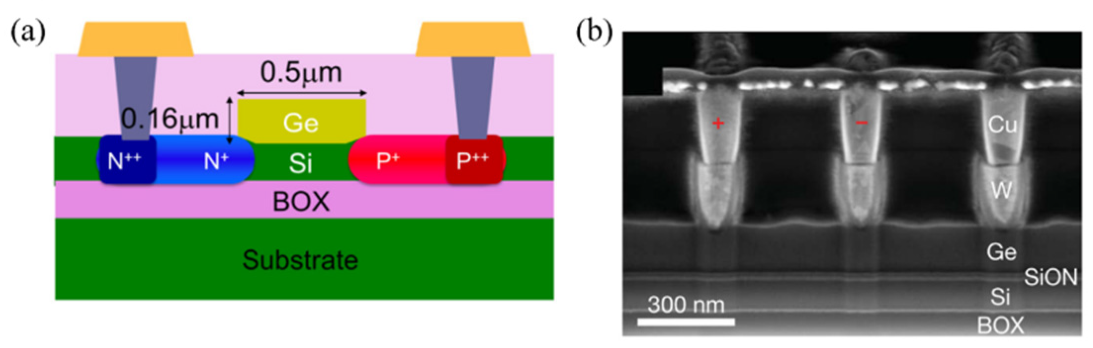
2.4.2. Types of Photodetectors
PIN
Avalanche
2.4.3. Recent Advances
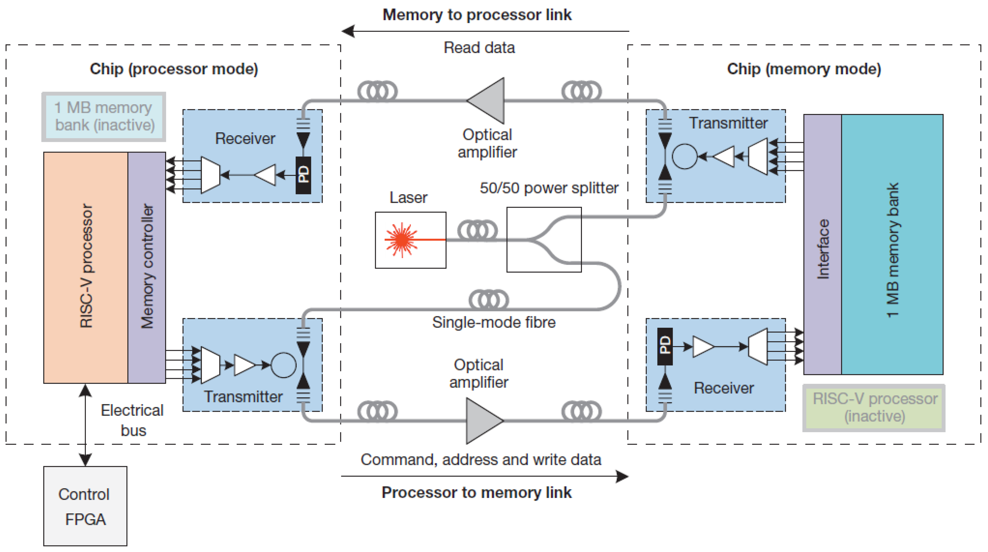
3. Complete Interconnect Systems
4. Conclusions
Author Contributions
Funding
Informed Consent Statement
Conflicts of Interest
References
- The National Technology Roadmap for Semiconductors; Semiconductor Industry Association: Ann Arbor, MA, USA, 1997.
- Warnock, J. Circuit design challenges at the 14 nm technology node. In Proceedings of the 48th Design Automation Conference, San Diego, CA, USA, 5 June 2011. [Google Scholar]
- Ho, R.; Mai, K.; Horowitz, M. Efficient on-chip global interconnects. In Proceedings of the 2003 Symposium on VLSI Circuits. Digest of Technical Papers, Kyoto, Japan, 12–14 June 2003; pp. 271–274. [Google Scholar]
- Ho, R.; Ken, M.; Horowitz, M. Managing wire scaling: A circuit perspective. In Proceedings of the IEEE 2003 International Interconnect Technology Conference, Burlingame, CA, USA, 4 June 2003; pp. 177–179. [Google Scholar]
- John, D.O. Research Challenges for On-Chip Interconnection Networks. 2007, pp. 96–108. Available online: http://doi.ieeecomputersociety.org/10.1109/MM.2007.91 (accessed on 10 December 2021).
- Ho, R.; Mai, K.W.; Horowitz, M.A. The future of wires. In Proceedings of the IEEE; IEEE: Piscataway, NJ, USA, 2001; Volume 89, pp. 490–504. [Google Scholar]
- Ismail, Y.I.; Friedman, E.G.; Neves, J.L. Dynamic and short-circuit power of CMOS gates driving lossless transmission lines. IEEE Transactions on Circuits and Systems I: Fundamental Theory and Applications. In Proceedings of the 8th Great Lakes Symposium on VLSI, Lafayette, LA, USA, 21 February 1998; Volume 46, pp. 950–961. [Google Scholar]
- Ismail, Y.I.; Friedman, E.G. Sensitivity of interconnect delay to on-chip inductance. In Proceedings of the 2000 IEEE International Symposium on Circuits and Systems, Emerging Technologies for the 21st Century. Proceedings (IEEE Cat. No. 00CH36353), Geneva, Switzerland, 28–31 May 2000; Volume 3, pp. 403–406. [Google Scholar]
- Ghoneima, M.; Ismail, Y. Delayed line bus scheme: A low-power bus scheme for coupled on-chip buses. In Proceedings of the 2004 International Symposium on Low Power Electronics and Design, Newport Beach, CA, USA, 9 August 2004. [Google Scholar]
- Ismail, Y.I.; Friedman, E.G. Repeater insertion in RLC lines for minimum propagation delay. In Proceedings of the 1999 IEEE International Symposium on Circuits and Systems (ISCAS), Orlando, FL, USA, 30 May–2 June 1999; Volume 6, pp. 404–407. [Google Scholar]
- Ghoneima, M.; Ismail, Y.; Khellah, M.; De, V. Variation-Tolerant and Low-Power Source-Synchronous Multicycle On-Chip Interconnect Scheme. VLSI Des. 2007, 2007. [Google Scholar] [CrossRef]
- Miller, D.A. Optical interconnects to electronic chips. Appl. Opt. 2010, 49, F59–F70. [Google Scholar] [CrossRef] [PubMed]
- Wilson, L. International Technology Roadmap for Semiconductors (ITRS); Semiconductor Industry Association: Ann Arbor, MA, USA, 2013. [Google Scholar]
- Ghoneima, M.; Ismail, Y.; Khellah, M.; De, V. SSMCB: Low-Power Variation-Tolerant Source-Synchronous Multicycle Bus. In IEEE Transactions on Circuits and Systems I: Regular Papers; IEEE: Piscataway, NJ, USA, 2009; Volume 56, pp. 384–394. [Google Scholar]
- Ghoneima, M.; Ismail, Y.; Khellah, M.; Vivek, D. Reducing the data switching activity on serial link buses. In Proceedings of the 7th International Symposium on Quality Electronic Design (ISQED’06), San Jose, CA, USA, 27–29 March 2006; pp. 6–432. [Google Scholar]
- Ghoneima, M.; Ismail, Y. Utilizing the effect of relative delay on energy dissipation in low-power on-chip buses. IEEE Trans. Very Large Scale Integr. (VLSI) Syst. 2004, 12, 1348–1359. [Google Scholar] [CrossRef][Green Version]
- Bowman, K.; Tschanz, J.; Khellah, M.; Ghoneima, M.; Ismail, Y.; De, V. Time-borrowing multi-cycle on-chip interconnects for delay variation tolerance. In Proceedings of the 2006 International Symposium on Low Power Electronics and Design, Tegernsee, Germany, 4–6 October 2006. [Google Scholar]
- Ghoneima, M.; Ismail, Y. Effect of relative delay on the dissipated energy in coupled interconnects. In Proceedings of the 2004 IEEE International Symposium on Circuits and Systems (IEEE Cat. No. 04CH37512), Vancouver, BC, Canada, 23–26 May 2004. [Google Scholar]
- Ghoneima, M.; Ismail, Y. Optimum positioning of interleaved repeaters in bidirectional buses. IEEE Trans. Comput. -Aided Des. Integr. Circuits Syst. 2004, 24, 461–469. [Google Scholar] [CrossRef]
- Ismail, Y.; Friedman, E.; Neves, J. Repeater insertion in tree structured inductive interconnect. In 1999 IEEE/ACM International Conference on Computer-Aided Design. Digest of Technical Papers (Cat. No. 99CH37051); IEEE: Piscataway, NJ, USA, 2003; Volume 48, pp. 471–481. [Google Scholar]
- Ismail, Y.; Friedman, E. Optimum repeater insertion based on a CMOS delay model for on-chip RLC interconnect. In Proceedings of the Eleventh Annual IEEE International ASIC Conference (Cat. No. 98TH8372); IEEE: Piscataway, NJ, USA, 2002; pp. 369–373. [Google Scholar]
- Magen, N.; Kolodny, A.; Weiser, U.; Shamir, N. Interconnect-power dissipation in a microprocessor. In Proceedings of the 2004 International Workshop on System Level Interconnect Prediction, Paris, France, 14 February 2004. [Google Scholar]
- Ghoneima, M.; Ismail, Y.; Khellah, M.; Tschanz, J.; De, V. Formal derivation of optimal active shielding for low-power on-chip buses. IEEE Trans. Comput. Des. Integr. Circuits Syst. 2006, 25, 821–836. [Google Scholar] [CrossRef]
- Balasubramonian, R.; Muralimanohar, N.; Ramani, K.; Cheng, L.; Carter, J.B. Leveraging Wire Properties at the Microarchitecture Level. IEEE Micro 2006, 26, 40–52. [Google Scholar] [CrossRef]
- Svensson, C. Electrical interconnects revitalized. IEEE Trans. Very Large Scale Integr. (VLSI) Syst. 2002, 10, 777–788. [Google Scholar] [CrossRef]
- Hoppner, S.; Walter, D.; Hocker, T.; Henker, S.; Hanzsche, S.; Sausner, D.; Ellguth, G.; Schlussler, J.-U.; Eisenreich, H.; Schuffny, R. An Energy Efficient Multi-Gbit/s NoC Transceiver Architecture with Combined AC/DC Drivers and Stoppable Clocking in 65 nm and 28 nm CMOS. IEEE J. Solid-State Circuits 2015, 50, 749–762. [Google Scholar] [CrossRef]
- Tadros, R.N.; Ahmed, A.H.; Ghoneima, M.; Ismail, Y. A 24 Gbps SerDes transceiver for on-chip networks using a new half-data-rate self-timed 3-level signaling scheme. In Proceedings of the 5th International Conference on Energy Aware Computing Systems & Applications; IEEE: Piscataway, NJ, USA, 2015; pp. 1–4. [Google Scholar]
- Tadros, R.N.; Elsayed, A.H.; Ghoneima, M.; Ismail, Y. A variation tolerant driving technique for all-digital self-timed 3-level signaling high-speed SerDes transceivers for on-chip networks. In Proceedings of the 2014 IEEE International Symposium on Circuits and Systems (ISCAS); IEEE: Piscataway, NJ, USA, 2014; pp. 1520–1523. [Google Scholar]
- Hussein, E.E.-D.; Safwat, S.; Ghoneima, M.; Ismail, Y. A 16 Gbps low power self-timed SerDes transceiver for multi-core communication. In Proceedings of the 2012 IEEE International Symposium on Circuits and Systems; IEEE: Piscataway, NJ, USA, 2012; pp. 1660–1663. [Google Scholar]
- Safwat, S.; Hussein, E.E.-D.; Ghoneima, M.; Ismail, Y. A 12 Gbps all digital low power SerDes transceiver for on-chip networking. In Proceedings of the 2011 IEEE International Symposium of Circuits and Systems (ISCAS); IEEE: Piscataway, NJ, USA, 2011; pp. 1419–1422. [Google Scholar]
- Hussein, E.E.-D.; Safwat, S.; Ghoneima, M.; Ismail, Y. A new signaling technique for a low power on-chip SerDes transceivers. In Proceedings of the 2010 International Conference on Energy Aware Computing; IEEE: Piscataway, NJ, USA, 2010; pp. 1–2. [Google Scholar]
- Ghoneima, M.; Ismail, Y.; Khellah, M.; Tschanz, J.; De, V. Serial-link bus: A low-power on-chip bus architecture. ICCAD-2005. IEEE/ACM Int. Conf. Comput. -Aided Des. 2005, 56, 2020–2032. [Google Scholar] [CrossRef]
- Miller, D.A.B. Device Requirements for Optical Interconnects to CMOS Silicon Chips. In Integrated Photonics Research, Silicon and Nanophotonics and Photonics in Switching; The Optical Society: Washington, DC, USA, 2010; p. PMB3. [Google Scholar]
- Sievers, G.; Ax, J.; Kucza, N.; Flaskamp, M.; Jungeblut, T.; Kelly, W.; Porrmann, M.; Ruckert, U. Evaluation of interconnect fabrics for an embedded MPSoC in 28 nm FD-SOI. In Proceedings of the 2015 IEEE International Symposium on Circuits and Systems (ISCAS); IEEE: Piscataway, NJ, USA, 2015; pp. 1925–1928. [Google Scholar]
- Ortín-Obón, M.; Suárez-Gracia, D.; Villarroya-Gaudó, M.; Izu, C.; Viñals-Yúfera, V. Analysis of network-on-chip topologies for cost-efficient chip multiprocessors. Microprocess. Microsyst. 2016, 42, 24–36. [Google Scholar] [CrossRef]
- Kumar, R.; Zyuban, V.; Tullsen, D. Interconnections in Multi-Core Architectures: Understanding Mechanisms, Overheads and Scaling. In Proceedings of the 32nd International Symposium on Computer Architecture (ISCA’05); IEEE: Piscataway, NJ, USA, 2005; pp. 408–419. [Google Scholar]
- Esmaeilzadeh, H.; Blem, E.; Amant, R.S.; Sankaralingam, K.; Burger, D. Dark silicon and the end of multicore scaling. ACM SIGARCH Comput. Arch. News 2011, 39, 365–376. [Google Scholar] [CrossRef]
- Geist, A. Supercomputing’s monster in the closet. IEEE Spectr. 2016, 53, 30–35. [Google Scholar] [CrossRef]
- Karkar, A.; Mak, T.; Tong, K.-F.; Yakovlev, A. A Survey of Emerging Interconnects for On-Chip Efficient Multicast and Broadcast in Many-Cores. IEEE Circuits Syst. Mag. 2016, 16, 58–72. [Google Scholar] [CrossRef]
- Carpenter, A.; Hu, J.; Xu, J.; Huang, M.; Wu, H.; Liu, P. Using Transmission Lines for Global On-Chip Communication. IEEE J. Emerg. Sel. Top. Circuits Syst. 2012, 2, 183–193. [Google Scholar] [CrossRef]
- Chang, M.F.; Cong, J.; Kaplan, A.; Naik, M.; Reinman, G.; Socher, E.; Tam, S.-W. CMP network-on-chip overlaid with multi-band RF-interconnect. In Proceedings of the 2008 IEEE 14th International Symposium on High Performance Computer Architecture, Institute of Electrical and Electronics Engineers (IEEE), Salt Lake City, UT, USA, 16–20 February 2008; pp. 191–202. [Google Scholar]
- Zhao, D.; Wang, Y.; Wu, H.; Kikkawa, T. I(Re)2-WiNoC: Exploring scalable wireless on-chip micronetworks for heterogeneous embedded many-core SoCs. Digit. Commun. Netw. 2015, 1, 45–56. [Google Scholar] [CrossRef]
- Mojjada, K.C.; Kim, D.; Eisenstadt, W.R. A 6 pJ/bit transmitter front end in 130 nm CMOS technology for wireless interconnect. In Proceedings of the 2015 IEEE 16th Annual Wireless and Microwave Technology Conference (WAMICON); IEEE: Piscataway, NJ, USA, 2015; pp. 1–3. [Google Scholar]
- Ito, H.; Kimura, M.; Miyashita, K.; Ishii, T.; Okada, K.; Masu, K. A Bidirectional- and Multi-Drop-Transmission-Line Interconnect for Multipoint-to-Multipoint On-Chip Communications. IEEE J. Solid-State Circuits 2008, 43, 1020–1029. [Google Scholar] [CrossRef]
- Coteus, P.W.; Knickerbocker, J.U.; Lam, C.H.; Vlasov, Y.A. Technologies for exascale systems. IBM J. Res. Dev. 2011, 55, 14:1–14:12. [Google Scholar] [CrossRef]
- Caulfield, H.J.; Dolev, S. Why future supercomputing requires optics. Nat. Photon 2010, 4, 261–263. [Google Scholar] [CrossRef]
- Bohnenstiehl, B.; Stillmaker, A.; Pimentel, J.; Andreas, T.; Liu, B.; Tran, A.; Adeagbo, E.; Baas, B. A 5.8 pJ/Op 115 billion ops/sec, to 1.78 trillion ops/sec 32 nm 1000-processor array. In Proceedings of the 2016 IEEE Symposium on VLSI Circuits (VLSI-Circuits); IEEE: Piscataway, NJ, USA, 2016; pp. 1–2. [Google Scholar]
- Popović, M.A.; Wade, M.T.; Orcutt, J.S.; Shainline, J.M.; Sun, C.; Georgas, M.; Moss, B.R.; Kumar, R.; Alloatti, L.; Pavanello, F.; et al. Monolithic silicon photonics in a sub-100 nm SOI CMOS microprocessor foundry: Progress from devices to systems. In Silicon Photonics X; SPIE: Bellingham, WA, USA, 2015; Volume 9367, p. 93670M. [Google Scholar]
- Sun, C.; Georgas, M.; Orcutt, J.; Moss, B.; Chen, Y.H.; Shainline, J.; Wade, M.; Mehta, K.; Nammari, K.; Timurdogan, E.; et al. A monolithically-integrated chip-to-chip optical link in bulk CMOS. Solid-State Circuits IEEE J. 2015, 50, 828–844. [Google Scholar] [CrossRef]
- Heterogeneous Integration Roadmap-Chapter 9. Integrated Photonics; IEEE: Piscataway, NJ, USA, 2021.
- Xu, H.; Dai, D.; Shi, Y. Silicon Integrated Nanophotonic Devices for On-Chip Multi-Mode Interconnects. Appl. Sci. 2020, 10, 6365. [Google Scholar] [CrossRef]
- Dai, D.; Bowers, J.E. Silicon-based on-chip multiplexing technologies and devices for Peta-bit optical interconnects. Nanophotonics 2013, 3, 283–311. [Google Scholar] [CrossRef]
- Daoxin, D.; Zhuoning, Z.; Weike, Z.; Yiwei, X.; Dajian, L. Silicon photonic devices for wavelength/mode-division-multiplexing. Proc. SPIE 2021, 11775, 117750E. [Google Scholar]
- Chrostowski, L.; Hochberg, M. Silicon Photonics Design: From Devices to Systems; Cambridge University Press: Cambridge, UK, 2015. [Google Scholar]
- Agrell, E.; Karlsson, M.; Chraplyvy, A.R.; Richardson, D.J.; Krummrich, P.M.; Winzer, P.; Roberts, K.; Fischer, J.K.; Savory, S.J.; Eggleton, B.J.; et al. Roadmap of optical communications. J. Opt. 2016, 18, 063002. [Google Scholar] [CrossRef]
- Papes, M.; Cheben, P.; Benedikovic, D.; Schmid, J.H.; Pond, J.; Halir, R.; Ortega-Moñux, A.; Wangüemert-Pérez, G.; Winnie, N.Y.; Xu, D.X.; et al. Fiber-chip edge coupler with large mode size for silicon photonic wire waveguides. Opt. Express 2016, 24, 5026–5038. [Google Scholar] [CrossRef]
- McNab, S.J.; Moll, N.; Vlasov, Y. Ultra-low loss photonic integrated circuit with membrane-type photonic crystal waveguides. Opt. Express 2003, 11, 2927–2939. [Google Scholar] [CrossRef]
- Carroll, L.; Lee, J.-S.; Scarcella, C.; Gradkowski, K.; Duperron, M.; Lu, H.; Zhao, Y.; Eason, C.; Morrissey, P.; Rensing, M.; et al. Photonic Packaging: Transforming Silicon Photonic Integrated Circuits into Photonic Devices. Appl. Sci. 2016, 6, 426. [Google Scholar] [CrossRef]
- Vermeulen, D.; Selvaraja, S.K.; Verheyen, P.; Lepage, G.; Bogaerts, W.; Absil, P.; Van Thourhout, D.; Roelkens, G. High-efficiency fiber-to-chip grating couplers realized using an advanced CMOS-compatible Silicon-On-Insulator platform. Opt. Express 2010, 18, 18278–18283. [Google Scholar] [CrossRef]
- Snyder, B.; O’Brien, P. Planar Fiber Packaging Method for Silicon Photonic Integrated Circuits. In Proceedings of the Optical Fiber Communication Conference Postdeadline Papers; The Optical Society: Washington, DC, USA, 2012; p. OM2E.5. [Google Scholar]
- Carroll, L.; Gerace, D.; Cristiani, I.; Menezo, S.; Andreani, L.C. Broad parameter optimization of polarization-diversity 2D grating couplers for silicon photonics. Opt. Express 2013, 21, 21556–21568. [Google Scholar] [CrossRef]
- Dangel, R.; Hofrichter, J.; Horst, F.; Jubin, D.; La Porta, A.; Meier, N.; Soganci, I.M.; Weiss, J.; Offrein, B.J. Polymer waveguides for electro-optical integration in data centers and high-performance computers. Opt. Express 2015, 23, 4736–4750. [Google Scholar] [CrossRef]
- Anderson, P.; Schmidt, B.S.; Lipson, M. High confinement in silicon slot waveguides with sharp bends. Opt. Express 2006, 14, 9197–9202. [Google Scholar] [CrossRef]
- Shoji, T.; Tsuchizawa, T.; Watanabe, T.; Yamada, K.; Morita, H. Low loss mode size converter from 0.3 μm square Si wire waveguides to singlemode fibres. Electron. Lett. 2002, 38, 1669–1670. [Google Scholar] [CrossRef]
- Pu, M.; Liu, L.; Ou, H.; Yvind, K.; Hvam, J.M. Ultra-low-loss inverted taper coupler for silicon-on-insulator ridge waveguide. Opt. Commun. 2010, 283, 3678–3682. [Google Scholar] [CrossRef]
- Hochberg, M.; Harris, N.C.; Ding, R.; Zhang, Y.; Novack, A.; Xuan, Z.; Baehr-Jones, T. Silicon Photonics: The Next Fabless Semiconductor Industry. IEEE Solid-State Circuits Mag. 2013, 5, 48–58. [Google Scholar] [CrossRef]
- Marchetti, R.; Lacava, C.; Khokhar, A.; Cristiani, I.; Richardson, D.; Petropoulos, P.; Minzioni, P. Reflector-less Grating-Coupler with a −0.9 dB Efficiency Realized in 260-nm Silicon-On-Insulator Platform. In Advanced Photonics; The Optical Society: Washington, DC, USA, 2017; pp. 1–2. [Google Scholar]
- Snyder, B.; Corbett, B.; O’Brien, P. Hybrid Integration of the Wavelength-Tunable Laser with a Silicon Photonic Integrated Circuit. J. Light. Technol. 2013, 31, 3934–3942. [Google Scholar] [CrossRef]
- Zheng, X.; Liu, F.; Patil, D.; Thacker, H.; Luo, Y.; Pinguet, T.; Mekis, A.; Yao, J.; Li, G.; Shi, J.; et al. A sub-picojoule-per-bit CMOS photonic receiver for densely integrated systems. Opt. Express 2009, 18, 204–211. [Google Scholar] [CrossRef] [PubMed]
- Sun, C.; Wade, M.T.; Lee, Y.; Orcutt, J.S.; Alloatti, L.; Georgas, M.S.; Waterman, A.S.; Shainline, J.M.; Avizienis, R.R.; Lin, S.; et al. Single-chip microprocessor that communicates directly using light. Nature 2015, 528, 534–538. [Google Scholar] [CrossRef]
- Gunn, C. CMOS Photonics For High Speed Interconnects. ECS Meet. Abstr. 2006, 26, 58–66. [Google Scholar] [CrossRef]
- Painchaud, Y.; Poulin, M.; Pelletier, F.; Latrasse, C.; Gagne, J.-F.; Savard, S.; Robidoux, G.; Picard, M.; Paquet, S.; Davidson, C.; et al. Silicon-based products and solutions. In SPIE OPTO; SPIE: Bellingham, WA, USA, 2014; p. 89880L. [Google Scholar]
- Shen, B.; Wang, P.; Polson, R.; Menon, R. Integrated metamaterials for efficient and compact free-space-to-waveguide coupling. Opt. Express 2014, 22, 27175–27182. [Google Scholar] [CrossRef]
- Cloutier, S.G.; Kossyrev, P.A.; Xu, J. Optical gain and stimulated emission in periodic nanopatterned crystalline silicon. Nat. Mater. 2005, 4, 887–891. [Google Scholar] [CrossRef]
- Pavesi, L.; Negro, L.D.; Mazzoleni, C.; Franzo, G.; Priolo, F. Optical gain in silicon nanocrystals. Nature 2000, 408, 440–444. [Google Scholar] [CrossRef]
- Rong, H.; Liu, A.; Jones, R.; Cohen, O.; Hak, D.; Nicolaescu, R.; Fang, A.; Paniccia, M.J. An all-silicon Raman laser. Nature 2005, 433, 292–294. [Google Scholar] [CrossRef] [PubMed]
- Rong, H.; Xu, S.; Kuo, Y.-H.; Sih, V.; Cohen, O.; Raday, O.; Paniccia, M. Low-threshold continuous-wave Raman silicon laser. Nat. Photon. 2007, 1, 232–237. [Google Scholar] [CrossRef]
- Pralle, M.U.; Moelders, N.; McNeal, M.P.; Puscasu, I.; Greenwald, A.C.; Daly, J.T.; Johnson, E.A.; George, T.; Choi, D.S.; El-Kady, I.; et al. Photonic crystal enhanced narrow-band infrared emitters. Appl. Phys. Lett. 2002, 81, 4685–4687. [Google Scholar] [CrossRef]
- Soref, R. Toward silicon-based longwave integrated optoelectronics (LIO). Silicon Photonics III Int. Soc. Opt. Photonics 2008, 6898, 689809. [Google Scholar]
- Schulz, M. The end of the road for silicon? Nature 1999, 399, 729–730. [Google Scholar] [CrossRef]
- Normile, D. The End--Not Here Yet, But Coming Soon. Science 2001, 293, 787. [Google Scholar] [CrossRef]
- Liu, A.Y.; Zhang, C.; Norman, J.; Snyder, A.; Lubyshev, D.; Fastenau, J.M.; Liu, A.W.K.; Gossard, A.C.; Bowers, J.E. High performance continuous wave 1.3 μm quantum dot lasers on silicon. Appl. Phys. Lett. 2014, 104, 041104. [Google Scholar] [CrossRef]
- Jung, D.; Zhang, Z.; Norman, J.; Herrick, R.; Kennedy, M.J.; Patel, P.; Turnlund, K.; Jan, C.; Wan, Y.; Gossard, A.C.; et al. Highly Reliable Low-Threshold InAs Quantum Dot Lasers on On-Axis (001) Si with 87% Injection Efficiency. ACS Photon. 2018, 5, 1094–1100. [Google Scholar] [CrossRef]
- Chen, S.; Li, W.; Wu, J.; Jiang, Q.; Tang, M.; Shutts, S.; Elliott, S.N.; Sobiesierski, A.; Seeds, A.; Ross, I.; et al. Electrically pumped continuous-wave III–V quantum dot lasers on silicon. Nat. Photon. 2016, 10, 307–311. [Google Scholar] [CrossRef]
- Bowers, J.E.; Komljenovic, T.; Davenport, M.; Hulme, J.; Liu, A.Y.; Santis, C.T.; Spott, A.; Srinivasan, S.; Stanton, E.J.; Zhang, C. Recent advances in silicon photonic integrated circuits. Next-Gener. Opt. Commun. Compon. Sub-Syst. Syst. V 2016, 9774, 977402. [Google Scholar]
- Fang, A.W.; Park, H.; Cohen, O.; Jones, R.; Paniccia, M.J.; Bowers, J.E. Electrically pumped hybrid AlGaInAs-silicon evanescent laser. Opt. Express 2006, 14, 9203–9210. [Google Scholar] [CrossRef] [PubMed]
- Zhang, C.; Liang, D.; Li, C.; Kurczveil, G.; Bowers, J.E.; Beausoleil, R.G. High-speed hybrid silicon microring lasers. In Proceedings of the 2015 IEEE 58th International Midwest Symposium on Circuits and Systems (MWSCAS); IEEE: Piscataway, NJ, USA, 2015; pp. 1–4. [Google Scholar]
- Wang, Y.; Wei, Y.; Huang, Y.; Tu, Y.; Ng, D.; Lee, C.; Zheng, Y.; Liu, B.; Ho, S.-T. Silicon/III-V laser with super-compact diffraction grating for WDM applications in electronic-photonic integrated circuits. Opt. Express 2011, 19, 2006–2013. [Google Scholar] [CrossRef] [PubMed]
- Tran, M.A.; Huang, D.; Guo, J.; Komljenovic, T.; Morton, P.A.; Bowers, J.E. Ring-Resonator Based Widely-Tunable Narrow-Linewidth Si/InP Integrated Lasers. IEEE J. Sel. Top. Quantum Electron. 2020, 26, 1–14. [Google Scholar] [CrossRef]
- Fan, Y.; van Rees, A.; Van der Slot, P.J.M.; Mak, J.; Oldenbeuving, R.M.; Hoekman, M.; Geskus, D.; Roeloffzen, C.G.H.; Boller, K.-J. Hybrid integrated InP-Si3N4 diode laser with a 40-Hz intrinsic linewidth. Opt. Express 2020, 28, 21713–21728. [Google Scholar] [CrossRef]
- Xiang, C.; Guo, J.; Jin, W.; Wu, L.; Peters, J.; Xie, W.; Chang, L.; Shen, B.; Wang, H.; Yang, Q.F.; et al. High-performance lasers for fully integrated silicon nitride photonics. Nat. Commun. 2021, 12, 6650. [Google Scholar] [CrossRef]
- Jin, W.; Yang, Q.-F.; Chang, L.; Shen, B.; Wang, H.; Leal, M.A.; Wu, L.; Gao, M.; Feshali, A.; Paniccia, M.; et al. Hertz-linewidth semiconductor lasers using CMOS-ready ultra-high-Q microresonators. Nat. Photon. 2021, 15, 346–353. [Google Scholar] [CrossRef]
- Koch, B.; Fang, A.; Lively, E.; Jones, R.; Cohen, O.; Blumenthal, D.; Bowers, J. Mode locked and distributed feedback silicon evanescent lasers. Laser Photon. Rev. 2009, 3, 355–369. [Google Scholar] [CrossRef]
- Liu, S.; Wu, X.; Jung, D.; Norman, J.C.; Kennedy, M.J.; Tsang, H.K.; Gossard, A.C.; Bowers, J.E. High-channel-count 20 GHz passively mode-locked quantum dot laser directly grown on Si with 41 Tbit/s transmission capacity. Optica 2019, 6, 128–134. [Google Scholar] [CrossRef]
- Iadanza, S.; Liles, A.; Butler, S.; Hegarty, S.; O’Faolain, L. Photonic crystal lasers: From photonic crystal surface emitting lasers (PCSELs) to hybrid external cavity lasers (HECLs) and topological PhC lasers [Invited]. Opt. Mater. Express 2021, 11, 3245. [Google Scholar] [CrossRef]
- Luo, C.; Zhang, R.; Qiu, B.; Wang, W. Waveguide external cavity narrow linewidth semiconductor lasers. J. Semicond. 2021, 42, 041308. [Google Scholar] [CrossRef]
- Xiang, C.; Jin, W.; Guo, J.; Peters, J.D.; Kennedy, M.J.; Selvidge, J.; Morton, P.A.; Bowers, J.E. Narrow-linewidth III-V/Si/Si3N4 laser using multilayer heterogeneous integration. Optica 2020, 7, 20. [Google Scholar] [CrossRef]
- Xiang, C.; Morton, P.A.; Bowers, J.E. Ultra-narrow linewidth laser based on a semiconductor gain chip and extended Si3N4 Bragg grating. Opt. Lett. 2019, 44, 3825–3828. [Google Scholar] [CrossRef] [PubMed]
- Haurylau, M.; Chen, G.; Chen, H.; Zhang, J.; Nelson, N.A.; Albonesi, D.H.; Friedman, E.G.; Fauchet, P.M. On-Chip Optical Interconnect Roadmap: Challenges and Critical Directions. IEEE J. Sel. Top. Quantum Electron. 2006, 12, 1699–1705. [Google Scholar] [CrossRef]
- Thraskias, C.A.; Lallas, E.N.; Neumann, N.; Schares, L.; Offrein, B.J.; Henker, R.; Plettemeier, D.; Ellinger, F.; Leuthold, J.; Tomkos, I. Survey of Photonic and Plasmonic Interconnect Technologies for Intra-Datacenter and High-Performance Computing Communications. IEEE Commun. Surv. Tutor. 2018, 20, 2758–2783. [Google Scholar] [CrossRef]
- Zhu, S.; Liow, T.Y.; Lo, G.Q.; Kwong, D.L. Silicon-based horizontal nanoplasmonic slot waveguides for on-chip integration. Opt. Express 2011, 19, 8888–8902. [Google Scholar] [CrossRef]
- Dragoman, M.; Dragoman, D. Plasmonics: Applications to nanoscale terahertz and optical devices. Prog. Quantum Electron. 2008, 32, 1–41. [Google Scholar] [CrossRef]
- Vlasov, Y.A.; McNab, S.J. Losses in single-mode silicon-on-insulator strip waveguides and bends. Opt. Express 2004, 12, 1622–1631. [Google Scholar] [CrossRef]
- Bauters, J.F.; Heck, M.J.R.; John, D.; Dai, D.; Tien, M.-C.; Barton, J.S.; Leinse, A.; Heideman, R.G.; Blumenthal, D.J.; Bowers, J.E. Ultra-low-loss high-aspect-ratio Si3N4 waveguides. Opt. Express 2011, 19, 3163–3174. [Google Scholar] [CrossRef]
- Lee, B.G.; Chen, X.; Biberman, A.; Liu, X.; Hsieh, I.W.; Chou, C.Y.; Dadap, J.I.; Xia, F.; Green, W.M.; Sekaric, L.; et al. Ultrahigh-Bandwidth Silicon Photonic Nanowire Waveguides for On-Chip Networks. Photonics Technol. Lett. IEEE 2008, 20, 398–400. [Google Scholar] [CrossRef]
- Li, Z.; Shubin, I.; Zhou, X. Optical interconnects: Recent advances and future challenges. Opt. Express 2015, 23, 3717–3720. [Google Scholar] [CrossRef]
- Bergman, K.; Shalf, J.; Hausken, T. Optical Interconnects and Extreme Computing. Opt. Photonics News 2016, 27, 32–39. [Google Scholar] [CrossRef]
- Rakheja, S.; Kumar, V. Comparison of electrical, optical and plasmonic on-chip interconnects based on delay and energy considerations. In Proceedings of the Thirteenth International Symposium on Quality Electronic Design (ISQED), Santa Clara, CA, USA, 19–21 March 2012; IEEE: Piscataway, NJ, USA, 2012; pp. 732–739. [Google Scholar]
- Wassel, H.M.G.; Dai, D.; Tiwari, M.; Valamehr, J.K.; Theogarajan, L.; Dionne, J.; Chong, F.T.; Sherwood, T. Opportunities and Challenges of Using Plasmonic Components in Nanophotonic Architectures. IEEE J. Emerg. Sel. Top. Circuits Syst. 2012, 2, 154–168. [Google Scholar] [CrossRef]
- Almeida, V.R.; Xu, Q.; Barrios, C.A.; Lipson, M. Guiding and confining light in void nanostructure. Opt. Lett. 2004, 29, 3. [Google Scholar] [CrossRef] [PubMed]
- Xu, Q.; Almeida, V.R.; Panepucci, R.R.; Lipson, M. Experimental demonstration of guiding and confining light in nanometer-size low-refractive-index material. Opt. Lett. 2004, 29, 1626–1628. [Google Scholar] [CrossRef] [PubMed]
- Xiang, C.; Wang, J. Long-Range Hybrid Plasmonic Slot Waveguide. IEEE Photonics J. 2013, 5, 4800311. [Google Scholar] [CrossRef]
- Maier, S. Plasmonics: Fundamentals and Applications; Springer: New York, NY, USA, 2007. [Google Scholar]
- Li, Y.; Cui, K.; Feng, X.; Huang, Y.; Liu, F.; Zhang, W. Ultralow Propagation Loss Slot-Waveguide in High Absorption Active Material. IEEE Photonics J. 2014, 6, 1–6. [Google Scholar] [CrossRef]
- Ishizaka, Y.; Saitoh, K.; Koshiba, M. Transmission-Efficient Structures of Bent and Crossing Silicon Slot Waveguides. IEEE Photonics J. 2013, 5, 6601809. [Google Scholar] [CrossRef]
- Mekawey, H.; Ismail, Y.; Swillam, M. Dynamic routing control through bends for Si sub-micrometer optical interconnects. In Proceedings of the SPIE 10108, Silicon Photonics XII, San Francisco, CA, USA, 20 February 2017. [Google Scholar]
- Peucheret, C. Direct and External Modulation of Light; Department of Photonics Engineering, Technical University of Denmark: Lyngby, Denmark, 2009. [Google Scholar]
- Reed, G.T.; Mashanovich, G.; Gardes, F.Y.; Thomson, D.J. Silicon optical modulators. Nat. Photonics 2010, 4, 518–526. [Google Scholar] [CrossRef]
- Ramdane, A.; Devaux, F.; Souli, N.; Delprat, D.; Ougazzaden, A. Monolithic integration of multiple-quantum-well lasers and modulators for high-speed transmission. IEEE J. Sel. Top. Quantum Electron. 1996, 2, 326–335. [Google Scholar] [CrossRef]
- Tilley, R. Crystals and Crystal Structures; John Wiley: Hoboken, NJ, USA, 2006. [Google Scholar]
- Soref, R.A.; Bennett, B.R. Kramers–Kronig analysis of electro-optical switching in silicon. SPIE Integr. Opt. Circuit Eng. IV 1987, 704, 7. [Google Scholar]
- Clark, S.A.; Culshaw, B.; Dawnay, E.J.C.; Day, I.E. Thermo-optic phase modulators in SIMOX material. Symp. Integr. Optoelectron. 2000, 3936, 16–24. [Google Scholar] [CrossRef]
- Shainline, J.M.; Orcutt, J.S.; Wade, M.T.; Nammari, K.; Moss, B.; Georgas, M.; Sun, C.; Ram, R.J.; Stojanović, V.; Popović, M.A. Depletion-mode carrier-plasma optical modulator in zero-change advanced CMOS. Opt. Lett. 2013, 38, 3. [Google Scholar] [CrossRef] [PubMed]
- Lee, J.-M.; Kim, D.-J.; Kim, G.-H.; Kwon, O.-K.; Kim, K.-J.; Kim, G. Controlling temperature dependence of silicon waveguide using slot structure. Opt. Express 2008, 16, 1645–1652. [Google Scholar] [CrossRef] [PubMed]
- Teng, J.; Dumon, P.; Bogaerts, W.; Zhang, H.; Jian, X.; Han, X.; Zhao, M.; Morthier, G.; Baets, R. Athermal Silicon-on-insulator ring resonators by overlaying a polymer cladding on narrowed waveguides. Optics Express 2009, 17, 14627–14633. [Google Scholar] [CrossRef]
- Barrios, C.A.; Almeida, V.R.; Panepucci, R.; Lipson, M. Electrooptic modulation of silicon-on-insulator submicrometer-size waveguide devices. J. Lightwave Technol. 2003, 21, 8. [Google Scholar] [CrossRef]
- Cutolo, A.; Iodice, M.; Spirito, P.; Zeni, L. Silicon electro-optic modulator based on a three terminal device integrated in a low-loss single-mode SOI waveguide. J. Lightwave Technol. 1997, 15, 14. [Google Scholar] [CrossRef]
- Cutolo, A.; Iodice, M.; Irace, A.; Spirito, P.; Zeni, L. An electrically controlled Bragg reflector integrated in a rib silicon on insulator waveguide. Appl. Phys. Lett. 1997, 71, 3. [Google Scholar] [CrossRef]
- Dainesi, P.; Kung, A.; Chabloz, M.; Lagos, A.; Fluckiger, P.; Ionescu, A.; Fazan, P.; Declerq, M.; Renaud, P.; Robert, P. CMOS compatible fully integrated Mach-Zehnder interferometer in SOI technology. IEEE Photonics Technol. Lett. 2000, 12, 660–662. [Google Scholar] [CrossRef]
- Friedman, L.; Soref, R.A.; Lorenzo, J.P. Silicon double-injection electrooptic modulator with junction gate control. J. Appl. Phys. 1988, 63, 9. [Google Scholar] [CrossRef]
- Hewitt, P.D.; Reed, G.T. Multi micron dimension optical p-i-n modulators in silicon-on-insulator. SPIE 1999, 3630, 237–243. [Google Scholar]
- Hewitt, P.D.; Reed, G.T. Improving the response of optical phase modulators in SOI by computer simulation. J. Lightwave Technol. 2000, 18, 8. [Google Scholar] [CrossRef]
- Jackson, S.M.; Reed, G.T.; Tang, C.K.; Evans, A.G.R.; Clark, J.; Aveyard, C.; Namavar, F. Optical beamsteering using integrated optical modulators. J. Lightwave Technol. 1997, 15, 2259–2263. [Google Scholar] [CrossRef]
- Jackson, S.M.; Hewitt, P.D.; Reed, G.T.; Tang, C.K.; Evans, A.G.R.; Clark, J.; Aveyard, C.; Namavar, F. A novel optical phase modulator design suitable for phased arrays. J. Lightwave Technol. 1998, 16, 2016. [Google Scholar] [CrossRef]
- Lorenzo, J.P.; Soref, R.A. 1.3 μm electro-optic silicon switch. Appl. Phys. Lett. 1987, 51, 3. [Google Scholar] [CrossRef]
- Van Camp, M.A.; Assefa, S.; Gill, D.M.; Barwicz, T.; Shank, S.M.; Rice, P.M.; Topuria, T.; Green, W.M.J. Demonstration of electrooptic modulation at 2165 nm using a silicon Mach-Zehnder interferometer. Opt. Express 2012, 20, 8. [Google Scholar] [CrossRef]
- Png, C.E.; Chan, S.P.; Lim, S.T.; Reed, G.T. Optical phase modulators for MHz and GHz modulation in silicon-on-insulator (SOI). J. Lightwave Technol. 2004, 22, 10. [Google Scholar] [CrossRef]
- Wu, R.; Chen, C.H.; Huang, T.C.; Cheng, K.T.; Beausoleil, R. 20 Gb/s carrier-injection silicon microring modulator with SPICE-compatible dynamic model. In Proceedings of the 2015 International Conference on Photonics in Switching (PS), Florence, Italy, 22–25 September 2015. [Google Scholar]
- Sciuto, A.; Libertino, S.; Alessandria, A.; Coffa, S.; Coppola, G. Design, fabrication, and testing of an integrated Si-based light modulator. J. Lightwave Technol. 2003, 21, 6. [Google Scholar] [CrossRef]
- Tang, C.K.; Reed, G.T.; Wilson, A.J.; Rickman, A.G. Simulation of a low loss optical modulator for fabrication in SIMOX material. Symp. Mater. Res. Soc. 1993, 298, 247–252. [Google Scholar] [CrossRef]
- Tang, C.K.; Reed, G.T.; Wilson, A.J.; Rickman, A.G. Low-loss, singlemodel optical phase modulator in SIMOX material. J. Lightwave Technol. 1994, 12, 7. [Google Scholar] [CrossRef]
- Tang, C.K.; Reed, G.T. Highly efficient optical phase modulator in SOI waveguides. Electron. Lett. 1995, 31, 2. [Google Scholar] [CrossRef]
- Treyz, G.V. Silicon Mach–Zehnder waveguide interferometers operating at 1.3 μm. Electron. Lett. 1991, 27, 3. [Google Scholar] [CrossRef]
- Treyz, G.V.; May, P.G.; Halbout, J.-M. Silicon optical modulators at 1.3-μm based on free-carrier absorption. IEEE Electr. Device Lett. 1991, 12, 3. [Google Scholar] [CrossRef]
- Day, I.E.; Roberts, S.W.; O’Carroll, R.; Knights, A.; Sharp, P.; Hopper, G.F.; Luff, B.J.; Asghari, M. Single-Chip Variable Optical Attenuator and Multiplexer Subsystem Integration. In Proceedings of the Optical Fiber Communication Conference and Exhibit, Anaheim, CA, USA, 17–22 March 2002; p. TuK4. [Google Scholar]
- Kim, J.F.Y.; Takahashi, S.; Takenaka, M.; Takagi, S. SiGe-based carrier-injection Mach-Zehnder modulator with enhanced plasma dispersion effect in strained SiGe. In Proceedings of the 2015 Optical Fiber Communications Conference and Exhibition (OFC), Los Angeles, CA, USA, 22–26 March 2015. [Google Scholar]
- Xu, Q.; Schmidt, B.; Pradhan, S.; Lipson, M. Micrometre-scale silicon electro-optic modulator. Nature 2005, 435, 325. [Google Scholar] [CrossRef] [PubMed]
- Liu, K.; Ye, C.R.; Khan, S.; Sorger, V.J. Review and perspective on ultrafast wavelength-size electro-optic modulators. Laser Photonics Rev. 2015, 9, 172–194. [Google Scholar] [CrossRef]
- Krückel, H.B.C.J.; Ban, Y.; Heck, M.J.R.; van Campenhout, J.; van Thourhout, D. Towards Maximum Energy Efficiency of Carrier-Injection-Based Silicon Photonics. J. Lightwave Technol. 2021, 39, 2931–2940. [Google Scholar] [CrossRef]
- Liu, A.; Jones, R.; Liao, L.; Samara-Rubio, D.; Rubin, D.; Cohen, O.; Nicolaescu, R.; Paniccia, M. A high-speed silicon optical modulator based on a metal–oxide–semiconductor capacitor. Nature 2004, 427, 615–618. [Google Scholar] [CrossRef] [PubMed]
- Liao, L.; Samara-Rubio, D.; Morse, M.; Liu, A.; Hodge, D.; Rubin, D.; Keil, U.D.; Franck, T. High speed silicon Mach-Zehnder modulator. Opt. Express 2005, 13, 3129–3135. [Google Scholar] [CrossRef] [PubMed]
- Kajikawa, K.; Tabei, T.; Sunami, H. An infrared silicon optical modulator of metal-oxide-semiconductor capacitor based on accumulation-carrier absorption. Jpn. J. Appl. Phys. 2009, 48, 04C107. [Google Scholar] [CrossRef]
- Alloatti, L.; Palmer, R.; Diebold, S.; Pahl, K.P.; Chen, B.; Dinu, R.; Fournier, M.; Fedeli, J.-M.; Zwick, T.; Freude, W.; et al. 100 GHz silicon–organic hybrid modulator. Light Sci. Appl. 2014, 3, 4. [Google Scholar] [CrossRef]
- Sodagar, M.; Hosseinnia, A.H.; Isautier, P.; Moradinejad, H.; Ralph, S.; Eftekhar, A.A.; Adibi, A. Compact, 15 Gb/s electro-optic modulator through carrier accumulation in a hybrid Si/SiO2/Si microdisk. Opt Express 2015, 23, 28306–28315. [Google Scholar] [CrossRef]
- Reed, G.T.; Mashanovich, G.Z.; Gardes, F.Y.; Nedeljkovic, M.; Hu, Y.; Thomson, D.J.; Li, K.; Wilson, P.R.; Chen, S.; Hsu, S.S. Recent breakthroughs in carrier depletion based silicon optical modulators. Nanophotonics 2013, 3, 17. [Google Scholar] [CrossRef]
- Gardes, F.Y.; Reed, G.T.; Emerson, N.; Png, C. A sub-micron depletiontype photonic modulator in silicon on insulator. Opt. Express 2005, 13, 10. [Google Scholar] [CrossRef]
- Liu, A.; Liao, L.; Rubin, D.; Nguyen, H.; Ciftcioglu, B.; Chetrit, Y.; Izhaky, N.; Paniccia, M. High-speed optical modulation based on carrier depletion in a silicon waveguide. Opt. Express. 2007, 15, 9. [Google Scholar] [CrossRef] [PubMed]
- Liao, L.; Liu, A.; Rubin, D.; Basak, J.; Chetrit, Y.; Nguyen, H.; Cohen, R.; Izhaky, N.; Paniccia, M. 40 Gbit/s silicon optical modulator for highspeed applications. Electron Lett. 2007, 43, 2. [Google Scholar] [CrossRef]
- Spector, S.J.; Geis, M.W.; Grein, M.E.; Schulein, R.T.; Yoon, J.U.; Lennon, D.M.; Gan, F.; Zhou, G.-R.; Kaertner, F.X.; Lyszczarz, T.M. High-speed silicon electro-optical modulator that can be operated in carrier depletion or carrier injection mode. In Proceedings of the 2008 Conference on Lasers and Electro-Optics and 2008 Conference on Quantum Electronics and Laser Science, San Jose, CA, USA, 4–9 May 2008. [Google Scholar]
- Marris-Morini, D.; Vivien LFédéli, J.-M.; Cassan, E.; Lyan, P.; Laval, S. Low loss and high speed silicon optical modulation based on a lateral carrier depletion structure. Opt. Express 2008, 16, 6. [Google Scholar] [CrossRef] [PubMed]
- You, J.-B.; Park, M.; Park, J.-W.; Kim, G. 12.5 Gbps optical modulation of silicon racetrack resonator based on carrier-depletion in asymmetric p-n diode. Opt. Express 2008, 16, 5. [Google Scholar] [CrossRef] [PubMed]
- Li, G.; Zheng, X.; Thacker, H.; Yao, J.; Loo, Y.; Shubin, I.; Raj, K.; Cunningham, J.E.; Krishnamoorthy, A.V. 40 Gb/s Thermally Tunable CMOS ring Modulator. In Proceedings of the 9th International Conference on Group IV Photonics (GFP), San Diego, CA, USA, 29–31 August 2012. [Google Scholar]
- Korn, D.; Yu, H.; Hillerkuss, D.; Alloatti, L.; Mattern, C.; Komorowska, K.; Bogaerts, W.; Baets, R.; Van Campenhout, J.; Verheyen, P.; et al. Detection or modulation at 35 Gbit/s with a Standard CMOS-processed Optical Waveguide. In Proceedings of the 2012 Conference Conference on Lasers and electro-Optics (CLEO), San Jose, CA, USA, 6–11 May 2012. [Google Scholar]
- Dong, P.; Chen, L.; Chen, Y.-K. High-speed low-voltage single-drive push-pull silicon Mach-Zehnder modulators. Opt. Express 2012, 20, 7. [Google Scholar] [CrossRef] [PubMed]
- Timurdogan, E.; Sorace-Agaskar, C.M.; Sun, J.; Hosseini, E.S.; Biberman, A.; Watts, M.R. An ultralow power athermal silicon modulator. Nat. Commun. 2014, 5, 4008. [Google Scholar] [CrossRef]
- Gehl, M.; Long, C.; Trotter, D.; Starbuck, A.; Pomerene, A.; Wright, J.B.; Melgaard, S.; Siirola, J.; Lentine, A.L.; DeRose, C. Operation of high-speed silicon photonic micro-disk modulators at cryogenic temperatures. Optica 2017, 4, 374–382. [Google Scholar] [CrossRef]
- Gostimirovic, D.; Ye, W.N. Ultralow-Power Double Vertical Junction Microdisk Modulators. IEEE J. Sel. Top. Quantum Electron. 2021, 27, 1–7. [Google Scholar] [CrossRef]
- Li, E.; Gao, Q.; Liverman, S.; Wang, A.X. One-volt silicon photonic crystal nanocavity modulator with indium oxide gate. Opt. Lett. 2018, 43, 4429–4432. [Google Scholar] [CrossRef]
- Li, E.; Gao, Q.; Chen, R.T.; Wang, A.X. Ultracompact Silicon-Conductive Oxide Nanocavity Modulator with 0.02 Lambda-Cubic Active Volume. Nano Letters 2018, 18, 1075–1081. [Google Scholar] [CrossRef] [PubMed]
- Meister, S.; Rhee, H.; Al-Saadi, A.; Franke, B.A.; Kupijai, S.; Theiss, C.; Zimmermann, L.; Tillack, B.; Richter, H.H.; Tian, H.; et al. Matching p-i-n-junctions and optical modes enables fast and ultra-small silicon modulators. Opt. Express 2013, 21, 16210–16221. [Google Scholar] [CrossRef]
- Shakoor, A.; Nozaki, K.; Kuramochi, E.; Nishiguchi, K.; Shinya, A.; Notomi, M. Compact 1D-silicon photonic crystal electro-optic modulator operating with ultra-low switching voltage and energy. Optics Express 2014, 22, 28623–28634. [Google Scholar] [CrossRef]
- Zhang, J.; Leroux, X.; Durán-Valdeiglesias, E.; Alonso-Ramos, C.; Marris-Morini, D.; Vivien, L.; He, S.; Cassan, E. Generating Fano Resonances in a Single-Waveguide Silicon Nanobeam Cavity for Efficient Electro-Optical Modulation. ACS Photonics 2018, 5, 4229–4237. [Google Scholar] [CrossRef]
- Li, E.; Wang, A.X. Theoretical Analysis of Energy Efficiency and Bandwidth Limit of Silicon Photonic Modulators. J. Lightwave Technol. 2019, 37, 5801–5813. [Google Scholar] [CrossRef]
- Buckwalter, J.F.; Zheng, X.; Li, G.; Raj, K.; Krishnamoorthy, A.V. A Monolithic 25-Gb/s Transceiver with Photonic Ring Modulators and Ge Detectors in a 130-nm CMOS SOI Process. IEEE J. Solid-State Circuits 2012, 47, 1309–1322. [Google Scholar] [CrossRef]
- Hsu, Y.; Tzu, T.C.; Lin, T.C.; Chuang, C.Y.; Wu, X.; Chen, J.; Yeh, C.H.; Tsang, H.K.; Chow, C.W. 64-Gbit/s PAM-4 20-km transmission using silicon micro-ring modulator for optical access networks. In Proceedings of the 2017 Optical Fiber Communications Conference and Exhibition (OFC), Los Angeles, CA, USA, 19–23 March 2017; pp. 1–3. [Google Scholar]
- Ding, Y.; Zhu, X.; Xiao, S.; Hu, H.; Frandsen, L.H.; Mortensen, N.A.; Yvind, K. Effective Electro-Optical Modulation with High Extinction Ratio by a Graphene–Silicon Microring Resonator. Nano Lett. 2015, 15, 4393–4400. [Google Scholar] [CrossRef] [PubMed]
- Dubé-Demers, R.; LaRochelle, S.; Shi, W. Ultrafast pulse-amplitude modulation with a femtojoule silicon photonic modulator. Optica 2016, 3, 622–627. [Google Scholar] [CrossRef]
- Sinatkas, G.; Christopoulos, T.; Tsilipakos, O.; Kriezis, E.E. Electro-optic modulation in integrated photonics. J. Appl. Phys. 2021, 130, 010901. [Google Scholar] [CrossRef]
- Watts, M.R.; Zortman, W.A.; Trotter, D.C.; Young, R.W.; Lentine, A.L. Vertical junction silicon microdisk modulators and switches. Opt. Express 2011, 19, 21989–22003. [Google Scholar] [CrossRef]
- Xiao, X.; Xu, H.; Li, X.; Hu, Y.; Xiong, K.; Li, Z.; Chu, T.; Yu, Y.; Yu, J. 25 Gbit/s silicon microring modulator based on misalignment-tolerant interleaved PN junctions. Opt. Express 2012, 20, 2507–2515. [Google Scholar] [CrossRef]
- Campenhout, J.V.; Pantouvaki, M.; Verheyen, P.; Selvaraja, S.; Lepage, G.; Yu, H.; Lee, W.; Wouters, J.; Goossens, D.; Moelants, M.; et al. Low-voltage, low-loss, multi-Gb/s silicon micro-ring modulator based on a MOS capacitor. In Proceedings of the OFC/NFOEC, Los Angeles, CA, USA, 4–8 March 2012; pp. 1–3. [Google Scholar]
- Dong, P.; Liao, S.; Feng, D.; Liang, H.; Zheng, D.; Shafiiha, R.; Kung, C.C.; Qian, W.; Li, G.; Zheng, X.; et al. Low Vpp, ultralow-energy, compact, high-speed silicon electro-optic modulator. Opt. Express 2009, 17, 22484–22490. [Google Scholar] [CrossRef]
- Gunn, G.M.C.; Witzens, J.; Capellini, G. CMOS photonics using germanium photodetectors. ECS Trans. 2006, 3, 8. [Google Scholar] [CrossRef]
- Park, A.W.F.H.; Jones, R.; Cohen, O.; Raday, O.; Sysak, M.N.; Paniccia, M.J.; Bowers, J.E. A hybrid AlGaInAs-silicon evanescent waveguide photodetector. Opt. Express 2007, 15, 9. [Google Scholar] [CrossRef] [PubMed]
- Baehr-Jones, R.D.T.; Ayazi, A.; Pinguet, T.; Streshinsky, M.; Harris, N.; Li, J.; He, L.; Gould, M.; Zhang, Y.; Lim, A.E.; et al. A 25 Gb/s Silicon Photonics Platform. arXiv 2012, arXiv:1203.0767. [Google Scholar]
- Vivien, J.O.L.; Fédéli, J.-M.; Marris-Morini, D.; Crozat, P.; Damlencourt, J.-F.; Cassan, E.; Lecunff, Y.; Laval, S. 42 GHz p.i.n Germanium photodetector integrated in a silicon-on-insulator waveguide. Opt. Express 2009, 17, 6. [Google Scholar] [CrossRef] [PubMed]
- Binetti, P.R.A.; Leijtens, X.J.M.; de Vries, T.; Oei, Y.S.; di Cioccio, L.; Fedeli, J.-M.; Lagahe, C.; van Campenhout, J.; van Thourhout, D.; van Veldhoven, P.J.; et al. InP/InGaAs Photodetector on SOI Circuitry. In Proceedings of the 2009 6th IEEE International Conference on Group IV Photonics, San Francisco, CA, USA, 9–11 September 2009. [Google Scholar]
- Nagarajan, R.; Rahn, J.; Kato, M.; Pleumeekers, J.; Lambert, D.; Lal, V.; Tsai, H.S.; Nilsson, A.; Dentai, A.; Kuntz, M.; et al. 10 Channel, 45.6 Gb/s per Channel, Polarization-Multiplexed DQPSK, InP Receiver Photonic Integrated Circuit. J. Lightwave Technol. 2011, 29, 386–395. [Google Scholar] [CrossRef]
- Bradley, J.D.B.; Jessop, P.E.; Knights, A.P. Silicon waveguide-integrated optical power monitor with enhanced sensitivity at 1550 nm. Appl. Phys. Lett. 2005, 86, 241103. [Google Scholar] [CrossRef]
- Geis, S.J.S.M.W.; Grein, M.E.; Schulein, R.T.; Yoon, J.U.; Lennon, D.M.; Deneault, S.; Gan, F.; Kaertner, F.X.; Lyszczarz, T.M. CMOS-Compatible All-Si High-Speed Waveguide Photodiodes with High Responsivity in Near-Infrared Communication Band. IEEE Photon. Technol. Lett. 2013, 19, 3. [Google Scholar] [CrossRef]
- Grote, K.P.R.R.; Souhan, B.; Driscoll, J.B.; Bergman, K.; Osgood, R.M., Jr. 10 Gb/s Error-Free Operation of All-Silicon Ion-Implanted-Waveguide Photodiodes at 1.55 µm. IEEE Photon. Technol. Lett. 2013, 25, 4. [Google Scholar] [CrossRef]
- Souhan, R.R.G.B.; Driscoll, J.B.; Lu, M.; Stein, A.; Bakhru, H.; Osgood, R.M. Metal-semiconductormetal ion-implanted Si waveguide photodetectors for C-band operation. Opt. Express 2014, 22, 9. [Google Scholar] [CrossRef] [PubMed]
- Donati, S. Photodetectors: Devices, Circuits and Applications, 2nd ed.; Wiley-IEEE Press: Hoboken, NJ, USA, 2021. [Google Scholar]
- Chen, H.; Verheyen, P.; De Heyn, P.; Lepage, G.; De Coster, J.; Balakrishnan, S.; Absil, P.; Yao, W.; Shen, L.; Roelkens, G.; et al. −1 V bias 67 GHz bandwidth Si-contacted germanium waveguide p-i-n photodetector for optical links at 56 Gbps and beyond. Opt. Express 2016, 24, 4622–4631. [Google Scholar] [CrossRef] [PubMed]
- Mehta, K.K.; Orcutt, J.S.; Shainline, J.M.; Tehar-Zahav, O.; Sternberg, Z.; Meade, R.; Popović, M.A.; Ram, R.J. Polycrystalline silicon ring resonator photodiodes in a bulk complementary metal-oxide-semiconductor process. Opt. Lett. 2014, 39, 1061–1064. [Google Scholar] [CrossRef] [PubMed]
- Lischke, S.; Peczek, A.; Morgan, J.S.; Sun, K.; Steckler, D.; Yamamoto, Y.; Korndörfer, F.; Mai, C.; Marschmeyer, S.; Fraschke, M.; et al. Ultra-fast germanium photodiode with 3-dB bandwidth of 265 GHz. Nat. Photonics 2021, 15, 925–931. [Google Scholar] [CrossRef]
- Assefa, F.X.S.; Vlasov, Y.A. Reinventing germanium avalanche photodetector for nanophotonic on-chip optical interconnects. Nat. Lett. 2010, 464, 6. [Google Scholar] [CrossRef]
- Chen, H.T.; Verbist, J.; Verheyen, P.; De Heyn, P.; Lepage, G.; De Coster, J.; Absil, P.; Yin, X.; Bauwelinck, J.; Van Campenhout, J.; et al. High sensitivity 10Gb/s Si photonic receiver based on a low-voltage waveguide-coupled Ge avalanche photodetector. Opt. Express 2015, 23, 815–822. [Google Scholar] [CrossRef]
- Ackert, J.J.; Thomson, D.J.; Shen, L.; Peacock, A.C.; Jessop, P.E.; Reed, G.T.; Mashanovich, G.Z.; Knights, A.P. High-speed detection at two micrometres with monolithic silicon photodiodes. Nat. Photonics 2015, 9, 393–396. [Google Scholar] [CrossRef]
- Dong, Y.; Wang, W.; Xu, S.; Lei, D.; Gong, X.; Guo, X.; Wang, H.; Lee, S.Y.; Loke, W.K.; Yoon, S.F.; et al. Two-micron-wavelength germanium-tin photodiodes with low dark current and gigahertz bandwidth. Opt. Express 2017, 25, 15818–15827. [Google Scholar] [CrossRef]
- Xu, S.; Wang, W.; Huang, Y.-C.; Dong, Y.; Masudy-Panah, S.; Wang, H.; Gong, X.; Yeo, Y.-C. High-speed photo detection at two-micron-wavelength: Technology enablement by GeSn/Ge multiple-quantum-well photodiode on 300 mm Si substrate. Opt. Express 2019, 27, 5798–5813. [Google Scholar] [CrossRef]
- Rogalski, A. Recent progress in infrared detector technologies. Infrared Phys. Technol. 2011, 54, 136–154. [Google Scholar] [CrossRef]
- Norton, P. HgCdTe infrared detectors. Opto-Electron. Rev. 2002, 10, 159–174. [Google Scholar]
- Rogalski, A.; Martyniuk, P.; Kopytko, M. InAs/GaSb type-II superlattice infrared detectors: Future prospect. Appl. Phys. Rev. 2017, 4, 031304. [Google Scholar] [CrossRef]
- Levine, B.F. Quantum-well infrared photodetectors. J. Appl. Phys. 1993, 74, R1–R81. [Google Scholar] [CrossRef]
- Chen, B.; Chen, Y.; Deng, Z. Recent Advances in High Speed Photodetectors for eSWIR/MWIR/LWIR Applications. Photonics 2021, 8, 14. [Google Scholar] [CrossRef]
- Miller, D.A.B. Rationale and challenges for optical interconnects to electronic chips. In Proceedings of the IEEE; IEEE: Piscataway, NJ, USA, 2000; Volume 88, pp. 728–749. [Google Scholar]
- Chen, G.; Chen, H.; Haurylau, M.; Nelson, N.A.; Albonesi, D.H.; Fauchet, P.M.; Friedman, E.G. Predictions of CMOS compatible on-chip optical interconnect. Integr. VLSI J. 2007, 40, 434–446. [Google Scholar] [CrossRef]
- Soref, R. The Past, Present, and Future of Silicon Photonics. IEEE J. Sel. Top. Quantum Electron. 2006, 12, 1678–1687. [Google Scholar] [CrossRef]
- Thomson, D.; Zilkie, A.; Bowers, J.E.; Komljenovic, T.; Reed, G.T.; Vivien, L.; Marris-Morini, D.; Cassan, E.; Virot, L.; Fédéli, J.M.; et al. Roadmap on silicon photonics. J. Opt. 2016, 18, 073003. [Google Scholar] [CrossRef]
- Miller, D.A.B. Attojoule Optoelectronics for Low-Energy Information Processing and Communications. J. Lightwave Technol. 2017, 35, 346–396. [Google Scholar] [CrossRef]
- Zhang, C.; Zhang, S.; Peters, J.; Bowers, J.E. 2.56 Tbps (8 × 8 × 40 Gbps) Fully-Integrated Silicon Photonic Interconnection Circuit. In Proceedings of the 2016 Conference on Lasers and Electro-Optics (CLEO), San Jose, CA, USA, 5–10 June 2016; pp. 785–786. [Google Scholar]
- Rong, H.; Jones, R.; Liu, A.; Cohen, O.; Hak, D.; Fang, A.; Paniccia, M. A continuous-wave Raman silicon laser. Nature 2005, 433, 725–728. [Google Scholar] [CrossRef]
- Alduino, A.; Liao, L.; Jones, R.; Morse, M.; Kim, B.; Lo, W.Z.; Basak, J.; Koch, B.; Liu, H.F.; Rong, H.; et al. Demonstration of a High Speed 4-Channel Integrated Silicon Photonics WDM Link with Hybrid Silicon Lasers. In Proceedings of the 2010 IEEE Hot Chips 22 Symposium (HCS), Monterey, CA, USA, 25–28 July 2010; p. PDIWI5. [Google Scholar]
- Koch, B.; Alduino, A.; Liao, L.; Jones, R.; Morse, M.; Kim, B.; Lo, W.Z.; Basak, J.; Liu, H.F.; Rong, H.; et al. A 4 × 12.5 Gbps CWDM Si Photonics Link using Integrated Hybrid Silicon Lasers. In Proceedings of the CLEO:2011-Laser Applications to Photonic Applications, Baltimore, MD, USA, 1–6 May 2011; p. CThP5. [Google Scholar]
- Liu, F.; Patil, D.; Lexau, J.; Amberg, P.; Dayringer, M.; Gainsley, J.; Moghadam, H.F.; Zheng, X.; Cunningham, J.E.; Krishnamoorthy, A.V.; et al. 10 Gbps, 530 fJ/b optical transceiver circuits in 40 nm CMOS. In Proceedings of the 2011 Symposium on VLSI Circuits-Digest of Technical Papers, Kyoto, Japan, 15–17 June 2011; pp. 290–291. [Google Scholar]
- Zheng, X.; Liu, F.; Lexau, J.; Patil, D.; Li, G.; Luo, Y.; Thacker, H.; Shubin, I.; Yao, J.; Raj, K.; et al. Ultra-Low Power Arrayed CMOS Silicon Photonic Transceivers for an 80 Gbps WDM Optical Link. In Proceedings of the Optical Fiber Communication Conference/National Fiber Optic Engineers Conference 2011, Los Angeles, CA, USA, 6–10 March 2011; p. PDPA1. [Google Scholar]
- Cunningham, J.E.; Shubin, I.; Thacker, H.D.; Lee, J.H.; Li, G.; Zheng, X.; Lexau, J.; Ho, R.; Mitchell, J.G.; Luo, Y.; et al. Scaling hybrid-integration of silicon photonics in freescale 130 nm to TSMC 40 nm-CMOS VLSI drivers for low power communications. In Proceedings of the 2012 IEEE 62nd Electronic Components and Technology Conference, 2012 Optical Interconnects Conference, San Diego, CA, USA, 29 May–1 June 2012; p. 7. [Google Scholar]
- Dupuis, N.; Lee, B.G.; Proesel, J.E.; Rylyakov, A.; Rimolo-Donadio, R.; Baks, C.W.; Schow, C.L.; Ramaswamy, A.; Roth, J.E.; Guzzon, R.S.; et al. 30Gbps optical link utilizing heterogeneously integrated III-V/Si photonics and CMOS circuits. In Proceedings of the Optical Fiber Communications Conference and Exhibition (OFC), San Francisco, CA, USA, 9–13 March 2014; pp. 1–3. [Google Scholar]
- Atabaki, A.H.; Moazeni, S.; Pavanello, F.; Gevorgyan, H.; Notaros, J.; Alloatti, L.; Wade, M.T.; Sun, C.; Kruger, S.A.; Meng, H.; et al. Integrating photonics with silicon nanoelectronics for the next generation of systems on a chip. Nature 2018, 556, 349–354. [Google Scholar] [CrossRef] [PubMed]
- Stojanović, V.; Ram, R.J.; Popović, M.; Lin, S.; Moazeni, S.; Wade, M.; Sun, C.; Alloatti, L.; Atabaki, A.; Pavanello, F.; et al. Monolithic silicon-photonic platforms in state-of-the-art CMOS SOI processes. Opt. Express 2018, 26, 13106–13121. [Google Scholar] [CrossRef] [PubMed]
- Atabaki, A.H.; Moazeni, S.; Pavanello, F.; Gevorgyan, H.; Notaros, J.; Alloatti, L.; Wade, M.T.; Sun, C.; Kruger, S.A.; Qubaisi, K.A.; et al. Monolithic Optical Transceivers in 65 nm Bulk CMOS. In Proceedings of the 2018 Optical Fiber Communications Conference and Exposition (OFC), San Diego, CA, USA, 11–15 March 2018; pp. 1–3. [Google Scholar]


| Coupler Type | Insertion Loss | 1 dB Bandwidth | 1 dB Alignment Tolerance |
|---|---|---|---|
| 1D grating coupler [59] | 1.6 dB | 40 nm | ±2.5 µm |
| 1D grating coupler [60] | 1.6 dB | 40 nm | ±10 µm |
| 2D Ggating coupler [61] | 3.2 dB | 35 nm | ±2.5 µm |
| Edge coupler [57] | 1.2 dB | 200 nm TE 150 nm TM | ±500 nm |
| Evanescent coupler [62] | 1.0 dB | >>40 nm | >±2.5 µm |
| Work | External Laser Needed | Operation Temperature | Size | Efficiency | Maximum Output Power | Linewidth |
|---|---|---|---|---|---|---|
| Si cone-shaped pores [74] | Yes | 10–80 K | 0.001% | |||
| Si CW Raman laser [77] | Yes | 25 °C | 4.8 cm long cavity | 9.4% | ||
| Si pulsed Raman laser [76] | Yes | 25 °C | 4.8 cm long cavity | 28% | ||
| InAs QDs on Si [82] | No | 20–119 °C | 37% | |||
| InAs/GaAs QDs on Si [84] | No | 20–120 °C | 105 mW | |||
| InAs QDs on GaAs on Si [83] | No | 20–85 °C | 6 × 1341 µm2 | 31% | 185 mW | |
| AlGaInAs quantum wells on Si [86] | No | 15–40 °C | 860 µm long cavity | 12.7% | 1.8 mW | |
| Hybrid microring [87] | 20 to 50 µm diameter ring | 0.25–0.53% | ||||
| AlGaInAs quantum wells on Si with diffraction grating [88] | No | 25 °C | 5% | 2.3 mW | ||
| Ring resonator Si/InP [89] | No | 20 °C | 0.81 mm2 | 3 mW to 10 mW | 220 Hz to 2 kHz | |
| InP amplifier/Si3N4 waveguide circuit [90] | No | 25 °C | 23 mW | 40 Hz | ||
| InAlGaAs multiple quantum well (MQW)/InP/Si/SiN extended-distributed Bragg reflector (E-DBR) [91] | No | 20–75 °C | 1.5 to 2.5 mm gain section | 10 to 25 mW | 1 kHz to 400 Hz 3 Hz (w/ultra-high-Q SiN photonics) | |
| III–V distributed feedback (DFB) laser coupled to CMOS-ready ultra-high-Q Si3N4 microresonator [92] | No | 1.2 Hz |
| Reference | Resonator/Capacitor Type | Q-Factor | Ebit (fJ/bit) |
|---|---|---|---|
| [168] | PC nanocavity/ITO MOS | 3700 | 3.25 |
| [165] | Micro-disk/vertical PN junction | 6480 | 1 |
| [180] | Micro-ring/interleaved PN junction | 14,500 | 66 |
| [181] | Micro-ring/Si/oxide/Si MOS | 3500 | 180 |
| [179] | Micro-disk/vertical PN junction | 9700 | 61 |
| [182] | Micro-ring/lateral PN junction | 14,500 | 50 |
| Type | Technology | Operational Wavelength | −3 dB Bandwidth | Responsivity | Dark Current | η-BW (GHz) |
|---|---|---|---|---|---|---|
| PIN | Ge/SOI [186] | 1.55 µm | 42 GHz | 1 A/W | 18 nA | 33.6 |
| Ge/130 nm SOI/90 nm CMOS [69] | 1.55 µm | 10 GHz | 0.7 A/W | 3 µA | 5.6 | |
| Si-LPIN GePD [194] | 1.3 µm 1.55 µm | 44 GHz 67 GHz | 0.93 A/W 0.74 A/W | 4 nA | 39 39.7 | |
| CMOS [195] | 1.28 µm 1.55 µm | 8 GHz 4 GHz | 0.2 A/W 0.25 A/W | 50 pA | 1.6 0.8 | |
| Ge-Fin [196] | 1.55 µm | 265 GHz | 0.3 A/W | 100 nA | 86 | |
| Avalanche | Ge M-S-M [197] | 1.3 µm 1.55 µm | 40 GHz | 0.4 A/W 0.14 A/W | 50 µA | 15.3 4.5 |
| VPIN Ge [198] | 1.55 µm | 10 GHz | 0.6 A/W | 17 nA | 4.8 | |
| Defect-mediated Si [199] | 1.96 µm | 12.5 GHz | 0.3 A/W | 1 µA | ||
| MQW | GeSn MQWs on Si [200] | 2 µm | 1.2 GHz | 0.023 A/W | 0.031 A | |
| GeSn MQWs on Si [201] | 1.55 µm to 2 µm | 10 GHz | 0.2 at 1.55 µm | 44 mA |
Publisher’s Note: MDPI stays neutral with regard to jurisdictional claims in published maps and institutional affiliations. |
© 2022 by the authors. Licensee MDPI, Basel, Switzerland. This article is an open access article distributed under the terms and conditions of the Creative Commons Attribution (CC BY) license (https://creativecommons.org/licenses/by/4.0/).
Share and Cite
Mekawey, H.; Elsayed, M.; Ismail, Y.; Swillam, M.A. Optical Interconnects Finally Seeing the Light in Silicon Photonics: Past the Hype. Nanomaterials 2022, 12, 485. https://doi.org/10.3390/nano12030485
Mekawey H, Elsayed M, Ismail Y, Swillam MA. Optical Interconnects Finally Seeing the Light in Silicon Photonics: Past the Hype. Nanomaterials. 2022; 12(3):485. https://doi.org/10.3390/nano12030485
Chicago/Turabian StyleMekawey, Hosam, Mohamed Elsayed, Yehea Ismail, and Mohamed A. Swillam. 2022. "Optical Interconnects Finally Seeing the Light in Silicon Photonics: Past the Hype" Nanomaterials 12, no. 3: 485. https://doi.org/10.3390/nano12030485
APA StyleMekawey, H., Elsayed, M., Ismail, Y., & Swillam, M. A. (2022). Optical Interconnects Finally Seeing the Light in Silicon Photonics: Past the Hype. Nanomaterials, 12(3), 485. https://doi.org/10.3390/nano12030485