
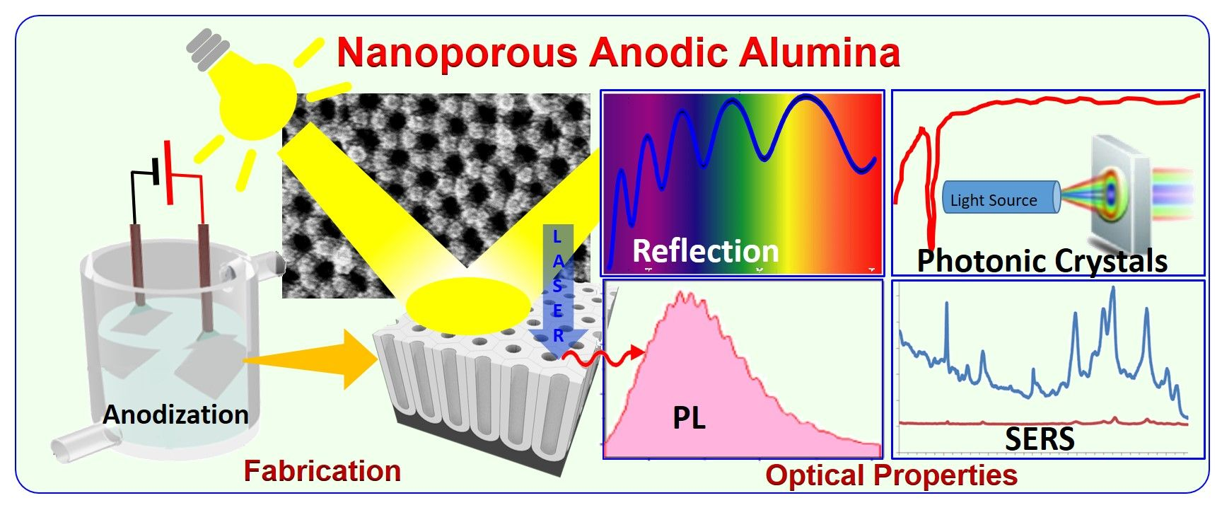
Recent Progress in the Fabrication and Optical Properties of Nanoporous Anodic Alumina


Abstract

1. Introduction
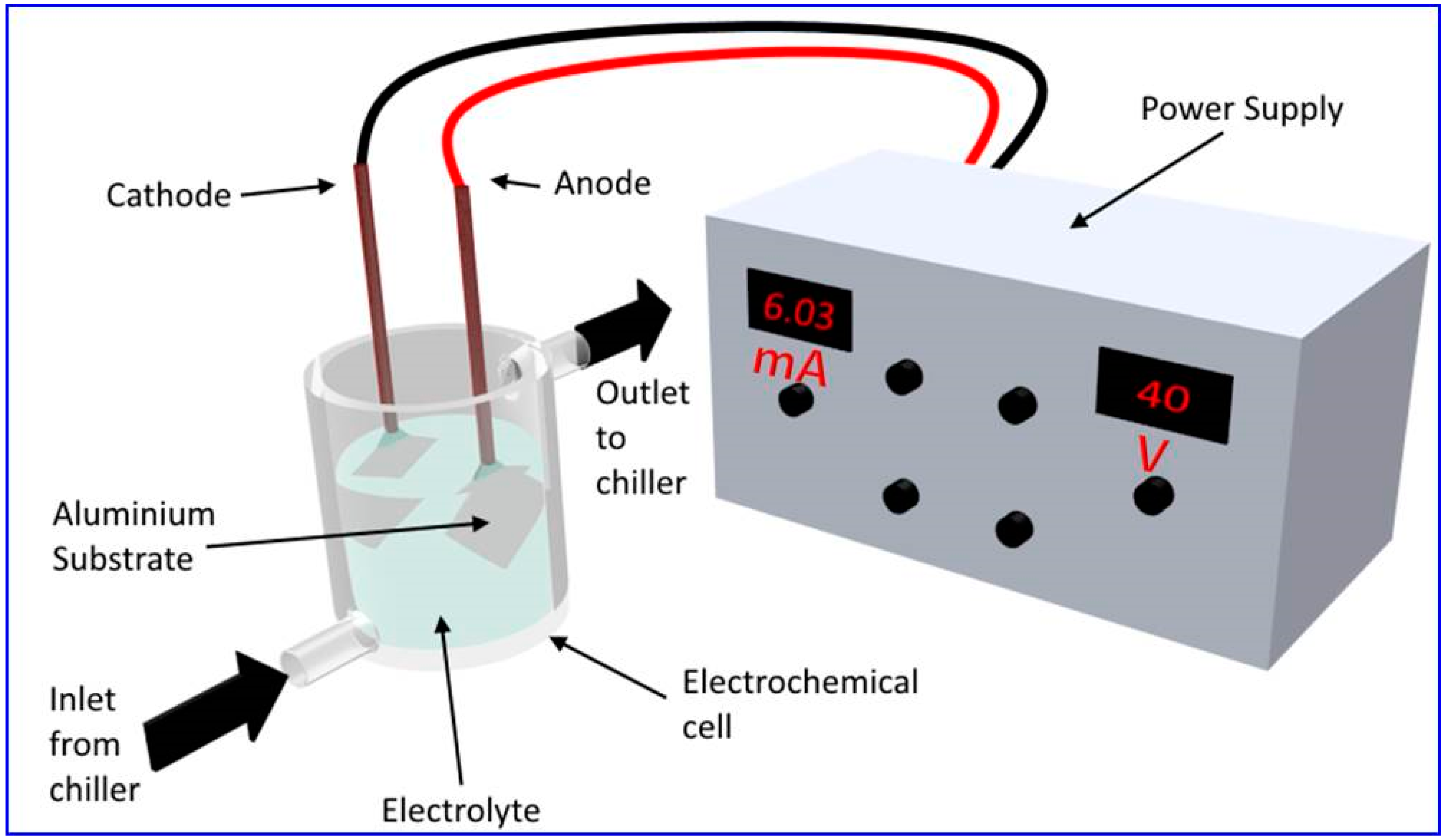
2. Fabrication of Nanoporous Anodic Alumina (NAA) and General Characteristics
- Anodization of aluminum leads to two different morphologies including nonporous barrier alumina and nanoporous alumina;
- Hard anodization resorts to NAA fabrication at potentials higher than the breakdown voltages to obtain thick oxide films in a short time;
- Mild anodization is carried out at much lower voltages to obtain highly ordered nanopore arrays in the most popular electrolytes, namely, sulfuric, oxalic, and phosphoric acids;
- The structural parameters of NAA are dependent on the anodization process parameters, namely, the type and pH of electrolyte, applied anodization potential, current density, and temperature;
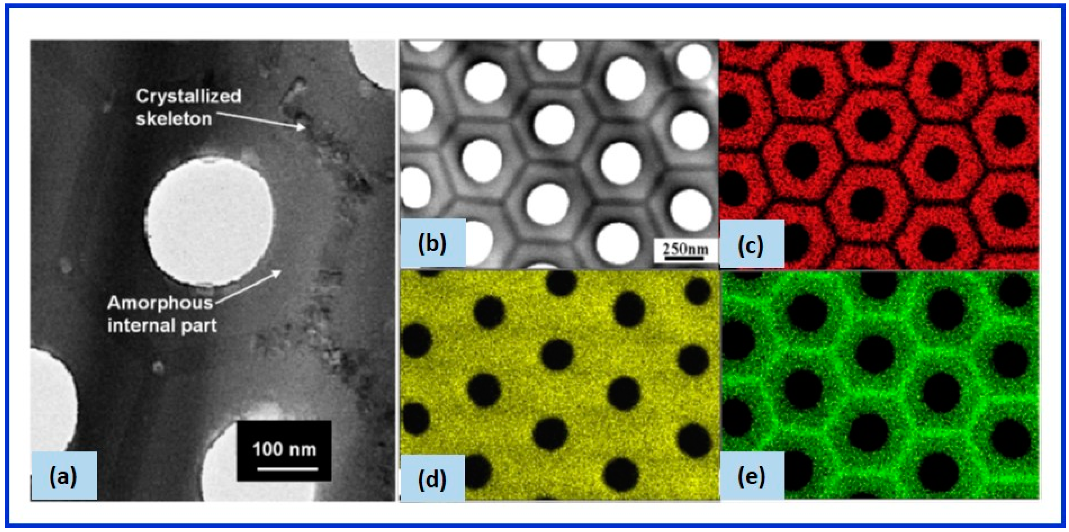
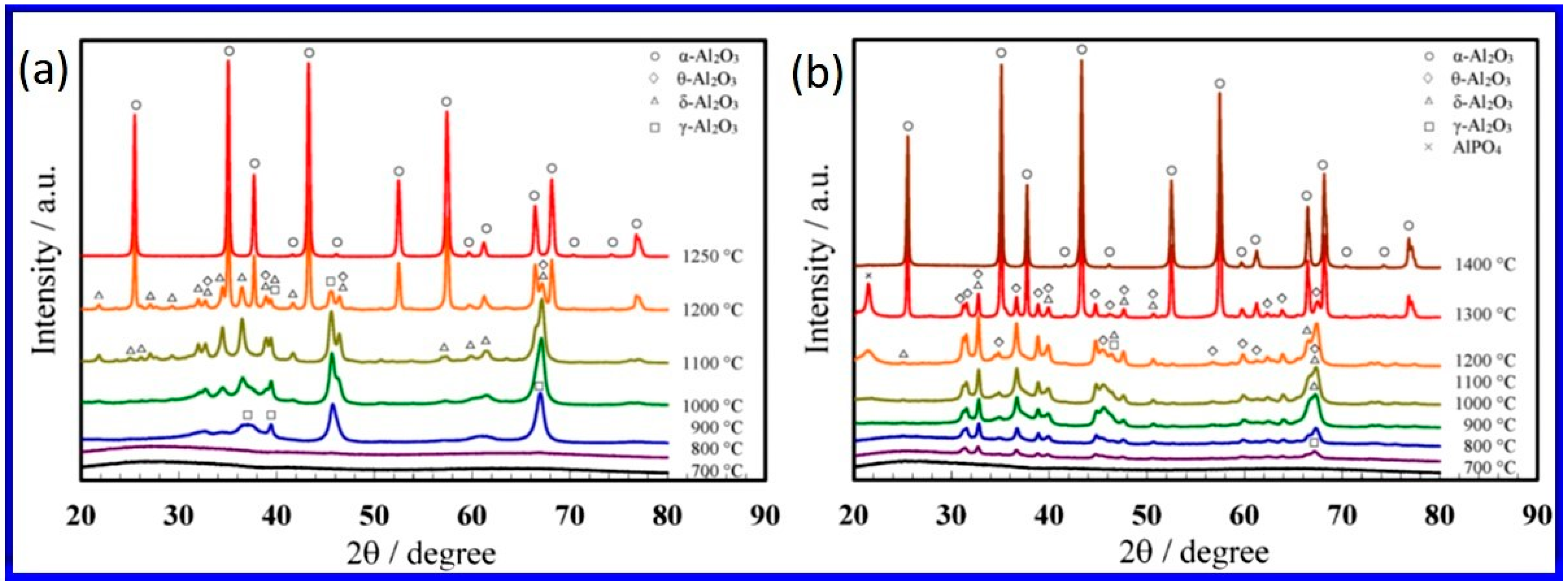
- Chemical resistivity and thermal stability of NAA can be extraordinarily improved by carrying out annealing at high temperatures up to 1500 °C. The annealing makes NAA useful for many practical applications that require exposure to a harsh environment, including corrosive chemical attack and high temperatures;
- Self-ordered NAA with perfectly hexagonally arranged close-packed nanopore arrays can be obtained by two-step anodization process.
2.1. Types of Anodic Alumina Films
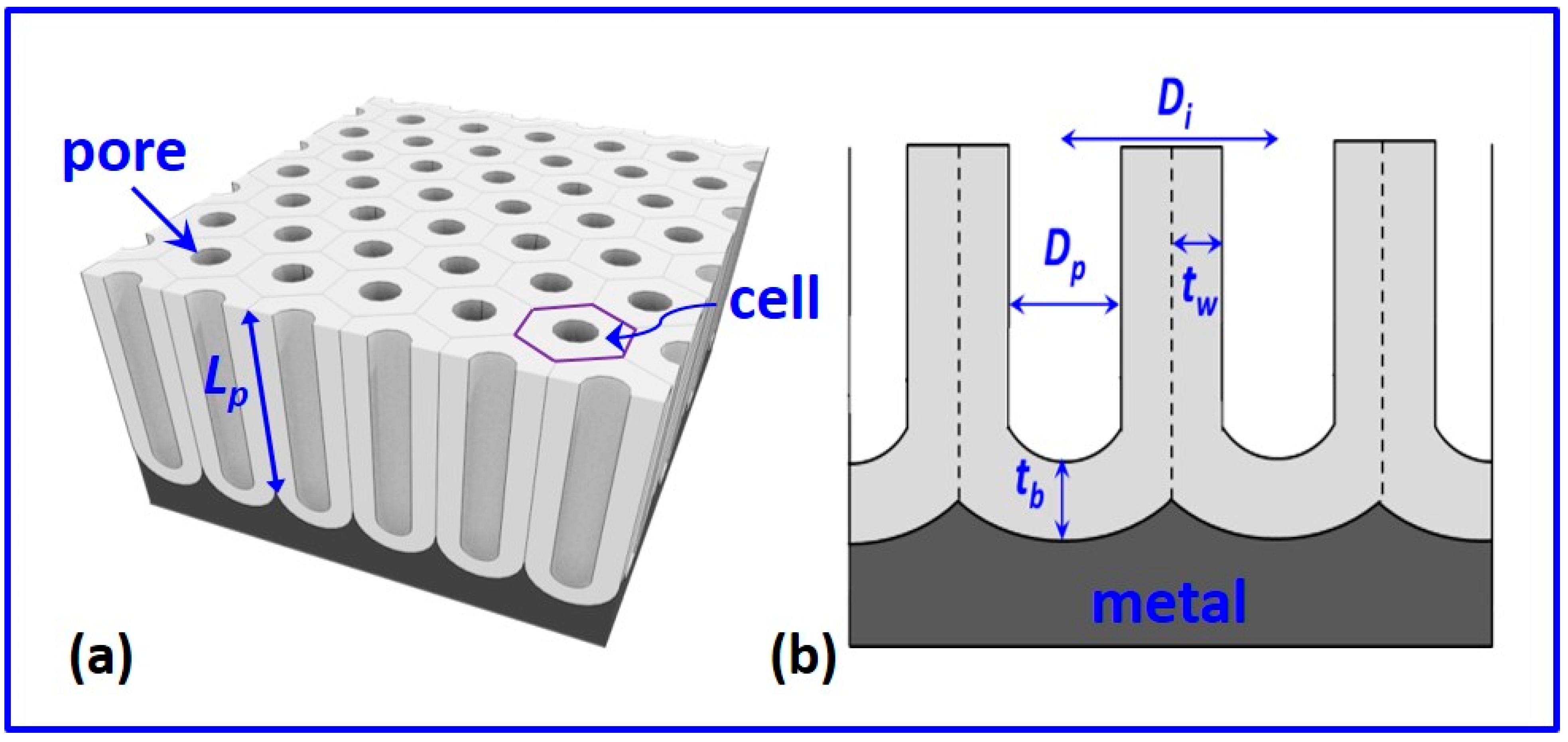
2.2. Structure of NAA
2.2.1. Pore Diameter
2.2.2. Interpore Distance
2.2.3. Pore Wall and Barrier Layer Thickness
2.2.4. Porosity
2.2.5. Effect of Heat Treatment
2.3. Growth and Self-Ordering of NAA
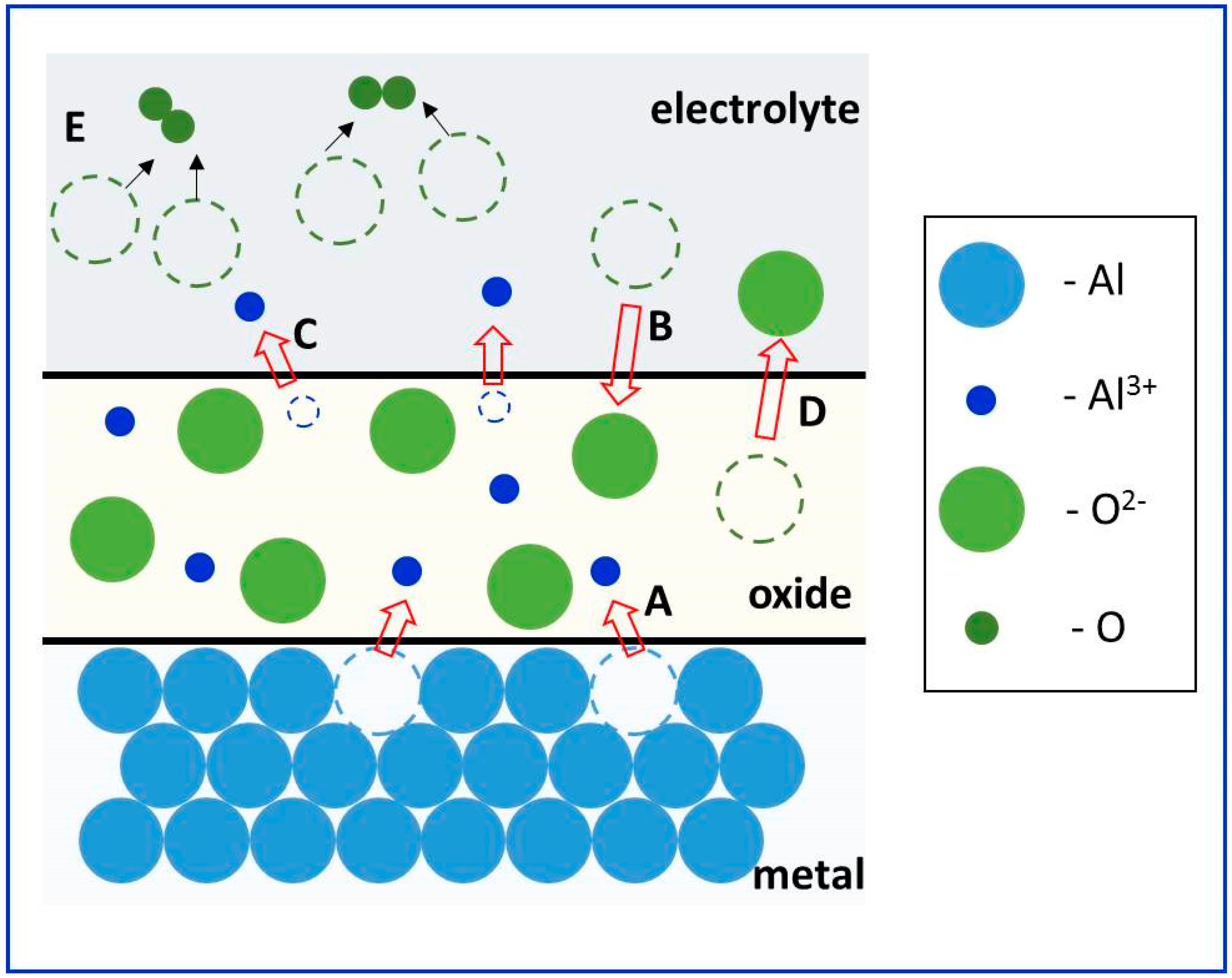
2.3.1. Elementary Reactions in Anodization
- (a)
- At the metal/oxide interface:
- (b)
- At the oxide/electrolyte interface:
2.3.2. Physical Properties of the Oxide—Density, Charge, and Volume Expansion
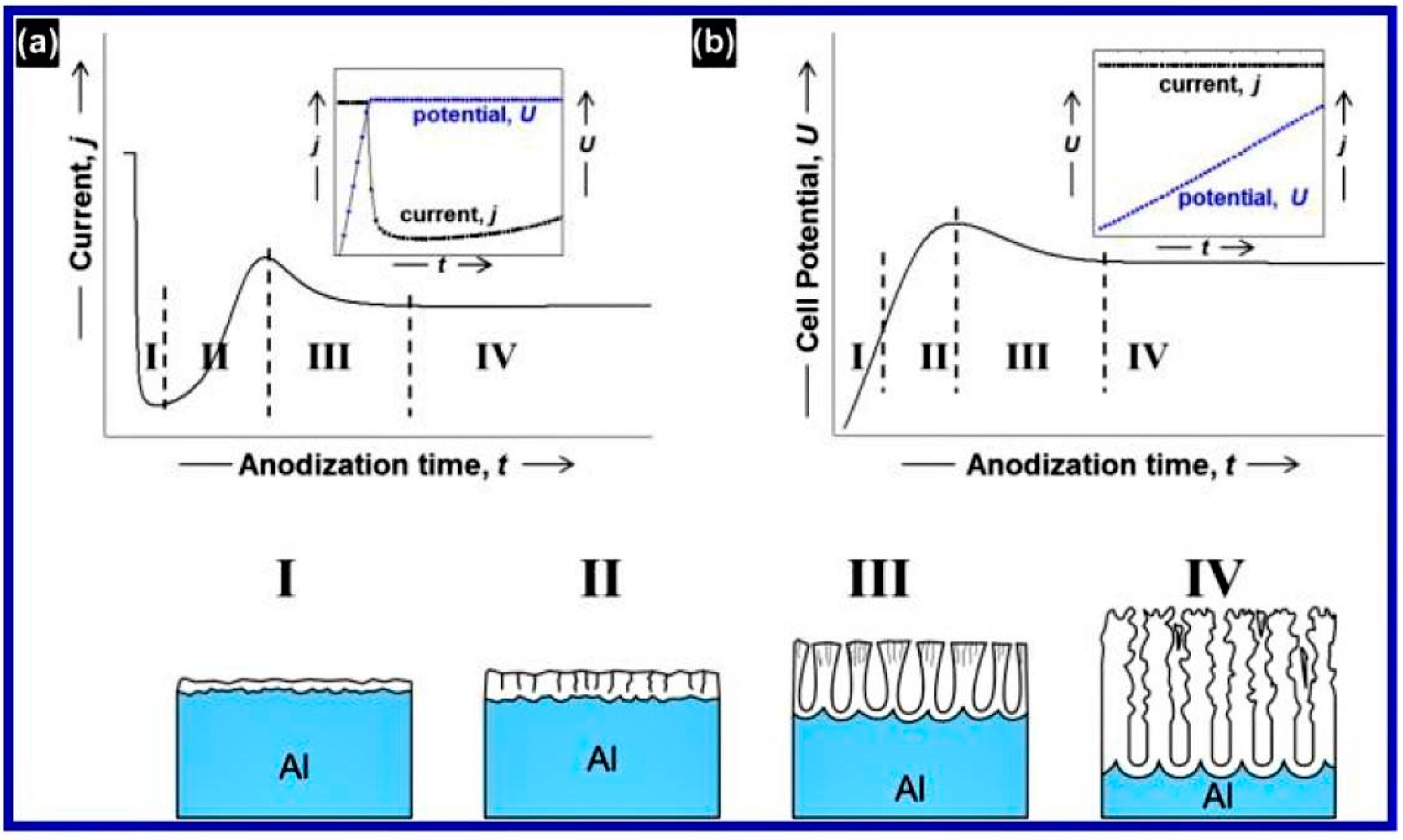
2.3.3. Initial Pore Formation
2.3.4. Kinetics of Porous Oxide Growth
2.3.5. Internal Stress
2.3.6. Self-Ordering of NAA
3. Optical Properties of NAA
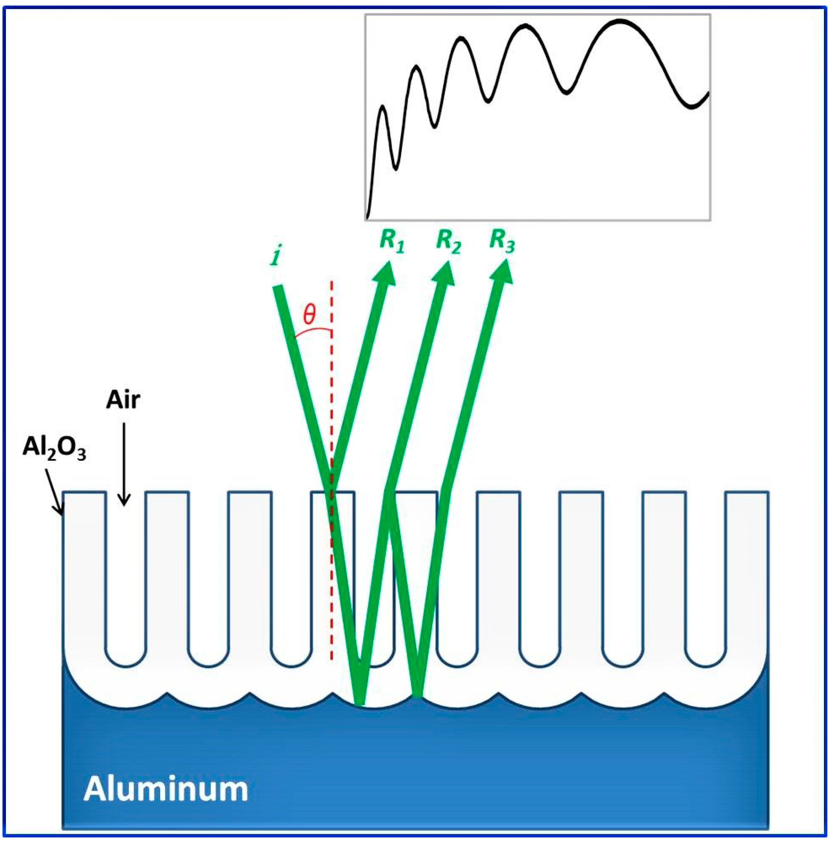
- The optical properties of NAA are governed by the pore properties, namely, pore diameter, pitch, porosity, and pore density, being much different from those of the bulk alumina;
- Reflections from NAA contain oscillations which can be explained using Fabry-Perot interference and used for the optical characterization such as refractive index and pore lengths;
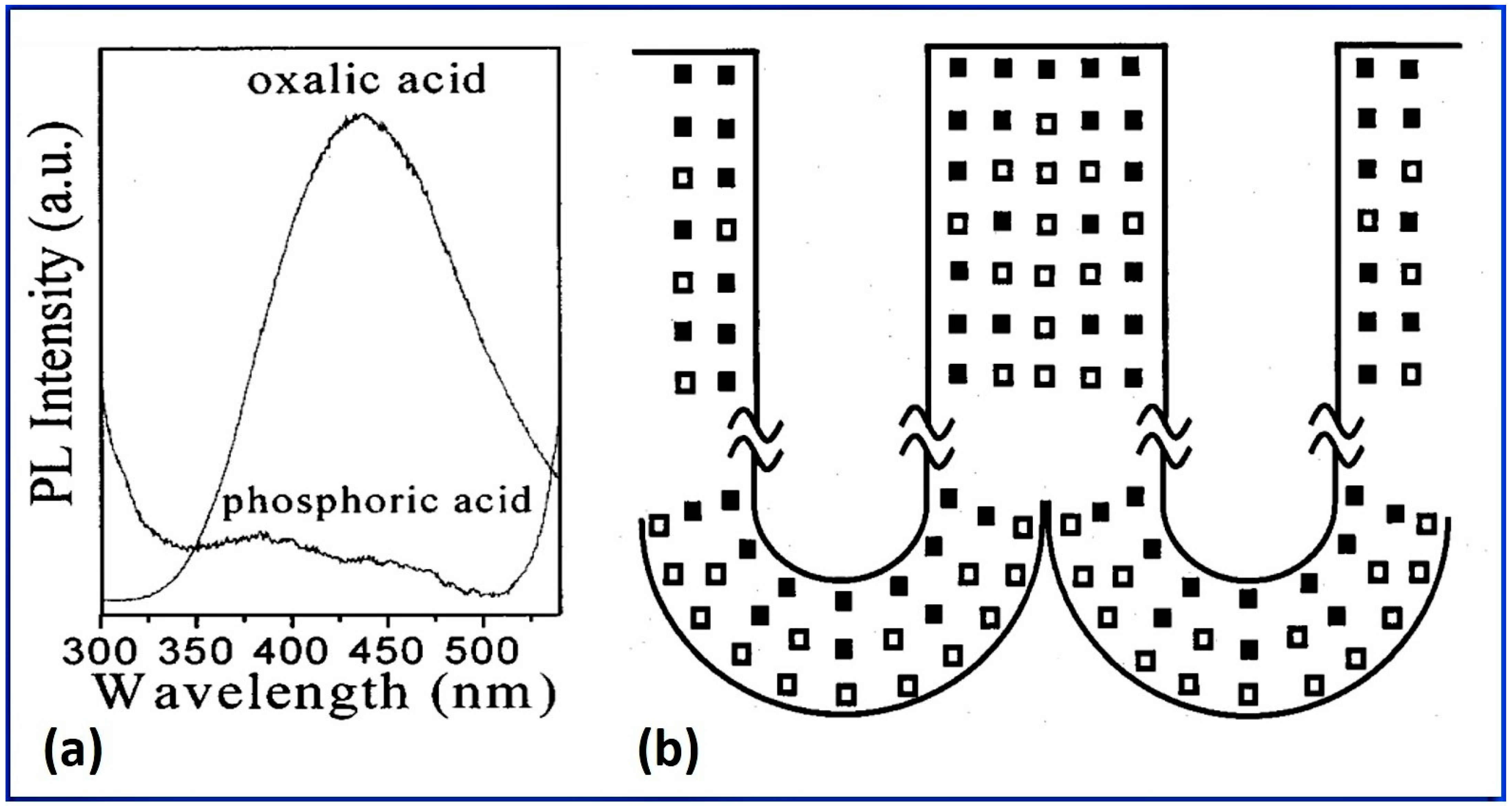
- NAA shows intrinsic blue PL, due to anionic impurities and defect centers, which depends characteristically on the nature and composition of the electrolyte, pore etching treatments, and high-temperature annealing;
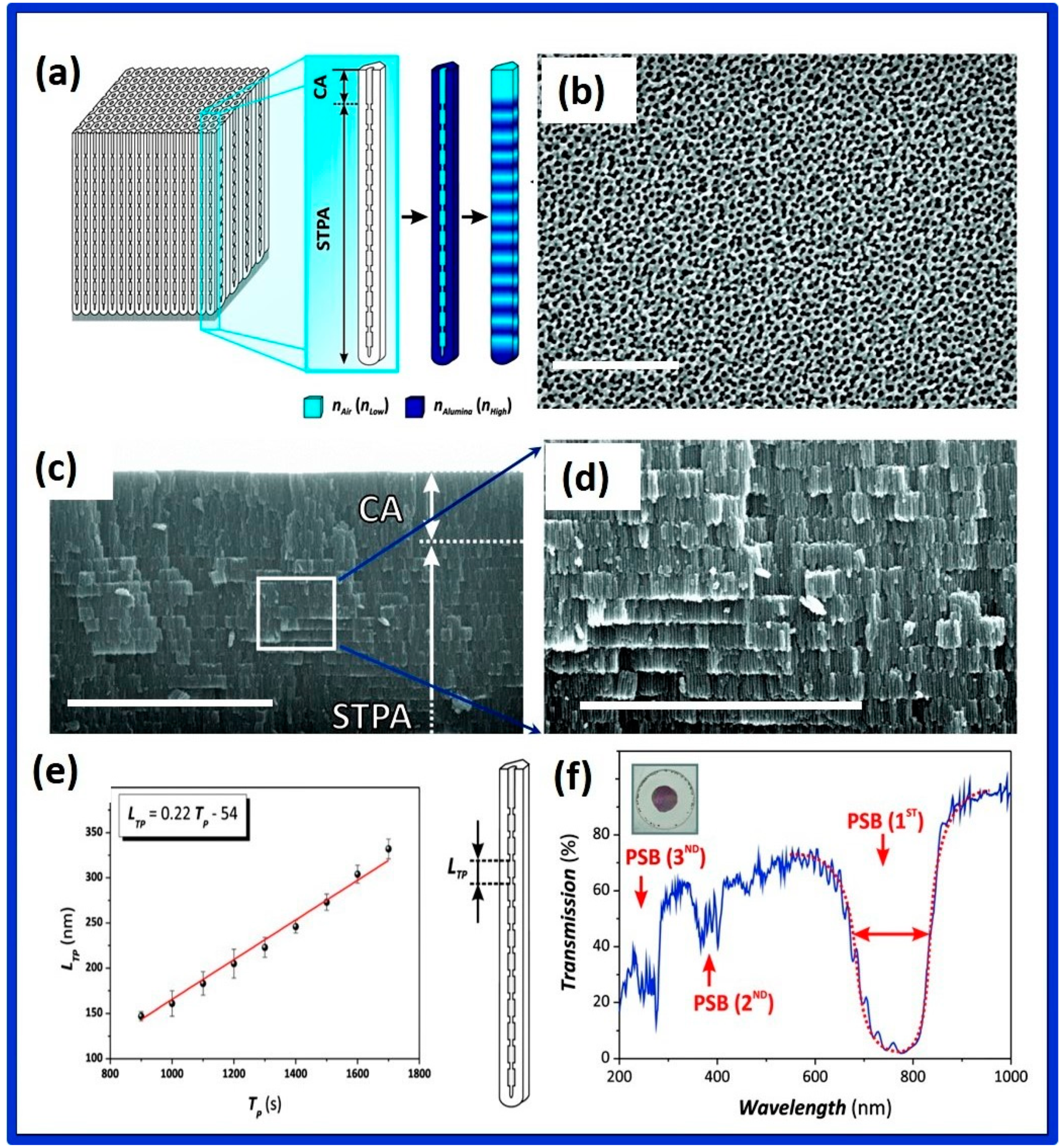
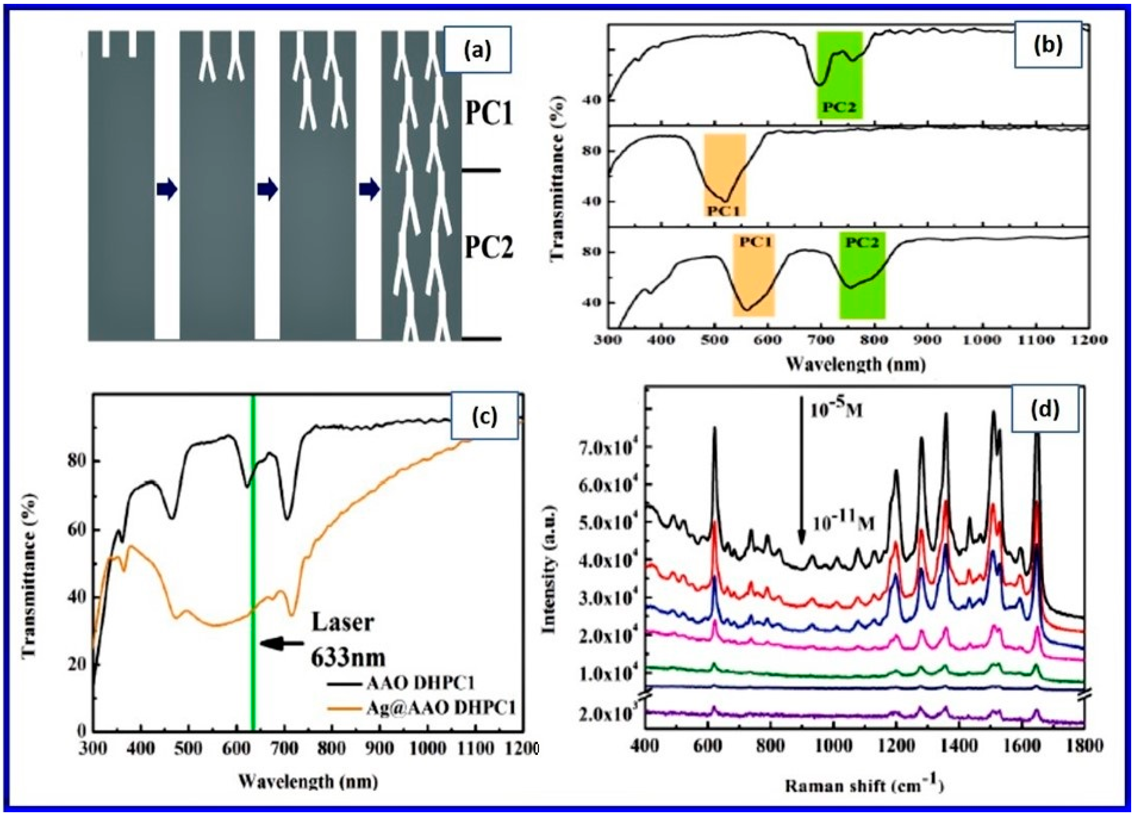
- The ease of production of well-arranged and highly-ordered, perfect geometrical nanopore arrays in the NAA has opened a new pathway for interesting structure related photonic applications, for example, fabrication of photonic crystals and their use in communication and sensing applications;
- Structural and optical engineering of NAA based photonic crystals enabled versatile sensing with enhanced sensitivity, specificity, and selectivity in surface enhanced spectroscopies, specific photonic absorption, and solar anti-reflection properties.
3.1. NAA as a Host Material
3.1.1. Reflection and Transmission in NAA
3.1.2. Absorption in NAA
3.2. Luminescence from NAA
3.2.1. Electroluminescence
3.2.2. Photoluminescence (PL)
Color Centers
Tunability of PL
3.3. Optical Applications of NAA
3.3.1. Direct Use of NAA as a Structural Material
3.3.2. NAA as a Template
4. Summary and Perspectives
Author Contributions
Funding
Data Availability Statement
Conflicts of Interest
References
- Cabrera, N.; Mott, N.F. Theory of the oxidation of metals. Rep. Prog. Phys. 1949, 12, 163. [Google Scholar] [CrossRef]
- Fehlner, F.P.; Mott, N.F. Low-temperature oxidation. Oxid. Met. 1970, 2, 59–99. [Google Scholar] [CrossRef]
- Buff, H. Ueber das electrische Verhalten des Aluminiums. Justus Liebigs Ann. Chem. 1857, 102, 265–284. [Google Scholar] [CrossRef]
- Lee, W.; Park, S.-J. Porous anodic aluminum oxide: Anodization and templated synthesis of functional nanostructures. Chem. Rev. 2014, 114, 7487–7556. [Google Scholar] [CrossRef] [PubMed]
- Masuda, H.; Fukuda, K. Ordered metal nanohole arrays made by a two-step replication of honeycomb structures of anodic alumina. Science 1995, 268, 1466–1468. [Google Scholar] [CrossRef] [PubMed]
- Masuda, H.; Satoh, M. Fabrication of gold nanodot array using anodic porous alumina as an evaporation mask. Jpn. J. Appl. Phys. 1996, 35, L126. [Google Scholar] [CrossRef]
- Santos, A. Nanoporous anodic alumina photonic crystals: Fundamentals, developments and perspectives. J. Mater. Chem. C 2017, 5, 5581–5599. [Google Scholar] [CrossRef]
- Santos, A.; Law, C.S.; Pereira, T.; Losic, D. Nanoporous hard data: Optical encoding of information within nanoporous anodic alumina photonic crystals. Nanoscale 2016, 8, 8091–8100. [Google Scholar] [CrossRef]
- Nielsch, K.; Wehrspohn, R.; Barthel, J.; Kirschner, J.; Gösele, U.; Fischer, S.; Kronmüller, H. Hexagonally ordered 100 nm period nickel nanowire arrays. Appl. Phys. Lett. 2001, 79, 1360–1362. [Google Scholar] [CrossRef]
- Karmhag, R.; Tesfamichael, T.; Wäckelgård, E.; Niklasson, G.A.; Nygren, M. Oxidation Kinetics of Nickel Particles: Comparison between Free Particles and Particles in an Oxide Matrix. Sol. Energy 2000, 68, 329–333. [Google Scholar] [CrossRef]
- Sousa, C.; Leitao, D.; Proenca, M.; Ventura, J.; Pereira, A.; Araujo, J. Nanoporous alumina as templates for multifunctional applications. Appl. Phys. Rev. 2014, 1, 031102. [Google Scholar] [CrossRef]
- Kumeria, T.; Rahman, M.M.; Santos, A.; Ferré-Borrull, J.; Marsal, L.F.; Losic, D. Structural and optical nanoengineering of nanoporous anodic alumina rugate filters for real-time and label-free biosensing applications. Anal. Chem. 2014, 86, 1837–1844. [Google Scholar] [CrossRef] [PubMed]
- Macias, G.; Hernández-Eguía, L.P.; Ferreé-Borrull, J.; Pallares, J.; Marsal, L.F. Gold-coated ordered nanoporous anodic alumina bilayers for future label-free interferometric biosensors. ACS Appl. Mater. Interfaces 2013, 5, 8093–8098. [Google Scholar] [CrossRef] [PubMed]
- Hernández-Eguía, L.P.; Ferré-Borrull, J.; Macias, G.; Pallarès, J.; Marsal, L.F. Engineering optical properties of gold-coated nanoporous anodic alumina for biosensing. Nanoscale Res. Lett. 2014, 9, 414. [Google Scholar] [CrossRef]
- Masuda, H.; Yasui, K.; Nishio, K. Fabrication of ordered arrays of multiple nanodots using anodic porous alumina as an evaporation mask. Adv. Mater. 2000, 12, 1031–1033. [Google Scholar] [CrossRef]
- Che, G.; Lakshmi, B.B.; Martin, C.R.; Fisher, E.R.; Ruoff, R.S. Chemical Vapor Deposition Based Synthesis of Carbon Nanotubes and Nanofibers Using a Template Method. Chem. Mater. 1998, 10, 260–267. [Google Scholar] [CrossRef]
- Zhang, Q.; Xu, J.; Fan, F.; Sun, D.; Xu, G.; Zhang, S.; Zhu, Z. Application of porous anodic alumina monolith catalyst in steam reforming of dimethyl ether: Cu/γ-Al2O3/Al catalyst degradation behaviors and catalytic activity improvement by pre-competition impregnation method. Fuel Processing Technol. 2014, 119, 52–59. [Google Scholar] [CrossRef]
- Gorokh, G.; Mozalev, A.; Solovei, D.; Khatko, V.; Llobet, E.; Correig, X. Anodic formation of low-aspect-ratio porous alumina films for metal-oxide sensor application. Electrochim. Acta 2006, 52, 1771–1780. [Google Scholar] [CrossRef]
- Lu, C.-C.; Huang, Y.-S.; Huang, J.-W.; Chang, C.-K.; Wu, S.-P. A macroporous TiO2 oxygen sensor fabricated using anodic aluminium oxide as an etching mask. Sensors 2010, 10, 670–683. [Google Scholar] [CrossRef]
- Kang, H.-J.; Kim, D.J.; Park, S.-J.; Yoo, J.-B.; Ryu, Y.S. Controlled drug release using nanoporous anodic aluminum oxide on stent. Thin Solid Film. 2007, 515, 5184–5187. [Google Scholar] [CrossRef]
- Sousa, C.T.; Nunes, C.; Proença, M.P.; Leitão, D.C.; Lima, J.L.F.C.; Reis, S.; Araújo, J.P.; Lúcio, M. pH sensitive silica nanotubes as rationally designed vehicles for NSAIDs delivery. Colloids Surf. B Biointerfaces 2012, 94, 288–295. [Google Scholar] [CrossRef] [PubMed]
- Thormann, A.; Teuscher, N.; Pfannmöller, M.; Rothe, U.; Heilmann, A. Nanoporous aluminum oxide membranes for filtration and biofunctionalization. Small 2007, 3, 1032–1040. [Google Scholar] [CrossRef] [PubMed]
- Gaponenko, N.; Orekhovskaya, T.; Nikolaenko, I.; Linnik, O.; Zhukovskii, M.; Smirnova, N.; Prislopskii, S.Y. Titanium oxide xerogel films in porous aluminum oxide for photocatalytic application. J. Appl. Spectrosc. 2010, 77, 432–436. [Google Scholar] [CrossRef]
- Law, C.S.; Santos, A.; Kumeria, T.; Losic, D. Engineered therapeutic-releasing nanoporous anodic alumina-aluminum wires with extended release of therapeutics. ACS Appl. Mater. Interfaces 2015, 7, 3846–3853. [Google Scholar] [CrossRef] [PubMed]
- Fan, Y.; Hotta, K.; Yamaguchi, A.; Ding, Y.; He, Y.; Teramae, N.; Sun, S.; Ma, H. Highly sensitive real-time detection of DNA hybridization by using nanoporous waveguide fluorescence spectroscopy. Appl. Phys. Lett. 2014, 105, 031103. [Google Scholar] [CrossRef]
- Walpole, A.R.; Briggs, E.; Karlsson, M.; Pålsgård, E.; Wilshaw, P. Nano-porous alumina coatings for improved bone implant interfaces. Mater. Werkst. Entwickl. Fert. Prüfung Eig. Anwend. Tech. Werkst. 2003, 34, 1064–1068. [Google Scholar] [CrossRef]
- Jeong, C.; Lee, J.; Sheppard, K.; Choi, C.-H. Air-impregnated nanoporous anodic aluminum oxide layers for enhancing the corrosion resistance of aluminum. Langmuir 2015, 31, 11040–11050. [Google Scholar] [CrossRef]
- Lee, J.; Jiang, Y.; Hizal, F.; Ban, G.-H.; Jun, S.; Choi, C.-H. Durable omniphobicity of oil-impregnated anodic aluminum oxide nanostructured surfaces. J. Colloid Interface Sci. 2019, 553, 734–745. [Google Scholar] [CrossRef]
- Lee, J.; Shin, S.; Jiang, Y.; Jeong, C.; Stone, H.A.; Choi, C.H. Oil-Impregnated Nanoporous Oxide Layer for Corrosion Protection with Self-Healing. Adv. Funct. Mater. 2017, 27, 1606040. [Google Scholar] [CrossRef]
- Ban, G.-H.; Lee, J.; Choi, C.-H.; Li, Y.; Jun, S. Nano-patterned aluminum surface with oil-impregnation for improved antibacterial performance. LWT 2017, 84, 359–363. [Google Scholar] [CrossRef]
- Hizal, F.; Rungraeng, N.; Lee, J.; Jun, S.; Busscher, H.J.; van der Mei, H.C.; Choi, C.-H. Nanoengineered superhydrophobic surfaces of aluminum with extremely low bacterial adhesivity. ACS Appl. Mater. Interfaces 2017, 9, 12118–12129. [Google Scholar] [CrossRef] [PubMed]
- Lee, J.; Kim, D.; Choi, C.-H.; Chung, W. Nanoporous anodic alumina oxide layer and its sealing for the enhancement of radiative heat dissipation of aluminum alloy. Nano Energy 2017, 31, 504–513. [Google Scholar] [CrossRef]
- Thompson, G. Porous anodic alumina: Fabrication, characterization and applications. Thin Solid Film. 1997, 297, 192–201. [Google Scholar] [CrossRef]
- Despić, A.; Parkhutik, V.P. Electrochemistry of Aluminum in Aqueous Solutions and Physics of Its Anodic Oxide. In Modern Aspects of Electrochemistry No. 20; Bockris, J.O.M., White, R.E., Conway, B.E., Eds.; Springer: Boston, MA, USA, 1989; pp. 401–503. [Google Scholar]
- Sulka, G.; Stroobants, S.; Moshchalkov, V.; Borghs, G.; Celis, J.-P. Synthesis of well-ordered nanopores by anodizing aluminum foils in sulfuric acid. J. Electrochem. Soc. 2002, 149, D97–D103. [Google Scholar] [CrossRef]
- Schwirn, K.; Lee, W.; Hillebrand, R.; Steinhart, M.; Nielsch, K.; Gösele, U. Self-Ordered Anodic Aluminum Oxide Formed by H2SO4 Hard Anodization. ACS Nano 2008, 2, 302–310. [Google Scholar] [CrossRef]
- Choudhari, K.; Sudheendra, P.; Udayashankar, N. Fabrication and high-temperature structural characterization study of porous anodic alumina membranes. J. Porous Mater. 2012, 19, 1053–1062. [Google Scholar] [CrossRef]
- Choudhari, K.S.; Kulkarni, S.D.; Santhosh, C.; George, S.D. Photoluminescence enhancement and morphological properties of nanoporous anodic alumina prepared in oxalic acid with varying time and temperature. Microporous Mesoporous Mater. 2018, 271, 138–145. [Google Scholar] [CrossRef]
- Masuda, H.; Yada, K.; Osaka, A. Self-ordering of cell configuration of anodic porous alumina with large-size pores in phosphoric acid solution. Jpn. J. Appl. Phys. 1998, 37, L1340. [Google Scholar] [CrossRef]
- Akiya, S.; Kikuchi, T.; Natsui, S.; Suzuki, R.O. Optimum exploration for the self-ordering of anodic porous alumina formed via selenic acid anodizing. J. Electrochem. Soc. 2015, 162, E244–E250. [Google Scholar] [CrossRef]
- Nishinaga, O.; Kikuchi, T.; Natsui, S.; Suzuki, R.O. Rapid fabrication of self-ordered porous alumina with 10-/sub-10-nm-scale nanostructures by selenic acid anodizing. Sci. Rep. 2013, 3, 2748. [Google Scholar] [CrossRef]
- Lee, W.; Nielsch, K.; Gösele, U. Self-ordering behavior of nanoporous anodic aluminum oxide (AAO) in malonic acid anodization. Nanotechnology 2007, 18, 475713. [Google Scholar] [CrossRef]
- Kikuchi, T.; Yamamoto, T.; Suzuki, R.O. Growth behavior of anodic porous alumina formed in malic acid solution. Appl. Surf. Sci. 2013, 284, 907–913. [Google Scholar] [CrossRef]
- Akiya, S.; Kikuchi, T.; Natsui, S.; Sakaguchi, N.; Suzuki, R.O. Self-ordered porous alumina fabricated via phosphonic acid anodizing. Electrochim. Acta 2016, 190, 471–479. [Google Scholar] [CrossRef]
- Ma, Y.; Wen, Y.; Li, J.; Lu, J.; Li, Y.; Yang, Y.; Feng, C.; Hao, C.; Zhang, Z.; Hu, J. Pore Nucleation Mechanism of Self-Ordered Alumina with Large Period in Stable Anodization in Citric Acid. J. Electrochem. Soc. 2018, 165, E311–E317. [Google Scholar] [CrossRef]
- Mínguez-Bacho, I.; Scheler, F.; Büttner, P.; Bley, K.; Vogel, N.; Bachmann, J. Ordered nanopore arrays with large interpore distances via one-step anodization. Nanoscale 2018, 10, 8385–8390. [Google Scholar] [CrossRef]
- Sepúlveda, M.; Castaño, J.G.; Echeverría, F. Influence of temperature and time on the fabrication of self-ordering porous alumina by anodizing in etidronic acid. Appl. Surf. Sci. 2018, 454, 210–217. [Google Scholar] [CrossRef]
- Elaish, R.; Curioni, M.; Gowers, K.; Kasuga, A.; Habazaki, H.; Hashimoto, T.; Skeldon, P. Effect of fluorozirconic acid on anodizing of aluminium and AA 2024-T3 alloy in sulphuric and tartaric-sulphuric acids. Surf. Coat. Technol. 2018, 342, 233–243. [Google Scholar] [CrossRef]
- Kikuchi, T.; Nishinaga, O.; Natsui, S.; Suzuki, R.O. Fabrication of self-ordered porous alumina via etidronic acid anodizing and structural color generation from submicrometer-scale dimple array. Electrochim. Acta 2015, 156, 235–243. [Google Scholar] [CrossRef]
- Takenaga, A.; Kikuchi, T.; Natsui, S.; Suzuki, R.O. Exploration for the self-ordering of porous alumina fabricated via anodizing in etidronic acid. Electrochim. Acta 2016, 211, 515–523. [Google Scholar] [CrossRef]
- Nakajima, D.; Kikuchi, T.; Natsui, S.; Suzuki, R.O. Growth behavior of anodic oxide formed by aluminum anodizing in glutaric and its derivative acid electrolytes. Appl. Surf. Sci. 2014, 321, 364–370. [Google Scholar] [CrossRef]
- Takenaga, A.; Kikuchi, T.; Natsui, S.; Suzuki, R.O. Self-ordered aluminum anodizing in phosphonoacetic acid and its structural coloration. ECS Solid State Lett. 2015, 4, P55–P58. [Google Scholar] [CrossRef]
- Diggle, J.W.; Downie, T.C.; Goulding, C. Anodic oxide films on aluminum. Chem. Rev. 1969, 69, 365–405. [Google Scholar] [CrossRef]
- Lohrengel, M.M. Thin anodic oxide layers on aluminium and other valve metals: High field regime. Mater. Sci. Eng. R Rep. 1993, 11, 243–294. [Google Scholar] [CrossRef]
- Alwitt, R.; Vijh, A. Sparking voltages observed on anodization of some valve metals. J. Electrochem. Soc. 1969, 116, 388. [Google Scholar] [CrossRef]
- Lee, W. The anodization of aluminum for nanotechnology applications. JOM 2010, 62, 57–63. [Google Scholar] [CrossRef]
- Jani, A.M.M.; Losic, D.; Voelcker, N.H. Nanoporous anodic aluminium oxide: Advances in surface engineering and emerging applications. Prog. Mater. Sci. 2013, 58, 636–704. [Google Scholar] [CrossRef]
- Vega, V.; García, J.; Montero-Moreno, J.M.; Hernando, B.; Bachmann, J.; Prida, V.M.; Nielsch, K. Unveiling the hard anodization regime of aluminum: Insight into nanopores self-organization and growth mechanism. ACS Appl. Mater. Interfaces 2015, 7, 28682–28692. [Google Scholar] [CrossRef]
- Lee, W.; Kim, J.C.; Gösele, U. Spontaneous current oscillations during hard anodization of aluminum under potentiostatic conditions. Adv. Funct. Mater. 2010, 20, 21–27. [Google Scholar] [CrossRef]
- Sun, C.; Luo, J.; Wu, L.; Zhang, J. Self-ordered anodic alumina with continuously tunable pore intervals from 410 to 530 nm. ACS Appl. Mater. Interfaces 2010, 2, 1299–1302. [Google Scholar] [CrossRef]
- Li, Y.; Ling, Z.; Chen, S.; Wang, J. Fabrication of novel porous anodic alumina membranes by two-step hard anodization. Nanotechnology 2008, 19, 225604. [Google Scholar] [CrossRef]
- Chen, X.; Yu, D.; Cao, L.; Zhu, X.; Song, Y.; Huang, H.; Lu, L.; Chen, X. Fabrication of ordered porous anodic alumina with ultra-large interpore distances using ultrahigh voltages. Mater. Res. Bull. 2014, 57, 116–120. [Google Scholar] [CrossRef]
- Lee, W.; Ji, R.; Gösele, U.; Nielsch, K. Fast fabrication of long-range ordered porous alumina membranes by hard anodization. Nat. Mater. 2006, 5, 741–747. [Google Scholar] [CrossRef] [PubMed]
- Choi, J.; Wehrspohn, R.B.; Gösele, U. Mechanism of guided self-organization producing quasi-monodomain porous alumina. Electrochim. Acta 2005, 50, 2591–2595. [Google Scholar] [CrossRef]
- Masuda, H.; Hasegwa, F.; Ono, S. Self-ordering of cell arrangement of anodic porous alumina formed in sulfuric acid solution. J. Electrochem. Soc. 1997, 144, L127. [Google Scholar] [CrossRef]
- Schneider, J.J.; Engstler, J.; Budna, K.P.; Teichert, C.; Franzka, S. Freestanding, Highly Flexible, Large Area, Nanoporous Alumina Membranes with Complete through-Hole Pore Morphology. Eur. J. Inorg. Chem. 2005, 2005, 2352–2359. [Google Scholar] [CrossRef]
- Vrublevsky, I.; Parkoun, V.; Schreckenbach, J. Analysis of porous oxide film growth on aluminum in phosphoric acid using re-anodizing technique. Appl. Surf. Sci. 2005, 242, 333–338. [Google Scholar] [CrossRef]
- Choudhari, K.S.; Jidesh, P.; Sudheendra, P.; Kulkarni, S.D. Quantification and morphology studies of nanoporous alumina membranes: A new algorithm for digital image processing. Microsc. Microanal. 2013, 19, 1061–1072. [Google Scholar] [CrossRef]
- Sulka, G.D.; Zaraska, L.; Stepniowski, W.J. Anodic porous alumina as a template for nanofabrication. In Encyclopedia of Nanoscience and Nanotechnology; Scientific Publishers: Valencia, Spain, 2011; Volume 11, pp. 261–349. [Google Scholar]
- O’sullivan, J.; Wood, G. The morphology and mechanism of formation of porous anodic films on aluminium. Proc. R. Soc. Lond. A 1970, 317, 511–543. [Google Scholar]
- Zhao, N.-Q.; Jiang, X.-X.; Shi, C.-S.; Li, J.-J.; Zhao, Z.-G.; Du, X.-W. Effects of anodizing conditions on anodic alumina structure. J. Mater. Sci. 2007, 42, 3878–3882. [Google Scholar] [CrossRef]
- Sulka, G.; Parkoła, K. Temperature influence on well-ordered nanopore structures grown by anodization of aluminium in sulphuric acid. Electrochim. Acta 2007, 52, 1880–1888. [Google Scholar] [CrossRef]
- Sellarajan, B.; Sharma, M.; Ghosh, S.; Nagaraja, H.; Barshilia, H.C.; Chowdhury, P. Effect of electrolyte temperature on the formation of highly ordered nanoporous alumina template. Microporous Mesoporous Mater. 2016, 224, 262–270. [Google Scholar] [CrossRef]
- Kostaras, C.; Dellis, S.; Christoulaki, A.; Anastassopoulos, D.L.; Spiliopoulos, N.; Vradis, A.; Toprakcioglu, C.; Priftis, G.D. Flow through polydisperse pores in an anodic alumina membrane: A new method to measure the mean pore diameter. J. Appl. Phys. 2018, 124, 204307. [Google Scholar] [CrossRef]
- Nielsch, K.; Choi, J.; Schwirn, K.; Wehrspohn, R.B.; Gösele, U. Self-ordering regimes of porous alumina: The 10 porosity rule. Nano Lett. 2002, 2, 677–680. [Google Scholar] [CrossRef]
- Keller, F.; Hunter, M.; Robinson, D. Structural features of oxide coatings on aluminum. J. Electrochem. Soc. 1953, 100, 411–419. [Google Scholar] [CrossRef]
- Ebihara, K. Structure and density of anodic oxide films formed on aluminum in oxalic acid solutions. J. Surf. Finish. Soc. Jpn. 1983, 34, 548–553. [Google Scholar]
- Ebihara, K. Structure and Density of Anodic Oxyde Films Formed on Aluminium in Sulfuric Acid Solutions. 1982. Available online: https://www.jstage.jst.go.jp/article/sfj1950/33/4/33_4_156/_article/-char/ja (accessed on 31 December 2021).
- Hwang, S.-K.; Jeong, S.-H.; Hwang, H.-Y.; Lee, O.-J.; Lee, K.-H. Fabrication of highly ordered pore array in anodic aluminum oxide. Korean J. Chem. Eng. 2002, 19, 467–473. [Google Scholar] [CrossRef]
- Thompson, G.; Wood, G. Porous anodic film formation on aluminium. Nature 1981, 290, 230–232. [Google Scholar] [CrossRef]
- Hoar, T.P.; Mott, N.F. A mechanism for the formation of porous anodic oxide films on aluminium. J. Phys. Chem. Solids 1959, 9, 97–99. [Google Scholar] [CrossRef]
- Roa, J.J.; Gastón-García, B.; García-Lecina, E.; Müller, C. Mechanical properties at nanometric scale of alumina layers formed in sulphuric acid anodizing under burning conditions. Ceram. Int. 2012, 38, 1627–1633. [Google Scholar] [CrossRef]
- Vojkuvka, L.; Santos, A.; Pallarès, J.; Ferré-Borrull, J.; Marsal, L.; Celis, J.-P. On the mechanical properties of nanoporous anodized alumina by nanoindentation and sliding tests. Surf. Coat. Technol. 2012, 206, 2115–2124. [Google Scholar] [CrossRef]
- Chen, W.; Tang, H.; Shi, C.; Deng, J.; Shi, J.; Zhou, Y.; Xia, S.; Wang, Y.; Yin, S. Investigation on the origin of the blue emission in titanium doped sapphire: Is F+ color center the blue emission center? Appl. Phys. Lett. 1995, 67, 317–319. [Google Scholar] [CrossRef]
- Huang, G.; Wu, X.; Mei, Y.; Shao, X.; Siu, G. Strong blue emission from anodic alumina membranes with ordered nanopore array. J. Appl. Phys. 2003, 93, 582–585. [Google Scholar] [CrossRef]
- Thompson, G.; Xu, Y.; Skeldon, P.; Shimizu, K.; Han, S.; Wood, G. Anodic oxidation of aluminium. Philos. Mag. B 1987, 55, 651–667. [Google Scholar] [CrossRef]
- Ono, S.; Ichinose, H.; Masuko, N. The high resolution observation of porous anodic films formed on aluminum in phosphoric acid solution. Corros. Sci. 1992, 33, 841–850. [Google Scholar] [CrossRef]
- Mason, R.B. Factors affecting the formation of anodic oxide coatings in sulfuric acid electrolytes. J. Electrochem. Soc. 1955, 102, 671. [Google Scholar] [CrossRef]
- Han, H.; Park, S.-J.; Jang, J.S.; Ryu, H.; Kim, K.J.; Baik, S.; Lee, W. In situ determination of the pore opening point during wet-chemical etching of the barrier layer of porous anodic aluminum oxide: Nonuniform impurity distribution in anodic oxide. ACS Appl. Mater. Interfaces 2013, 5, 3441–3448. [Google Scholar] [CrossRef]
- Thompson, G.; Furneaux, R.; Wood, G. Electron microscopy of ion beam thinned porous anodic films formed on aluminium. Corros. Sci. 1978, 18, 481–498. [Google Scholar] [CrossRef]
- Ono, S.; Ichinose, H.; Kawaguchi, T.; Masuko, N. The observation of anodic oxide films on aluminum by high resolution electron microscopy. Corros. Sci. 1990, 31, 249–254. [Google Scholar] [CrossRef]
- Le Coz, F.; Arurault, L.; Datas, L. Chemical analysis of a single basic cell of porous anodic aluminium oxide templates. Mater. Charact. 2010, 61, 283–288. [Google Scholar] [CrossRef]
- Jessensky, O.; Müller, F.; Gösele, U. Self-organized formation of hexagonal pore arrays in anodic alumina. Appl. Phys. Lett. 1998, 72, 1173–1175. [Google Scholar] [CrossRef]
- Zaraska, L.; Stępniowski, W.J.; Ciepiela, E.; Sulka, G.D. The effect of anodizing temperature on structural features and hexagonal arrangement of nanopores in alumina synthesized by two-step anodizing in oxalic acid. Thin Solid Film. 2013, 534, 155–161. [Google Scholar] [CrossRef]
- Lillo, M.; Losic, D. Pore opening detection for controlled dissolution of barrier oxide layer and fabrication of nanoporous alumina with through-hole morphology. J. Membr. Sci. 2009, 327, 11–17. [Google Scholar] [CrossRef]
- Sharma, G.; Pishko, M.V.; Grimes, C.A. Fabrication of metallic nanowire arrays by electrodeposition into nanoporous alumina membranes: Effect of barrier layer. J. Mater. Sci. 2007, 42, 4738–4744. [Google Scholar] [CrossRef]
- Furneaux, R.; Rigby, W.; Davidson, A. The formation of controlled-porosity membranes from anodically oxidized aluminium. Nature 1989, 337, 147–149. [Google Scholar] [CrossRef]
- Santos, A.; Vojkuvka, L.; Pallarés, J.; Ferré-Borrull, J.; Marsal, L.F. In situ electrochemical dissolution of the oxide barrier layer of porous anodic alumina fabricated by hard anodization. J. Electroanal. Chem. 2009, 632, 139–142. [Google Scholar] [CrossRef]
- Stępniowski, W.J.; Florkiewicz, W.; Michalska-Domańska, M.; Norek, M.; Czujko, T. A comparative study of electrochemical barrier layer thinning for anodic aluminum oxide grown on technical purity aluminum. J. Electroanal. Chem. 2015, 741, 80–86. [Google Scholar] [CrossRef]
- Sousa, C.; Leitao, D.; Proenca, M.; Apolinario, A.; Correia, J.; Ventura, J.; Araujo, J. Tunning pore filling of anodic alumina templates by accurate control of the bottom barrier layer thickness. Nanotechnology 2011, 22, 315602. [Google Scholar] [CrossRef]
- Yadav, A.; Bobji, M.; Bull, S.J. Controlled Growth of Highly Aligned Cu Nanowires by Pulse Electrodeposition in Nanoporous Alumina. J. Nanosci. Nanotechnol. 2019, 19, 4254–4259. [Google Scholar] [CrossRef]
- Montero-Rama, M.; Viterisi, A.; Eckstein, C.; Ferré-Borrull, J.; Marsal, L. In-situ removal of thick barrier layer in nanoporous anodic alumina by constant current Re-anodization. Surf. Coat. Technol. 2019, 380, 125039. [Google Scholar] [CrossRef]
- Ma, Y.; Li, K.; Zhou, X.; Wu, H.; Zhu, P.; Yang, B.; Liao, Y.; He, S. Effect of Barrier Layer on Corrosion Resistance of Porous-Type Anodic Films Formed on AA2055 Al–Cu–Li Alloy and Pure Aluminum. J. Electrochem. Soc. 2020, 167, 041508. [Google Scholar] [CrossRef]
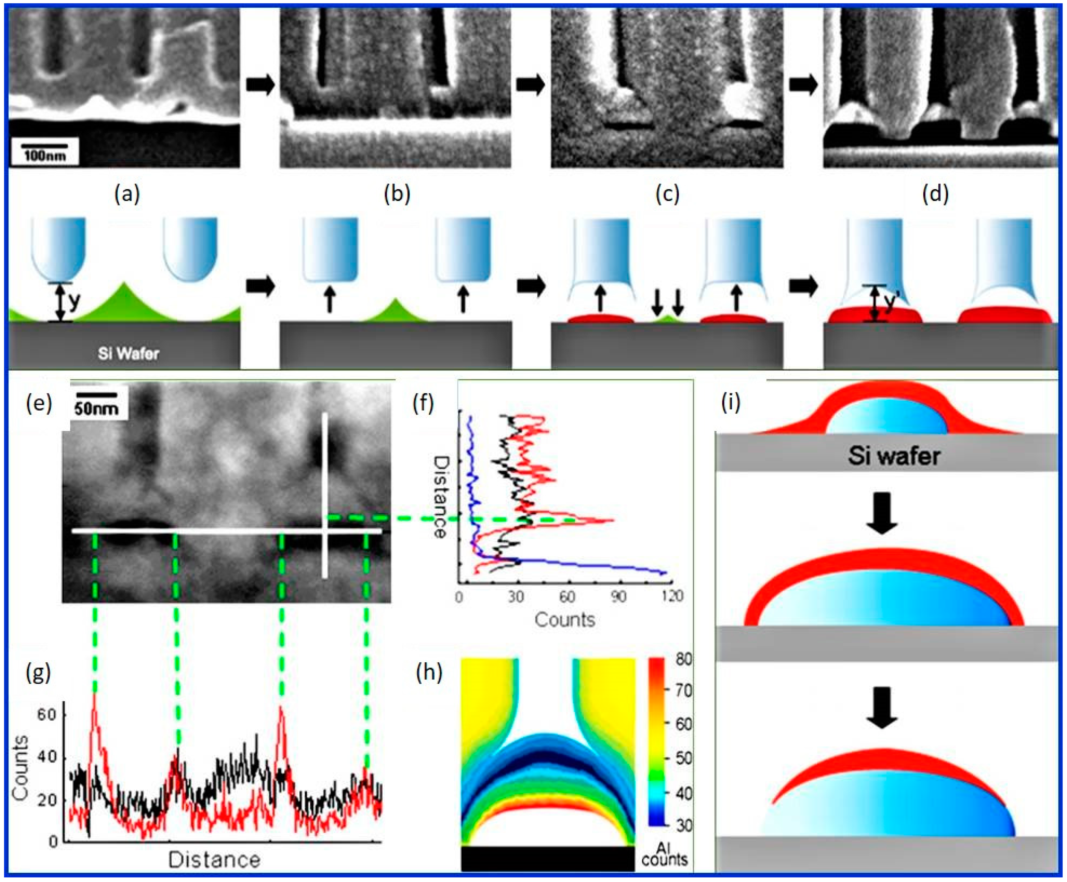
- Seo, H.-S.; Jung, Y.-G.; Jee, S.-W.; Yang, J.M.; Lee, J.-H. Compositionally bilayered feature of interfacial voids in a porous anodic alumina template directly formed on Si. Scr. Mater. 2007, 57, 968–971. [Google Scholar] [CrossRef]
- Chu, S.Z.; Wada, K.; Inoue, S.; Todoroki, S. Formation and microstructures of anodic alumina films from aluminum sputtered on glass substrate. J. Electrochem. Soc. 2002, 149, B321–B327. [Google Scholar] [CrossRef]
- Chu, S.-Z.; Wada, K.; Inoue, S.; Todoroki, S.-I.; Takahashi, Y.K.; Hono, K. Fabrication and characteristics of ordered Ni nanostructures on glass by anodization and direct current electrodeposition. Chem. Mater. 2002, 14, 4595–4602. [Google Scholar] [CrossRef]
- Christoulaki, A.; Chennevière, A.; Dubois, E.; Jouault, N. Duplex nanoporous alumina and polyelectrolyte adsorption: More insights from a combined neutron reflectivity and electron microscopy study. Nanoscale 2019, 11, 2148–2152. [Google Scholar] [CrossRef] [PubMed]
- Crouse, D.; Lo, Y.-H.; Miller, A.E.; Crouse, M. Self-ordered pore structure of anodized aluminum on silicon and pattern transfer. Appl. Phys. Lett. 2000, 76, 49–51. [Google Scholar] [CrossRef]
- Dekker, A.; Middelhoek, A. Transport Numbers and the Structure of Porous Anodic Films on Aluminum. J. Electrochem. Soc. 1970, 117, 440. [Google Scholar] [CrossRef]
- Takahashi, H.; Nagayama, M. The determination of the porosity of anodic oxide films on aluminium by the pore-filling method. Corros. Sci. 1978, 18, 911–925. [Google Scholar] [CrossRef]
- Ono, S.; Saito, M.; Ishiguro, M.; Asoh, H. Controlling factor of self-ordering of anodic porous alumina. J. Electrochem. Soc. 2004, 151, B473–B478. [Google Scholar] [CrossRef]
- Ono, S.; Saito, M.; Asoh, H. Self-Ordering of Anodic Porous Alumina Induced by Local Current Concentration: Burning. Electrochem. Solid-State Lett. 2004, 7, B21. [Google Scholar] [CrossRef]
- Kikuchi, T.; Nishinaga, O.; Natsui, S.; Suzuki, R.O. Self-Ordering Behavior of Anodic Porous Alumina via Selenic Acid Anodizing. Electrochim. Acta 2014, 137, 728–735. [Google Scholar] [CrossRef]
- Chen, W.; Wu, J.-S.; Xia, X.-H. Porous Anodic Alumina with Continuously Manipulated Pore/Cell Size. ACS Nano 2008, 2, 959–965. [Google Scholar] [CrossRef] [PubMed]
- Martín, J.; Manzano, C.V.; Caballero-Calero, O.; Martín-González, M. High-aspect-ratio and highly ordered 15-nm porous alumina templates. ACS Appl. Mater. Interfaces 2013, 5, 72–79. [Google Scholar] [CrossRef] [PubMed]
- Su, Z.; Zhou, W. Formation mechanism of porous anodic aluminium and titanium oxides. Adv. Mater. 2008, 20, 3663–3667. [Google Scholar] [CrossRef]
- Gabe, D.R. Density values for anodic films on aluminium and some observations of pore morphology. Trans. IMF 2000, 78, 207–209. [Google Scholar] [CrossRef]
- Hashimoto, H.; Shigehara, Y.; Ono, S.; Asoh, H. Heat-induced structural transformations of anodic porous alumina formed in phosphoric acid. Microporous Mesoporous Mater. 2018, 265, 77–83. [Google Scholar] [CrossRef]
- Choudhari, K.; Hebbar, D.; Kulkarni, S.D.; Santhosh, C.; George, S.D. Cr3+ doped nanoporous anodic alumina: Facile microwave assisted doping to realize nanoporous ruby and phase dependent photoluminescence. Ceram. Int. 2019, 45, 12130–12137. [Google Scholar] [CrossRef]
- Patra, A.; Tallman, R.; Weinstein, B. Effect of crystal structure and dopant concentration on the luminescence of Cr3+ in Al2O3 nanocrystals. Opt. Mater. 2005, 27, 1396–1401. [Google Scholar] [CrossRef]
- Levin, I.; Brandon, D. Metastable alumina polymorphs: Crystal structures and transition sequences. J. Am. Ceram. Soc. 1998, 81, 1995–2012. [Google Scholar] [CrossRef]
- Brown, I.; Bowden, M.; Kemmitt, T.; MacKenzie, K. Structural and thermal characterisation of nanostructured alumina templates. Curr. Appl. Phys. 2006, 6, 557–561. [Google Scholar] [CrossRef]
- Kirchner, A.; MacKenzie, K.; Brown, I.; Kemmitt, T.; Bowden, M. Structural characterisation of heat-treated anodic alumina membranes prepared using a simplified fabrication process. J. Membr. Sci. 2007, 287, 264–270. [Google Scholar] [CrossRef]
- Mardilovich, P.P.; Govyadinov, A.N.; Mukhurov, N.I.; Rzhevskii, A.M.; Paterson, R. New and modified anodic alumina membranes Part I. Thermotreatment of anodic alumina membranes. J. Membr. Sci. 1995, 98, 131–142. [Google Scholar] [CrossRef]
- Le Coz, F.; Arurault, L.; Fontorbes, S.; Vilar, V.; Datas, L.; Winterton, P. Chemical composition and structural changes of porous templates obtained by anodising aluminium in phosphoric acid electrolyte. Surf. Interface Anal. Int. J. Devoted Dev. Appl. Tech. 2010, 42, 227–233. [Google Scholar] [CrossRef]
- Ozao, R.; Ochiai, M.; Ichimura, N.; Takahashi, H.; Inada, T. DSC study of alumina materials—Applicability of transient DSC (Tr-DSC) to anodic alumina (AA) and thermoanalytical study of AA. Thermochim. Acta 2000, 352, 91–97. [Google Scholar] [CrossRef]
- Bocchetta, P.; Sunseri, C.; Chiavarotti, G.; Di Quarto, F. Microporous alumina membranes electrochemically grown. Electrochim. Acta 2003, 48, 3175–3183. [Google Scholar] [CrossRef]
- Mata-Zamora, M.; Saniger, J. Thermal evolution of porous anodic aluminas: A comparative study. Rev. Mex. Fís. 2005, 51, 502–509. [Google Scholar]
- McQuaig, M.K.; Toro, A.; Van Geertruyden, W.; Misiolek, W.Z. The effect of high temperature heat treatment on the structure and properties of anodic aluminum oxide. J. Mater. Sci. 2011, 46, 243–253. [Google Scholar] [CrossRef]
- Roslyakov, I.V.; Shirin, N.A.; Berekchiian, M.V.; Shatalova, T.B.; Garshev, A.V.; Napolskii, K.S. Coarse-grain alpha-alumina films with highly ordered porous structure. Microporous Mesoporous Mater. 2020, 294, 109840. [Google Scholar] [CrossRef]
- Asoh, H.; Masuda, T.; Ono, S. Nanoporous α-Alumina Membranes with Pore Diameters Tunable over Wide Range of 30–350 nm. ECS Trans. 2015, 69, 225–233. [Google Scholar] [CrossRef]
- Kozhukhova, A.E.; du Preez, S.P.; Bessarabov, D.G. The effects of pore widening and calcination on anodized aluminum oxide prepared from Al6082. Surf. Coat. Technol. 2020, 383, 125234. [Google Scholar] [CrossRef]
- Masuda, T.; Asoh, H.; Haraguchi, S.; Ono, S. Fabrication and characterization of single phase α-alumina membranes with tunable pore diameters. Materials 2015, 8, 1350–1368. [Google Scholar] [CrossRef]
- Fernández-Romero, L.; Montero-Moreno, J.; Pellicer, E.; Peiró, F.; Cornet, A.; Morante, J.; Sarret, M.; Müller, C. Assessment of the thermal stability of anodic alumina membranes at high temperatures. Mater. Chem. Phys. 2008, 111, 542–547. [Google Scholar] [CrossRef]
- Yang, S.; Li, T.; Huang, L.; Tang, T.; Zhang, J.; Gu, B.; Du, Y.; Shi, S.; Lu, Y. Stability of anodic aluminum oxide membranes with nanopores. Phys. Lett. A 2003, 318, 440–444. [Google Scholar] [CrossRef]
- Chang, Y.; Ling, Z.; Liu, Y.; Hu, X.; Li, Y. A simple method for fabrication of highly ordered porous α-alumina ceramic membranes. J. Mater. Chem. 2012, 22, 7445–7448. [Google Scholar] [CrossRef]
- Hashimoto, H.; Kojima, S.; Sasaki, T.; Asoh, H. α-Alumina membrane having a hierarchical structure of straight macropores and mesopores inside the pore wall. J. Eur. Ceram. Soc. 2018, 38, 1836–1840. [Google Scholar] [CrossRef]
- Ono, S.; Nakamura, M.; Masuda, T.; Asoh, H. Fabrication of nanoporous crystalline alumina membrane by anodization of aluminum. Mater. Sci. Forum 2014, 783, 1470–1475. [Google Scholar] [CrossRef]
- Reinhardt, H.M.; Kim, H.-C.; Hampp, N.A. Transformation of anodic aluminum oxide to nanoporous α-Al2O3, ruby and Ti-sapphire micropatterns. J. Eur. Ceram. Soc. 2013, 33, 1281–1287. [Google Scholar] [CrossRef]
- Thompson, G.; Furneaux, R.; Wood, G.; Richardson, J.; Goode, J. Nucleation and growth of porous anodic films on aluminium. Nature 1978, 272, 433–435. [Google Scholar] [CrossRef]
- Davies, J.; Pringle, J.; Graham, R.; Brown, F. A radiotracer study of anodic oxidation. J. Electrochem. Soc. 1962, 109. [Google Scholar] [CrossRef]
- Davies, J.; Domeij, B.; Pringle, J.; Brown, F. The migration of metal and oxygen during anodic film formation. J. Electrochem. Soc. 1965, 112, 675. [Google Scholar] [CrossRef]
- Brown, F.; Mackintosh, W. The use of Rutherford backscattering to study the behavior of ion-implanted atoms during anodic oxidation of Aluminum: Ar, Kr, Xe, K, Rb, Cs, Cl, Br, and l. J. Electrochem. Soc. 1973, 120, 1096. [Google Scholar] [CrossRef]
- Davies, J.; Domeij, B. The use of α-spectroscopy for studying anodic oxidation. J. Electrochem. Soc. 1963, 110, 2425885. [Google Scholar] [CrossRef]
- Paolini, G.; Masoero, M.; Sacchi, F.; Paganelli, M. An investigation of porous anodic oxide films on aluminum by comparative adsorption, gravimetric and electronoptical measurements. J. Electrochem. Soc. 1965, 112, 32. [Google Scholar] [CrossRef]
- Marchal, D.; Demé, B. Small-angle neutron scattering by porous alumina membranes made of aligned cylindrical channels. J. Appl. Crystallogr. 2003, 36, 713–717. [Google Scholar] [CrossRef]
- Liu, Y.; Alwitt, R.; Shimizu, K. Cellular porous anodic alumina grown in neutral organic electrolyte i. Structure, composition, and properties of the films. J. Electrochem. Soc. 2000, 147, 1382. [Google Scholar] [CrossRef]
- Vrublevsky, I.; Parkoun, V.; Schreckenbach, J.; Marx, G. Study of porous oxide film growth on aluminum in oxalic acid using a re-anodizing technique. Appl. Surf. Sci. 2004, 227, 282–292. [Google Scholar] [CrossRef]
- Arurault, L. Pilling–Bedworth ratio of thick anodic aluminium porous films prepared at high voltages in H2SO4 based electrolyte. Trans. IMF 2008, 86, 51–54. [Google Scholar] [CrossRef]
- Li, A.; Müller, F.; Birner, A.; Nielsch, K.; Gösele, U. Hexagonal pore arrays with a 50–420 nm interpore distance formed by self-organization in anodic alumina. J. Appl. Phys. 1998, 84, 6023–6026. [Google Scholar] [CrossRef]
- Parkhutik, V.; Shershulsky, V. Theoretical modelling of porous oxide growth on aluminium. J. Phys. D Appl. Phys. 1992, 25, 1258. [Google Scholar] [CrossRef]
- Shimizu, K.; Kobayashi, K.; Thompson, G.; Wood, G. Development of porous anodic films on aluminium. Philos. Mag. A 1992, 66, 643–652. [Google Scholar] [CrossRef]
- Thamida, S.K.; Chang, H.-C. Nanoscale pore formation dynamics during aluminum anodization. Chaos Interdiscip. J. Nonlinear Sci. 2002, 12, 240–251. [Google Scholar] [CrossRef]
- Bartosik, Ł.; Stafiej, J.; Caprio, D.D. 3D simulations of ordered nanopore growth in alumina. Electrochim. Acta 2016, 188, 218–221. [Google Scholar] [CrossRef]
- Parkhutik, V. The initial stages of aluminium porous anodization studied by Auger electron spectroscopy. Corros. Sci. 1986, 26, 295–310. [Google Scholar] [CrossRef]
- Archibald, L.; Leach, J. The anodic oxidation of zirconium—I. growth stresses in anodic ZrO2 films. Electrochim. Acta 1977, 22, 15–20. [Google Scholar] [CrossRef]
- Bradhurst, D.; Leach, J.L. Discussion of “Stresses in Anodic Films” [DA Vermilyea (pp. 345–346, Vol. 110, No. 4)]. J. Electrochem. Soc. 1963, 110, 1289. [Google Scholar] [CrossRef]
- Vermilyea, D. Stresses in anodic films. J. Electrochem. Soc. (US) Absorbed Electrochem. Technol. 1963, 110. [Google Scholar] [CrossRef]
- Bradhurst, D.; Leach, J.L. The mechanical properties of thin anodic films on aluminum. J. Electrochem. Soc. 1966, 113, 1245–1249. [Google Scholar] [CrossRef]
- Leach, J.L.; Neufeld, P. Mechanical effects during the growth of anodic films. Corros. Sci. 1969, 9, 225–244. [Google Scholar] [CrossRef]
- Moon, S.-M.; Su-II, P. Growth mechanism of anodic oxide films on pure aluminium in aqueous acidic and alkaline solutions. J. Solid State Electrochem. 1998, 2, 156–161. [Google Scholar] [CrossRef]
- Ueno, K.; Seo, M. Stresses of a Titanium Thin-Film Electrode Generated during Anodic Oxidation by a Beam-Bending Method. J. Electrochem. Soc. 2000, 147, 4519. [Google Scholar] [CrossRef]
- Zahavi, J.; Yahalom, J. Temperature increase during formation of anodic films on tantalum. Electrochim. Acta 1971, 16, 89–99. [Google Scholar] [CrossRef]
- Leach, J.; Panagopoulos, C. Temperature rise during anodic oxidation of zirconium. Electrochim. Acta 1985, 30, 1621–1625. [Google Scholar] [CrossRef]
- Nelson, J.; Oriani, R. Stress generation during anodic oxidation of titanium and aluminum. Corros. Sci. 1993, 34, 307–326. [Google Scholar] [CrossRef]
- Ghicov, A.; Schmuki, P. Self-ordering electrochemistry: A review on growth and functionality of TiO2 nanotubes and other self-aligned MOx structures. Chem. Commun. 2009, 20, 2791–2808. [Google Scholar] [CrossRef] [PubMed]
- Ono, S.; Saito, M.; Asoh, H. Self-ordering of anodic porous alumina formed in organic acid electrolytes. Electrochim. Acta 2005, 51, 827–833. [Google Scholar] [CrossRef]
- Singh, G.; Golovin, A.; Aranson, I. Formation of self-organized nanoscale porous structures in anodic aluminum oxide. Phys. Rev. B 2006, 73, 205422. [Google Scholar] [CrossRef]
- Macak, J.M.; Tsuchiya, H.; Taveira, L.; Aldabergerova, S.; Schmuki, P. Smooth anodic TiO2 nanotubes. Angew. Chem. Int. Ed. 2005, 44, 7463–7465. [Google Scholar] [CrossRef]
- Hahn, R.; Macak, J.; Schmuki, P. Rapid anodic growth of TiO2 and WO3 nanotubes in fluoride free electrolytes. Electrochem. Commun. 2007, 9, 947–952. [Google Scholar] [CrossRef]
- Choudhari, K.; Jidesh, P.; Udayashankar, N. Fabrication of nanoporous alumina and their structural characteristics study using SEM image processing and analysis. Synth. React. Inorg. Met.-Org. Nano-Met. Chem. 2012, 42, 369–375. [Google Scholar] [CrossRef]
- Jessensky, O.; Müller, F.; Gösele, U. Self-organized formation of hexagonal pore structures in anodic alumina. J. Electrochem. Soc. 1998, 145, 3735–3740. [Google Scholar] [CrossRef]
- Su, Z.; Hähner, G.; Zhou, W. Investigation of the pore formation in anodic aluminium oxide. J. Mater. Chem. 2008, 18, 5787–5795. [Google Scholar] [CrossRef]
- Yuan, J.; He, F.; Sun, D.; Xia, X. A simple method for preparation of through-hole porous anodic alumina membrane. Chem. Mater. 2004, 16, 1841–1844. [Google Scholar] [CrossRef]
- Moghadam, H.; Samimi, A.; Behzadmehr, A. Solar absorptivity of nano-porous anodic alumina (NPAA): Effects of structural features. J. Porous Mater. 2014, 21, 331–336. [Google Scholar] [CrossRef]
- Gong, S.-H.; Stolz, A.; Myeong, G.-H.; Dogheche, E.; Gokarna, A.; Ryu, S.-W.; Decoster, D.; Cho, Y.-H. Effect of varying pore size of AAO films on refractive index and birefringence measured by prism coupling technique. Opt. Lett. 2011, 36, 4272–4274. [Google Scholar] [CrossRef]
- Marsal, L.; Vojkuvka, L.; Ferré-Borrull, J.; Trifonov, T.; Pallarès, J. Optical characterization of self-ordered porous alumina membranes of various thicknesses. Phys. Status Solidi C 2007, 4, 1918–1922. [Google Scholar] [CrossRef]
- Marthe, J.; Meillot, E.; Jeandel, G.; Enguehard, F.; Ilavsky, J. Enhancement of scattering and reflectance properties of plasma-sprayed alumina coatings by controlling the porosity. Surf. Coat. Technol. 2013, 220, 80–84. [Google Scholar] [CrossRef]
- Xu, Q.; Yang, Y.; Gu, J.; Li, Z.; Sun, H. Influence of Al substrate on the optical properties of porous anodic alumina films. Mater. Lett. 2012, 74, 137–139. [Google Scholar] [CrossRef]
- Xu, C.; Xue, Q.; Zhong, Y.; Cui, Y.; Ba, L.; Zhao, B.; Gu, N. Photoluminescent blue-shift of organic molecules in nanometre pores. Nanotechnology 2002, 13, 47. [Google Scholar] [CrossRef]
- Sulka, G.D. Highly ordered anodic porous alumina formation by self-organized anodizing. Nanostruct. Mater. Electrochem. 2008, 1, 116. [Google Scholar]
- Nakamura, S.; Saito, M.; Huang, L.-F.; Miyagi, M.; Wada, K. Infrared optical constants of anodic alumina films with micropore arrays. Jpn. J. Appl. Phys. 1992, 31, 3589. [Google Scholar] [CrossRef]
- Yakovlev, V.A.; Vinogradov, E.A.; Novikova, N.N.; Mattei, G.; Delplancke-Ogletree, M.P. Infrared reflectivity spectra of thin porous aluminum oxide films. Phys. Status Solidi C 2009, 6, 1697–1699. [Google Scholar] [CrossRef]
- Xu, W.; Chen, H.; Zheng, M.; Ding, G.; Shen, W. Optical transmission spectra of ordered porous alumina membranes with different thicknesses and porosities. Opt. Mater. 2006, 28, 1160–1165. [Google Scholar] [CrossRef]
- Andrushchak, N.; Jaworski, N.; Lobur, M. Improvement of the numerical method for effective refractive index calculation of porous composite materials using microlevel models. Acta Phys. Pol. A 2018, 133, 164–166. [Google Scholar] [CrossRef]
- Hierro-Rodriguez, A.; Rocha-Rodrigues, P.; Valdés-Bango, F.; Alameda, J.; Jorge, P.; Santos, J.L.; Araujo, J.; Teixeira, J.; Guerreiro, A. On the anodic aluminium oxide refractive index of nanoporous templates. J. Phys. D Appl. Phys. 2015, 48, 455105. [Google Scholar] [CrossRef]
- De Laet, J.; Terryn, H.; Vereecken, J. Development of an optical model for steady state porous anodic films on aluminium formed in phosphoric acid. Thin Solid Film. 1998, 320, 241–252. [Google Scholar] [CrossRef]
- De Laet, J.; Vanhellemont, J.; Terryn, H.; Vereecken, J. Characterization of various aluminium oxide layers by means of spectroscopic ellipsometry. Appl. Phys. A 1992, 54, 72–78. [Google Scholar] [CrossRef]
- De Laet, J.; Vanhellemont, J.; Terryn, H.; Vereecken, J. Characterization of different conversion coatings on aluminium with spectroscopic ellipsometry. Thin Solid Film. 1993, 233, 58–62. [Google Scholar] [CrossRef]
- Jung, Y.W.; Byun, J.S.; Woo, D.H.; Kim, Y.D. Ellipsometric analysis of porous anodized aluminum oxide films. Thin Solid Film. 2009, 517, 3726–3730. [Google Scholar] [CrossRef]
- Ferré-Borrull, J.; Pallarès, J.; Macías, G.; Marsal, L.F. Nanostructural Engineering of Nanoporous Anodic Alumina for Biosensing Applications. Materials 2014, 7, 5225. [Google Scholar] [CrossRef]
- Maciulis, V.; Malinovskis, U.; Erts, D.; Ramanavicius, A.; Ramanaviciene, A.; Balevicius, S.; Juciute, S.; Plikusiene, I. Porous aluminium oxide coating for the development of spectroscopic ellipsometry based biosensor: Evaluation of human serum albumin adsorption. Coatings 2020, 10, 1018. [Google Scholar] [CrossRef]
- Xu, Q.; Sun, H.-Y.; Yang, Y.-H.; Liu, L.-H.; Li, Z.-Y. Optical properties and color generation mechanism of porous anodic alumina films. Appl. Surf. Sci. 2011, 258, 1826–1830. [Google Scholar] [CrossRef]
- Wang, X.; Zhang, H.; Zhang, D.; Ma, Y.; Fecht, H.J.; Jiang, J. Color tuning by local sputtering metal nanolayer on microstructured porous alumina. Microsc. Res. Tech. 2012, 75, 698–701. [Google Scholar] [CrossRef] [PubMed]
- Chen, H.M.; Hsin, C.F.; Liu, R.-S.; Hu, S.-F.; Huang, C.-Y. Controlling optical properties of aluminum oxide using electrochemical deposition. J. Electrochem. Soc. 2007, 154, K11–K14. [Google Scholar] [CrossRef]
- Zhang, Y.; Son, S.J.; Ju, H. Anodized aluminum oxide membranes of tunable porosity with platinum nanoscale-coating for photonic application. Curr. Appl. Phys. 2012, 12, 1561–1565. [Google Scholar] [CrossRef]
- Hu, X.; Pu, Y.; Ling, Z.; Li, Y. Coloring of aluminum using photonic crystals of porous alumina with electrodeposited Ag. Opt. Mater. 2009, 32, 382–386. [Google Scholar] [CrossRef]
- Liu, Y.; Wang, H.; Indacochea, J.; Wang, M. A colorimetric sensor based on anodized aluminum oxide (AAO) substrate for the detection of nitroaromatics. Sens. Actuators B Chem. 2011, 160, 1149–1158. [Google Scholar] [CrossRef]
- Jing-Jing, Z.; Zi-Yue, L.; Hui-Min, Z.; Xue, H.; Hui-Yuan, S. Optical and magnetic properties of porous anodic alumina films embedded with Co nanowires. Chin. Phys. B 2013, 22, 087805. [Google Scholar]
- Davoine, F.; Galione, P.; Ramos-Barrado, J.; Leinen, D.; Martín, F.; Dalchiele, E.; Marotti, R. Modeling of gradient index solar selective surfaces for solar thermal applications. Sol. Energy 2013, 91, 316–326. [Google Scholar] [CrossRef]
- Zhang, J.-J.; Li, Z.-Y.; Zhang, Z.-J.; Wu, T.-S.; Sun, H.-Y. Optical and magnetic properties of porous anodic alumina/Ni nanocomposite films. J. Appl. Phys. 2013, 113, 244305. [Google Scholar] [CrossRef]
- Wang, X.; Akahane, T.; Orikasa, H.; Kyotani, T.; Fu, Y. Brilliant and tunable color of carbon-coated thin anodic aluminum oxide films. Appl. Phys. Lett. 2007, 91, 011908. [Google Scholar] [CrossRef]
- Zhao, X.; Meng, G.; Xu, Q.; Han, F.; Huang, Q. Color Fine-Tuning of CNTs@ AAO Composite Thin Films via Isotropically Etching Porous AAO Before CNT Growth and Color Modification by Water Infusion. Adv. Mater. 2010, 22, 2637–2641. [Google Scholar] [CrossRef]
- Wang, B.; Fei, G.T.; Wang, M.; Kong, M.G.; De Zhang, L. Preparation of photonic crystals made of air pores in anodic alumina. Nanotechnology 2007, 18, 365601. [Google Scholar] [CrossRef]
- Kushnir, S.E.; Napolskii, K.S. Thickness-dependent iridescence of one-dimensional photonic crystals based on anodic alumina. Mater. Des. 2018, 144, 140–150. [Google Scholar] [CrossRef]
- Green, S.; Badan, J.; Gilles, M.; Cortes, A.; Riveros, G.; Ramirez, D.; Gómez, H.; Quagliata, E.; Dalchiele, E.; Marotti, R. Optical properties of nanoporous Al2O3 obtained by aluminium anodization. Phys. Status Solidi C 2007, 4, 618–621. [Google Scholar] [CrossRef]
- Markovics, Á.; Nagy, G.; Kovács, B. Reflection-based sensor for gaseous ammonia. Sens. Actuators B Chem. 2009, 139, 252–257. [Google Scholar] [CrossRef]
- Zaghdoudi, W.; Gaidi, M.; Chtourou, R. Microstructural and optical properties of porous alumina elaborated on glass substrate. J. Mater. Eng. Perform. 2013, 22, 869–874. [Google Scholar] [CrossRef]
- Ghrib, M.; Ouertani, R.; Gaidi, M.; Khedher, N.; Salem, M.B.; Ezzaouia, H. Effect of annealing on photoluminescence and optical properties of porous anodic alumina films formed in sulfuric acid for solar energy applications. Appl. Surf. Sci. 2012, 258, 4995–5000. [Google Scholar] [CrossRef]
- Kant, K.; Low, S.P.; Marshal, A.; Shapter, J.G.; Losic, D. Nanopore gradients on porous aluminum oxide generated by nonuniform anodization of aluminum. ACS Appl. Mater. Interfaces 2010, 2, 3447–3454. [Google Scholar] [CrossRef]
- Vrublevsky, I.; Chernyakova, K.; Ispas, A.; Bund, A.; Gaponik, N.; Dubavik, A. Photoluminescence properties of heat-treated porous alumina films formed in oxalic acid. J. Lumin. 2011, 131, 938–942. [Google Scholar] [CrossRef]
- Tsao, Y.-C.; Søndergaard, T.; Skovsen, E.; Gurevich, L.; Pedersen, K.; Pedersen, T.G. Pore size dependence of diffuse light scattering from anodized aluminum solar cell backside reflectors. Opt. Express 2013, 21, A84–A95. [Google Scholar] [CrossRef]
- Choudhari, K.; Kulkarni, S.D.; Unnikrishnan, V.; Sinha, R.K.; Santhosh, C.; George, S.D. Optical characterizations of nanoporous anodic alumina for thickness measurements using interference oscillations. Nano-Struct. Nano-Objects 2019, 19, 100354. [Google Scholar] [CrossRef]
- Fan, D.; Ding, G.; Shen, W.; Zheng, M. Anion impurities in porous alumina membranes: Existence and functionality. Microporous Mesoporous Mater. 2007, 100, 154–159. [Google Scholar] [CrossRef]
- Cantelli, L.; Santos, J.S.; Trivinho-Strixino, F. The effect of anodization temperature on optical properties of nanoporous anodic alumina (NAA) films. J. Electroanal. Chem. 2016, 780, 386–390. [Google Scholar] [CrossRef]
- Gardelis, S.; Nassiopoulou, A.; Gianneta, V.; Theodoropoulou, M. Photoluminescence-induced oscillations in porous anodic aluminum oxide films grown on Si: Effect of the interface and porosity. J. Appl. Phys. 2010, 107, 113104. [Google Scholar] [CrossRef]
- Huang, K.; Pu, L.; Shi, Y.; Han, P.; Zhang, R.; Zheng, Y. Photoluminescence oscillations in porous alumina films. Appl. Phys. Lett. 2006, 89, 201118. [Google Scholar] [CrossRef]
- Choudhari, K.S.; Sangeeth, K.; Kulkarni, S.D.; Chidangil, S. Optical Interferometric Properties of Porous Anodic Alumina Nanostructures. Mater. Today Proc. 2016, 3, 2443–2449. [Google Scholar] [CrossRef]
- Huang, K.; Li, Y.; Wu, Z.; Li, C.; Lai, H.; Kang, J. Asymmetric light reflectance effect in AAO on glass. Opt. Express 2011, 19, 1301–1309. [Google Scholar] [CrossRef]
- Yang, Y.; Gao, Q. Influence of sulfosalicylic acid in the electrolyte on the optical properties of porous anodic alumina membranes. Phys. Lett. A 2004, 333, 328–333. [Google Scholar] [CrossRef]
- Stojadinovic, S.; Nedic, Z.; Belca, I.; Vasilic, R.; Kasalica, B.; Petkovic, M.; Zekovic, L. The effect of annealing on the photoluminescent and optical properties of porous anodic alumina films formed in sulfamic acid. Appl. Surf. Sci. 2009, 256, 763–767. [Google Scholar] [CrossRef]
- Stojadinovic, S.; Belca, I.; Tadic, M.; Kasalica, B.; Nedic, Z.; Zekovic, L. Galvanoluminescence properties of porous oxide films formed by anodization of aluminum in malonic acid. J. Electroanal. Chem. 2008, 619–620, 125–130. [Google Scholar] [CrossRef]
- Guo, P.; Xia, Z.; Xue, Y.; Huang, C.; Zhao, L. Morphology and transmittance of porous alumina on glass substrate. Appl. Surf. Sci. 2011, 257, 3307–3312. [Google Scholar]
- Wang, J.; Wang, C.-W.; Li, Y.; Liu, W.-M. Optical constants of anodic aluminum oxide films formed in oxalic acid solution. Thin Solid Film. 2008, 516, 7689–7694. [Google Scholar] [CrossRef]
- Garabagiu, S.; Mihailescu, G. Thinning anodic aluminum oxide films and investigating their optical properties. Mater. Lett. 2011, 65, 1648–1650. [Google Scholar] [CrossRef]
- Jeon, C.; Kim, D.; Lee, Y.; Han, J.; Choi, Y.; Bu, S.; Shin, H.; Yoon, S. Strong pore-size dependence of the optical properties in porous alumina membranes. J. Korean Phys. Soc. 2013, 63, 1789–1793. [Google Scholar] [CrossRef]
- Liu, Y.-F.; Tu, Y.-F.; Huang, S.-Y.; Sang, J.-P.; Zou, X.-W. Effect of etch-treatment upon the intensity and peak position of photoluminescence spectra for anodic alumina films with ordered nanopore array. J. Mater. Sci. 2009, 44, 3370–3375. [Google Scholar] [CrossRef]
- Lee, K.-W.; Yang, T.-H.; Lu, W.-L.; Houng, M.-P. Fabricating 20 cm × 20 cm porous template using anodic aluminum oxide. Integr. Ferroelectr. 2013, 143, 47–57. [Google Scholar] [CrossRef]
- Efeoglu, H.; Karacali, T.; Meral, K.; Erdog, İ.Y.; Onganer, Y. Anodization of aluminium thin films on p++ Si and annihilation of strong luminescence from Al2O3. J. Lumin. 2010, 130, 157–162. [Google Scholar] [CrossRef]
- Gao, T.; Meng, G.-W.; Zhang, L.-D. Origin of the blue luminescence in porous anodic alumina films formed in oxalic acid solutions. Chin. Phys. Lett. 2003, 20, 713. [Google Scholar]
- Stępniowski, W.J.; Norek, M.; Michalska-Domańska, M.; Bombalska, A.; Nowak-Stępniowska, A.; Kwaśny, M.; Bojar, Z. Fabrication of anodic aluminum oxide with incorporated chromate ions. Appl. Surf. Sci. 2012, 259, 324–330. [Google Scholar] [CrossRef]
- Kurashima, Y.; Yokota, Y.; Miyamoto, I.; Kataura, H.; Sakakibara, Y. Mode-locking nanoporous alumina membrane embedded with carbon nanotube saturable absorber. Appl. Phys. Lett. 2009, 94, 223102. [Google Scholar] [CrossRef]
- Li, Y.; Li, G.; Meng, G.; Zhang, L.; Phillipp, F. Photoluminescence and optical absorption caused by the F+ centres in anodic alumina membranes. J. Phys. Condens. Matter 2001, 13, 2691. [Google Scholar] [CrossRef]
- Gao, T.; Meng, G.; Zhang, L. Blue luminescence in porous anodic alumina films: The role of the oxalic impurities. J. Phys. Condens. Matter 2003, 15, 2071. [Google Scholar] [CrossRef]
- Gao, T.; Meng, G.; Zhang, L. Ultraviolet photoluminescence of porous anodic alumina films. Chin. Sci. Bull. 2003, 48, 1090–1092. [Google Scholar] [CrossRef]
- Li, T.; Yang, S.; Huang, L.; Zhang, J.; Gu, B.; Du, Y. Strong photoluminescence from Cr3+ doped porous anodic alumina. J. Phys. Condens. Matter 2004, 16, 2463. [Google Scholar] [CrossRef]
- Stępniowski, W.J.; Norek, M.; Michalska-Domańska, M.; Nowak-Stępniowska, A.; Bombalska, A.; Włodarski, M.; Bojar, Z. Incorporation of copper chelate ions into anodic alumina walls. Mater. Lett. 2013, 106, 242–245. [Google Scholar] [CrossRef]
- Tajima, S. Luminescence, breakdown and colouring of anodic oxide films on aluminium. Electrochim. Acta 1977, 22, 995–1011. [Google Scholar] [CrossRef]
- Stojadinovic, S.; Vasilic, R.; Belca, I.; Tadic, M.; Kasalica, B.; Zekovic, L. Structural and luminescence characterization of porous anodic oxide films on aluminum formed in sulfamic acid solution. Appl. Surf. Sci. 2008, 255, 2845–2850. [Google Scholar] [CrossRef]
- Braun, F. Ueber lichtenmission an einigen electroden in electrolyten. Ann. Der Phys. 1898, 301, 361–364. [Google Scholar] [CrossRef]
- Belca, I.; Kasalica, B.; Zekovic, L.; Jovanic, B.; Vasilic, R. The galvanoluminescence spectra of porous oxide layers formed by aluminum anodization in oxalic acid. Electrochim. Acta 1999, 45, 993–996. [Google Scholar] [CrossRef]
- Stojadinovic, S.; Zekovic, L.; Belca, I.; Kasalica, B. Galvanoluminescence of oxide films formed by anodization of aluminum in phosphoric acid. Electrochem. Commun. 2004, 6, 427–431. [Google Scholar] [CrossRef]
- Stojadinovic, S.; Zekovic, L.; Belca, I.; Kasalica, B.; Nikolic, D. The influence of anodizing conditions on the galvanoluminescence spectra of porous oxide films on aluminum formed in phosphoric acid solution. Electrochem. Commun. 2004, 6, 708–712. [Google Scholar] [CrossRef]
- Stojadinovic, S.; Belca, I.; Zekovic, L.; Kasalica, B.; Nikolic, D. Galvanoluminescence of porous oxide films formed by anodization of aluminum in chromic acid solution. Electrochem. Commun. 2004, 6, 1016–1020. [Google Scholar] [CrossRef]
- Kasalica, B.; Stojadinovic, S.; Zekovic, L.; Belca, I.; Nikolic, D. The influence of aluminum treatment and anodizing conditions on the galvanoluminescence properties of porous oxide films formed in sulfuric acid solution. Electrochem. Commun. 2005, 7, 735–739. [Google Scholar] [CrossRef]
- Vermilyea, D. Flaws in Anodic Ta2O5 Films. J. Electrochem. Soc. 1963, 110, 250. [Google Scholar] [CrossRef]
- Shimizu, K. Electroluminescence of Al/anodic alumina/electrolyte system and non destructive electronic avalanche. Electrochim. Acta 1978, 23, 295–298. [Google Scholar] [CrossRef]
- Marsland, L.C.; Burstein, G.T. Electroluminescence of aluminium during electropolishing in nitric acid. Electrochem. Commun. 2000, 2, 591–594. [Google Scholar] [CrossRef]
- Haapakka, K.; Kankare, J.; Kulmala, S. Feasibility of low-voltage cathodic electroluminescence at oxide-covered aluminum electrodes for trace metal determinations in aqueous solutions. Anal. Chim. Acta 1985, 171, 259–267. [Google Scholar] [CrossRef]
- Zeković, L.D.; Urošević, V.V. The role of interference in the electroluminescence of thin anodic oxide films. Thin Solid Film. 1981, 78, 279–286. [Google Scholar] [CrossRef]
- Zeković, L.D.; Urošević, V.V. New investigations of the interference effect in electroluminescence of anodic films on aluminum. Thin Solid Film. 1981, 86, 347–350. [Google Scholar] [CrossRef]
- Cantelli, L.; Santos, J.S.; Silva, T.F.; Tabacniks, M.H.; Delgado-Silva, A.O.; Trivinho-Strixino, F. Unveiling the origin of photoluminescence in nanoporous anodic alumina (NAA) obtained by constant current regime. J. Lumin. 2019, 207, 63–69. [Google Scholar] [CrossRef]
- Mukhurov, N.; Zhvavyi, S.; Terekhov, S.; Panarin, A.Y.; Kotova, I.; Pershukevich, P.; Khodasevich, I.; Gasenkova, I.; Orlovich, V. Influence of electrolyte composition on photoluminescent properties of anodic aluminum oxide. J. Appl. Spectrosc. 2008, 75, 214–218. [Google Scholar] [CrossRef]
- Choudhari, K.; Kulkarni, S.D.; Santhosh, C.; George, S.D. Influence of electrolyte composition on the photoluminescence and pore arrangement of nanoporous anodic alumina. ECS J. Solid State Sci. Technol. 2018, 7, R175–R182. [Google Scholar] [CrossRef]
- Li, Y.; Wang, C.-W.; Zhao, L.-R.; Liu, W.-M. Photoluminescence properties of porous anodic aluminium oxide membranes formed in mixture of sulfuric and oxalic acid. J. Phys. D Appl. Phys. 2009, 42, 045407. [Google Scholar] [CrossRef]
- Wang, J.; Wang, C.-W.; Li, S.-Y.; Zhou, F. The effect of oxalic and sulfuric ions on the photoluminescence of anodic aluminum oxide formed in a mixture of sulfuric and oxalic acid. Appl. Phys. A 2009, 94, 939–942. [Google Scholar] [CrossRef]
- Li, S.-Y.; Wang, J.; Li, Y.; Zhang, X.-Q.; Wang, G.; Wang, C.-W. Photoluminescent properties of anodic aluminum oxide films formed in a mixture of malonic and sulfuric acid. Superlattices Microstruct. 2014, 75, 294–302. [Google Scholar] [CrossRef]
- Xu, W.; Zheng, M.; Wu, S.; Shen, W. Effects of high-temperature annealing on structural and optical properties of highly ordered porous alumina membranes. Appl. Phys. Lett. 2004, 85, 4364–4366. [Google Scholar] [CrossRef]
- Li, G.; Zhang, Y.; Wu, Y.; Zhang, L. Wavelength dependent photoluminescence of anodic alumina membranes. J. Phys. Condens. Matter 2003, 15, 8663. [Google Scholar] [CrossRef]
- Du, Y.; Cai, W.; Mo, C.; Chen, J.; Zhang, L.; Zhu, X. Preparation and photoluminescence of alumina membranes with ordered pore arrays. Appl. Phys. Lett. 1999, 74, 2951–2953. [Google Scholar] [CrossRef]
- Nourmohammadi, A.; Asadabadi, S.J.; Yousefi, M.H.; Ghasemzadeh, M. Photoluminescence emission of nanoporous anodic aluminum oxide films prepared in phosphoric acid. Nanoscale Res. Lett. 2012, 7, 689. [Google Scholar] [CrossRef]
- Li, Z.; Huang, K. Blue luminescence in porous anodic alumina films. J. Phys. Condens. Matter 2007, 19, 216203. [Google Scholar] [CrossRef]
- Mukhurov, N.; Zhvavyi, S.; Gasenkova, I.; Terekhov, S.; Pershukevich, P.; Orlovich, V. Photoluminescence of F-centers in films of anodic alumina. J. Appl. Spectrosc. 2010, 77, 549–555. [Google Scholar] [CrossRef]
- Yamamoto, Y.; Baba, N.; Tajima, S. Coloured materials and photoluminescence centres in anodic film on aluminium. Nature 1981, 289, 572–574. [Google Scholar] [CrossRef]
- Wu, J.; Wu, X.; Tang, N.; Mei, Y.; Bao, X. Strong ultraviolet and violet photoluminescence from Si-based anodic porous alumina films. Appl. Phys. A 2001, 72, 735–737. [Google Scholar] [CrossRef]
- Draeger, B.; Summers, G. Defects in unirradiated α-Al2O3. Phys. Rev. B 1979, 19, 1172. [Google Scholar] [CrossRef]
- Huang, G.; Wu, X.; Yang, L.W.; Shao, X.; Siu, G.; Chu, P. Dependence of blue-emitting property on nanopore geometrical structure in Al-based porous anodic alumina membranes. Appl. Phys. A 2005, 81, 1345–1349. [Google Scholar] [CrossRef]
- Siejka, J.; Ortega, C. An O18 study of field-assisted pore formation in compact anodic oxide films on aluminum. J. Electrochem. Soc. 1977, 124, 883–891. [Google Scholar] [CrossRef]
- Cherki, C.; Siejka, J. Study by nuclear microanalysis and O18 tracer techniques of the oxygen transport processes and the growth laws for porous anodic oxide layers on aluminum. J. Electrochem. Soc. 1973, 120, 784–791. [Google Scholar] [CrossRef]
- Gasenkova, I.; Mukhurov, N.; Zhvavyi, S.; Kolesnik, E.; Stupak, A. Photoluminescent properties of nanoporous anodic alumina doped with manganese ions. J. Lumin. 2017, 185, 298–305. [Google Scholar] [CrossRef]
- Khan, G.G.; Singh, A.K.; Mandal, K. Structure dependent photoluminescence of nanoporous amorphous anodic aluminium oxide membranes: Role of F+ center defects. J. Lumin. 2013, 134, 772–777. [Google Scholar] [CrossRef]
- Chen, J.; Huang, C.; Chao, C.; Chen, T.-M. The investigation of photoluminescence centers in porous alumina membranes. Appl. Phys. A 2006, 84, 297–300. [Google Scholar] [CrossRef]
- Li, Z.; Huang, K. Optical properties of alumina membranes prepared by anodic oxidation process. J. Lumin. 2007, 127, 435–440. [Google Scholar] [CrossRef]
- Santos, A.; Law, C.S.; Lei, D.W.C.; Pereira, T.; Losic, D. Fine tuning of optical signals in nanoporous anodic alumina photonic crystals by apodized sinusoidal pulse anodisation. Nanoscale 2016, 8, 18360–18375. [Google Scholar] [CrossRef]
- Vrublevsky, I.; Jagminas, A.; Hemeltjen, S.; Goedel, W.A. Photoluminescent behavior of heat-treated porous alumina films formed in malonic acid. Appl. Surf. Sci. 2010, 256, 2013–2017. [Google Scholar] [CrossRef]
- Vrublevsky, I.; Jagminas, A.; Hemeltjen, S.; Goedel, W. Behavior of acid species during heat treatment and re-anodizing of porous alumina films formed in malonic acid. J. Solid State Electrochem. 2009, 13, 1873–1880. [Google Scholar] [CrossRef]
- Li, S.-Y.; Wang, J.; Li, Y. Photoluminescence properties of anodic aluminum oxide formed in a mixture of ammonium fluoride and oxalic acid. Opt. Eng. 2017, 56, 067107. [Google Scholar] [CrossRef]
- Choi, J.; Luo, Y.; Wehrspohn, R.B.; Hillebrand, R.; Schilling, J.; Gösele, U. Perfect two-dimensional porous alumina photonic crystals with duplex oxide layers. J. Appl. Phys. 2003, 94, 4757–4762. [Google Scholar] [CrossRef]
- Law, C.S.; Lim, S.Y.; Santos, A. On the precise tuning of optical filtering features in nanoporous anodic alumina distributed Bragg reflectors. Sci. Rep. 2018, 8, 4642. [Google Scholar] [CrossRef]
- Rahman, M.M.; Garcia-Caurel, E.; Santos, A.; Marsal, L.F.; Pallarès, J.; Ferré-Borrull, J. Effect of the anodization voltage on the pore-widening rate of nanoporous anodic alumina. Nanoscale Res. Lett. 2012, 7, 474. [Google Scholar] [CrossRef]
- Maksymov, I.; Ferré-Borrull, J.; Pallarès, J.; Marsal, L.F. Photonic stop bands in quasi-random nanoporous anodic alumina structures. Photonics Nanostruct.-Fundam. Appl. 2012, 10, 459–462. [Google Scholar] [CrossRef]
- Rahman, M.M.; Ferré-Borrull, J.; Pallarès, J.; Marsal, L.F. Photonic stop bands of two-dimensional quasi-random structures based on macroporous silicon. Phys. Status Solidi C 2011, 8, 1066–1070. [Google Scholar] [CrossRef]
- Eckstein, C.; Law, C.S.; Lim, S.Y.; Kaur, S.; Kumeria, T.; Ferré-Borrull, J.; Abell, A.D.; Marsal, L.F.; Santos, A. Nanoporous photonic crystals with tailored surface chemistry for ionic copper sensing. J. Mater. Chem. C 2019, 7, 12278–12289. [Google Scholar] [CrossRef]
- Law, C.S.; Lim, S.Y.; Abell, A.D.; Voelcker, N.H.; Santos, A. Nanoporous anodic alumina photonic crystals for optical chemo-and biosensing: Fundamentals, advances, and perspectives. Nanomaterials 2018, 8, 788. [Google Scholar] [CrossRef]
- Ashurov, M.; Gorelik, V.; Napolskii, K.; Klimonsky, S. Anodic Alumina Photonic Crystals as Refractive Index Sensors for Controlling the Composition of Liquid Mixtures. Photonic Sens. 2020, 10, 147–154. [Google Scholar] [CrossRef]
- Chen, Y.; Santos, A.; Wang, Y.; Kumeria, T.; Wang, C.; Li, J.; Losic, D. Interferometric nanoporous anodic alumina photonic coatings for optical sensing. Nanoscale 2015, 7, 7770–7779. [Google Scholar] [CrossRef]
- Kaur, S.; Law, C.S.; Williamson, N.H.; Kempson, I.; Popat, A.; Kumeria, T.; Santos, A. Environmental copper sensor based on polyethylenimine-functionalized nanoporous anodic alumina interferometers. Anal. Chem. 2019, 91, 5011–5020. [Google Scholar] [CrossRef]
- Wang, X.-G.; Wang, J.; Jiang, Z.-J.; Tao, D.-W.; Zhang, X.-Q.; Wang, C.-W. Silver loaded anodic aluminum oxide dual-bandgap heterostructure photonic crystals and their application for surface enhanced Raman scattering. Appl. Surf. Sci. 2021, 544, 148881. [Google Scholar] [CrossRef]
- Liu, L.; Lim, S.Y.; Law, C.S.; Acosta, L.K.; Jin, B.; Abell, A.D.; Marsal, L.F.; Ni, G.; Santos, A. Optical engineering of nanoporous photonic crystals by Gaussian-Like pulse anodization. Microporous Mesoporous Mater. 2021, 312, 110770. [Google Scholar] [CrossRef]
- Masuda, H.; Yamada, M.; Matsumoto, F.; Yokoyama, S.; Mashiko, S.; Nakao, M.; Nishio, K. Lasing from Two-Dimensional Photonic Crystals Using Anodic Porous Alumina. Adv. Mater. 2006, 18, 213–216. [Google Scholar] [CrossRef]
- Zhou, L.; Tan, Y.; Ji, D.; Zhu, B.; Zhang, P.; Xu, J.; Gan, Q.; Yu, Z.; Zhu, J. Self-assembly of highly efficient, broadband plasmonic absorbers for solar steam generation. Sci. Adv. 2016, 2, e1501227. [Google Scholar] [CrossRef]
- Zhou, L.; Zhuang, S.; He, C.; Tan, Y.; Wang, Z.; Zhu, J. Self-assembled spectrum selective plasmonic absorbers with tunable bandwidth for solar energy conversion. Nano Energy 2017, 32, 195–200. [Google Scholar] [CrossRef]
- Shaik, S.; Tiwari, A.K.; Ramakrishna, S.A. Enhanced Lasing in Metal-Insulator-Metal Waveguide Slab based on Gold Coated Nanoporous Anodic Alumina Membrane. In Proceedings of the 2019 Workshop on Recent Advances in Photonics (WRAP), Guwahati, India, 13–14 December 2019; pp. 1–3. [Google Scholar]
- Yanagishita, T.; Yasui, K.; Kondo, T.; Kawamoto, Y.; Nishio, K.; Masuda, H. Antireflection polymer surface using anodic porous alumina molds with tapered holes. Chem. Lett. 2007, 36, 530–531. [Google Scholar] [CrossRef]
- Yanagishita, T.; Nishio, K.; Masuda, H. Fabrication of two-dimensional polymer photonic crystals by nanoimprinting using anodic porous alumina mold. J. Vac. Sci. Technol. B Nanotechnol. Microelectron. Mater. Processing Meas. Phenom. 2010, 28, 398–400. [Google Scholar] [CrossRef]
- Fu, X.; Zhang, B.; Kang, X.; Deng, J.; Xiong, C.; Dai, T.; Jiang, X.; Yu, T.; Chen, Z.; Zhang, G.Y. GaN-based light-emitting diodes with photonic crystals structures fabricated by porous anodic alumina template. Opt. Express 2011, 19, A1104–A1108. [Google Scholar] [CrossRef]
- Dai, T.; Zhang, B.; Kang, X.N.; Bao, K.; Zhao, W.Z.; Xu, D.S.; Zhang, G.Y.; Gan, Z.Z. Light extraction improvement from GaN-based light-emitting diodes with nano-patterned surface using anodic aluminum oxide template. IEEE Photonics Technol. Lett. 2008, 20, 1974–1976. [Google Scholar]
- Lim, S.Y.; Law, C.S.; Markovic, M.; Kirby, J.K.; Abell, A.D.; Santos, A. Engineering the slow photon effect in photoactive nanoporous anodic alumina gradient-index filters for photocatalysis. ACS Appl. Mater. Interfaces 2018, 10, 24124–24136. [Google Scholar] [CrossRef]
- Malinovskis, U.; Poplausks, R.; Erts, D.; Ramser, K.; Tamulevičius, S.; Tamulevičienė, A.; Gu, Y.; Prikulis, J. High-Density Plasmonic Nanoparticle Arrays Deposited on Nanoporous Anodic Alumina Templates for Optical Sensor Applications. Nanomaterials 2019, 9, 531. [Google Scholar] [CrossRef]
- Wang, X.-G.; Wang, J.; Li, J.-F.; Tao, D.-W.; Zhou, W.-M.; Li, Y.; Wang, C.-W. Silver loaded anodic aluminum oxide defective photonic crystals and their application for surface enhanced Raman scattering. Opt. Mater. 2020, 105, 109982. [Google Scholar] [CrossRef]
- Longoni, M.; Zalaffi, M.S.; de Ferri, L.; Stortini, A.M.; Pojana, G.; Ugo, P. Surface Enhanced Raman Spectroscopy With Electrodeposited Copper Ultramicro-Wires With/Without Silver Nanostars Decoration. Nanomaterials 2021, 11, 518. [Google Scholar] [CrossRef]
- Jiang, W.; Wu, X.; Chang, J.; Ma, Y.; Song, L.; Chen, Z.; Liang, C.; Liu, X.; Zhang, Y.J.N.R. Integrated hetero-nanoelectrodes for plasmon-enhanced electrocatalysis of hydrogen evolution. Nano Res. 2021, 14, 1195–1201. [Google Scholar] [CrossRef]
- Nasir, M.E.; Krasavin, A.V.; Córdova-Castro, R.M.; McPolin, C.P.; Bouillard, J.S.G.; Wang, P.; Zayats, A.V. Mode Engineering in Large Arrays of Coupled Plasmonic–Dielectric Nanoantennas. Adv. Opt. Mater. 2021, 11, 2001467. [Google Scholar] [CrossRef]
- Jung, M.; Choi, Y.-W. Effects of native oxidation on Ti/TiO2 nanodot arrays and their plasmonic properties compared to Au nanodot arrays. Appl. Surf. Sci. 2021, 554, 149636. [Google Scholar] [CrossRef]
- Aguilar-Pujol, M.; Ramírez-Jiménez, R.; Xifre-Perez, E.; Cortijo-Campos, S.; Bartolomé, J.; Marsal, L.F.; de Andrés, A. Supported ultra-thin alumina membranes with graphene as efficient interference enhanced raman scattering platforms for sensing. Nanomaterials 2020, 10, 830. [Google Scholar] [CrossRef]
- Takayama, O.; Cada, M. Two-dimensional metallo-dielectric photonic crystals embedded in anodic porous alumina for optical wavelengths. Appl. Phys. Lett. 2004, 85, 1311–1313. [Google Scholar] [CrossRef]
- Jeong, C.; Choi, C.-H. Single-step direct fabrication of pillar-on-pore hybrid nanostructures in anodizing aluminum for superior superhydrophobic efficiency. ACS Appl. Mater. Interfaces 2012, 4, 842–848. [Google Scholar] [CrossRef]
- Lee, J.; Lee, M.-H.; Choi, C.-H. Design of Robust Lubricant-Infused Surfaces for Anti-Corrosion. ACS Appl. Mater. Interfaces. 2022, 1, 2411–2423. [Google Scholar] [CrossRef]


Publisher’s Note: MDPI stays neutral with regard to jurisdictional claims in published maps and institutional affiliations. |
© 2022 by the authors. Licensee MDPI, Basel, Switzerland. This article is an open access article distributed under the terms and conditions of the Creative Commons Attribution (CC BY) license (https://creativecommons.org/licenses/by/4.0/).
Share and Cite
Choudhari, K.S.; Choi, C.-H.; Chidangil, S.; George, S.D. Recent Progress in the Fabrication and Optical Properties of Nanoporous Anodic Alumina. Nanomaterials 2022, 12, 444. https://doi.org/10.3390/nano12030444
Choudhari KS, Choi C-H, Chidangil S, George SD. Recent Progress in the Fabrication and Optical Properties of Nanoporous Anodic Alumina. Nanomaterials. 2022; 12(3):444. https://doi.org/10.3390/nano12030444
Chicago/Turabian StyleChoudhari, Khoobaram S., Chang-Hwan Choi, Santhosh Chidangil, and Sajan D. George. 2022. "Recent Progress in the Fabrication and Optical Properties of Nanoporous Anodic Alumina" Nanomaterials 12, no. 3: 444. https://doi.org/10.3390/nano12030444
APA StyleChoudhari, K. S., Choi, C.-H., Chidangil, S., & George, S. D. (2022). Recent Progress in the Fabrication and Optical Properties of Nanoporous Anodic Alumina. Nanomaterials, 12(3), 444. https://doi.org/10.3390/nano12030444