
Triboelectric Response of Electrospun Stratified PVDF and PA Structures

 , , ,
, , ,  , ,
, ,  ,
,  and
and 
Abstract
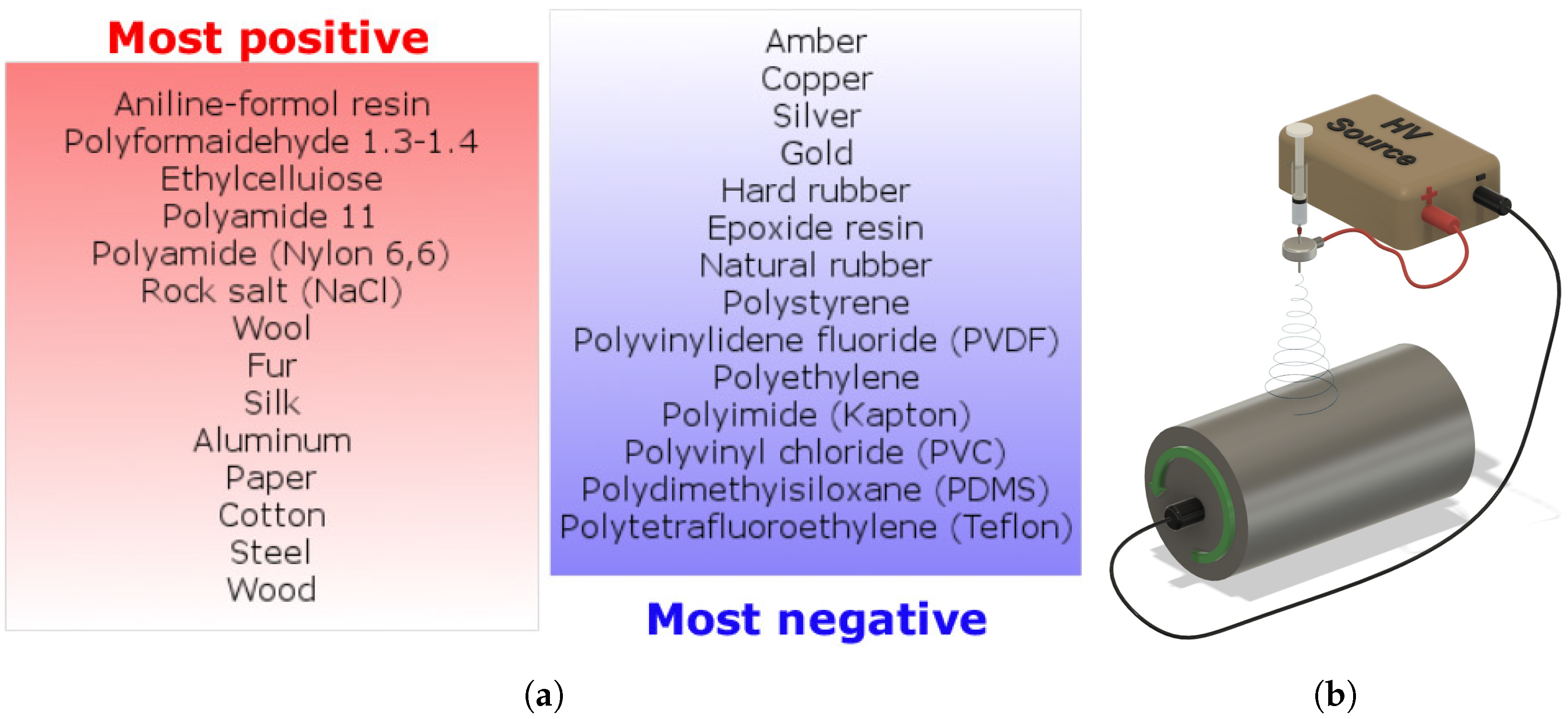
:1. Introduction
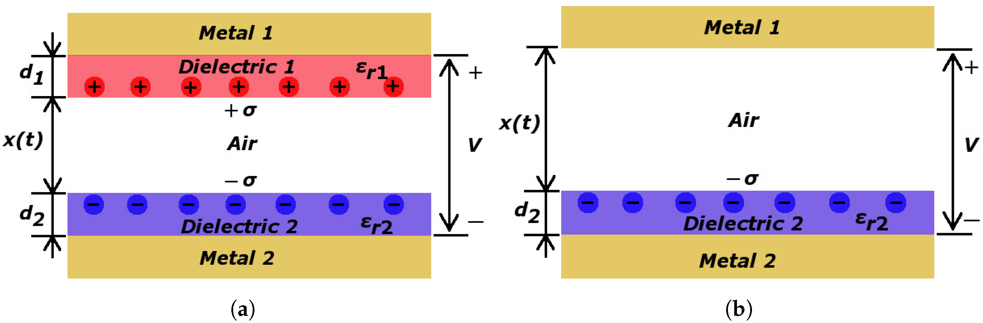
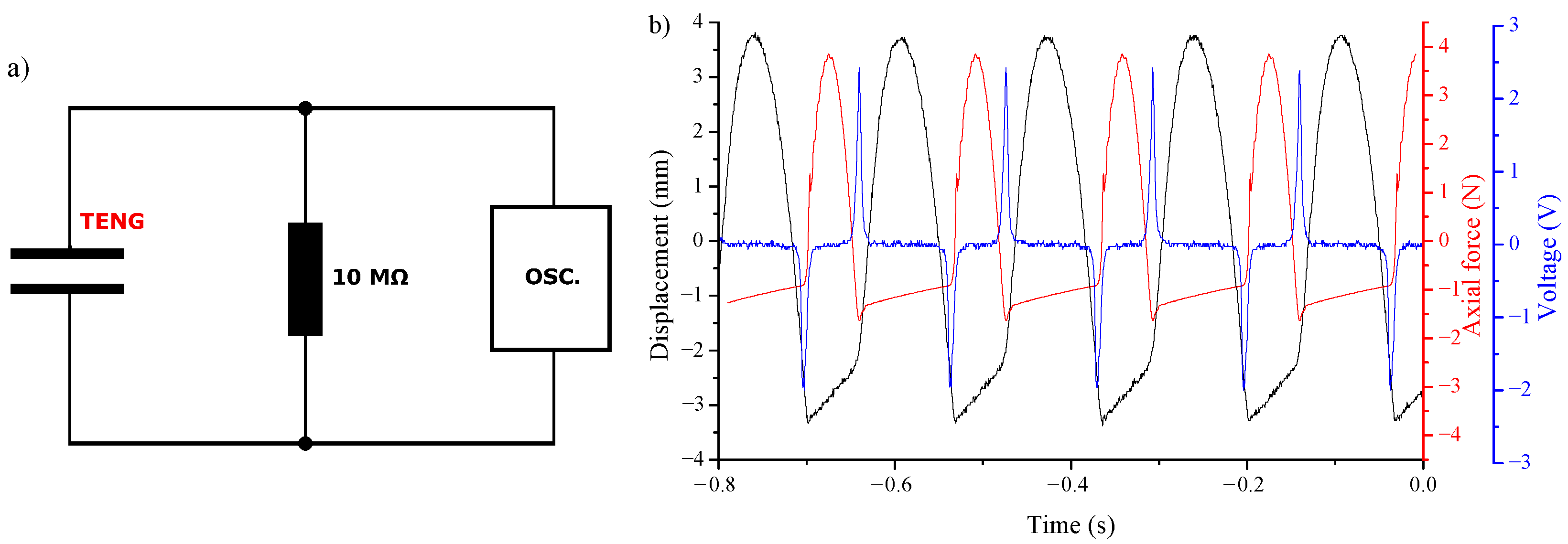
The V-Q-x Relationship for Contact-Separation Mode
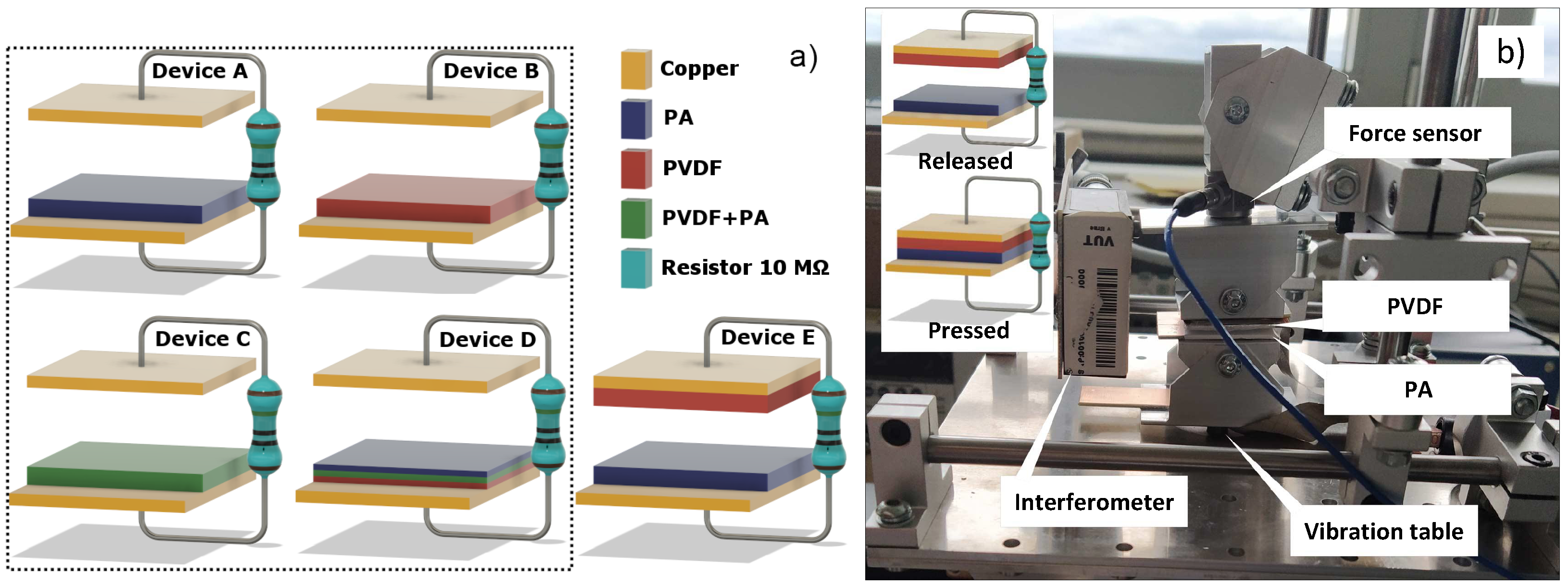
2. Material and Methods
3. Results and Discussion
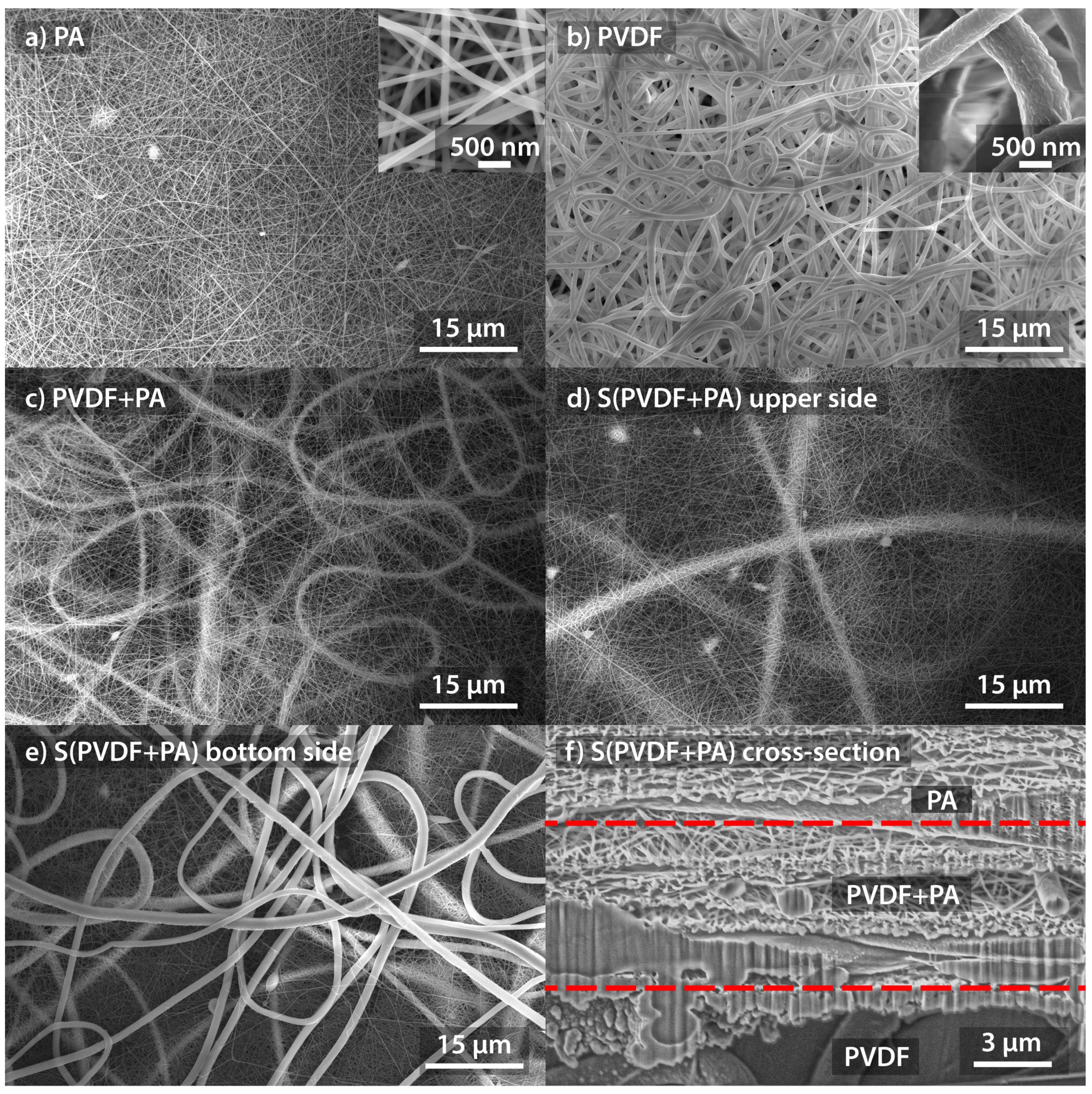
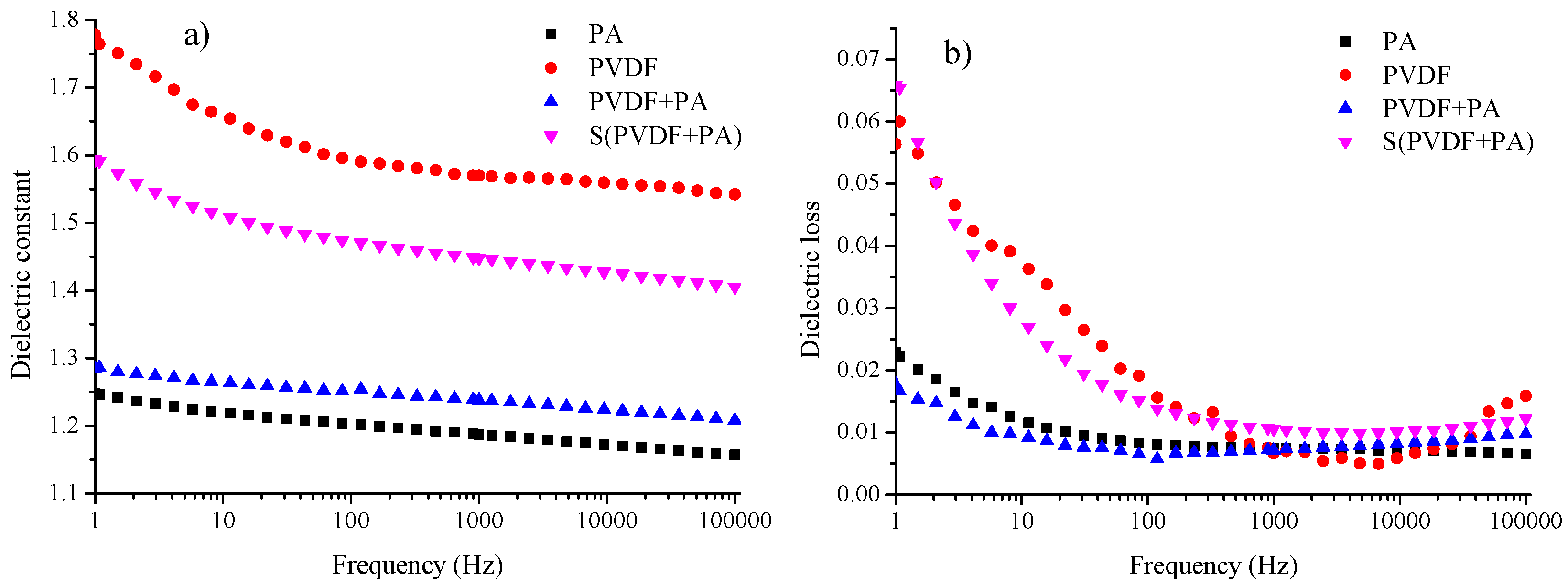
3.1. Dielectric Properties of Electrospun Samples
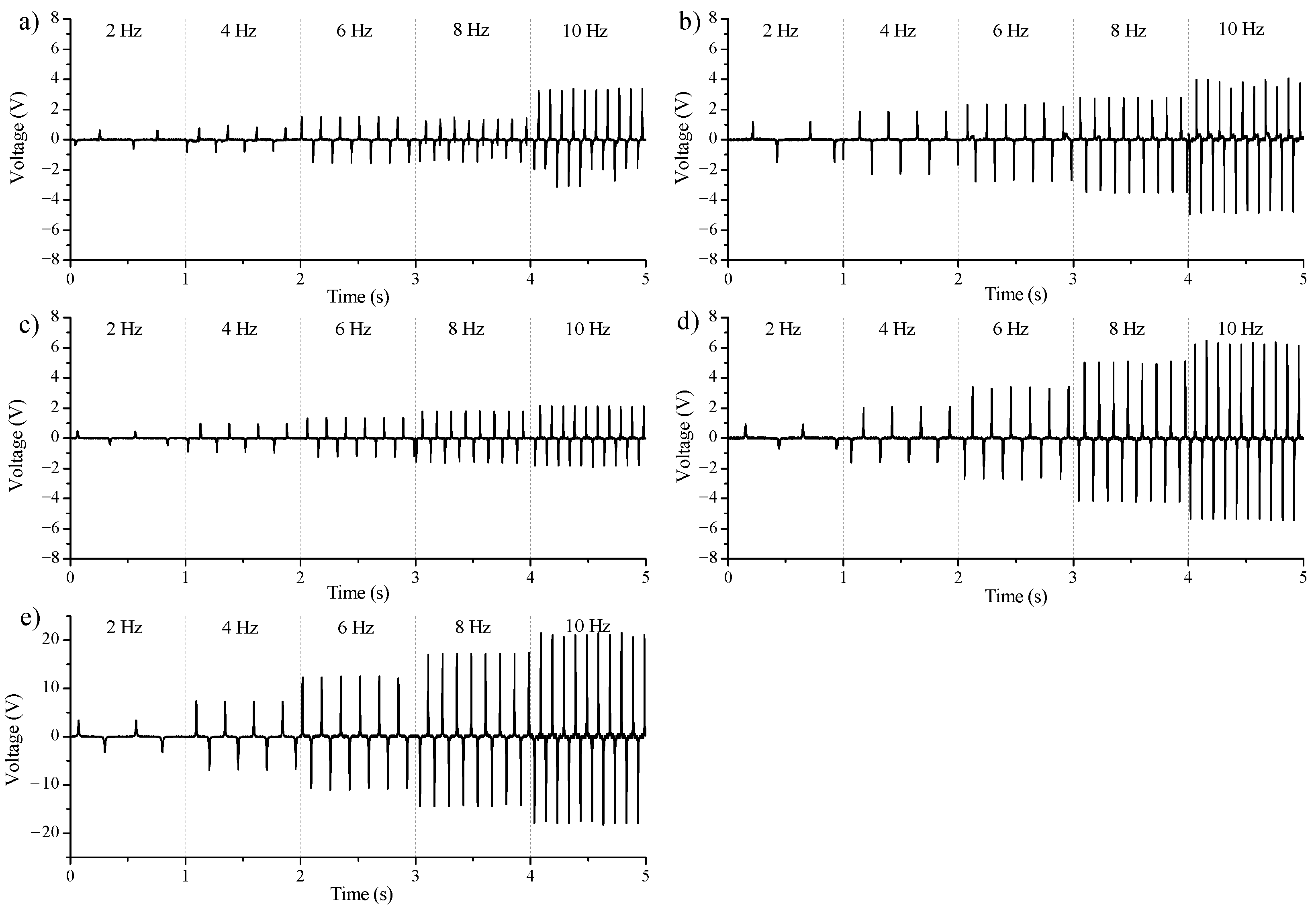
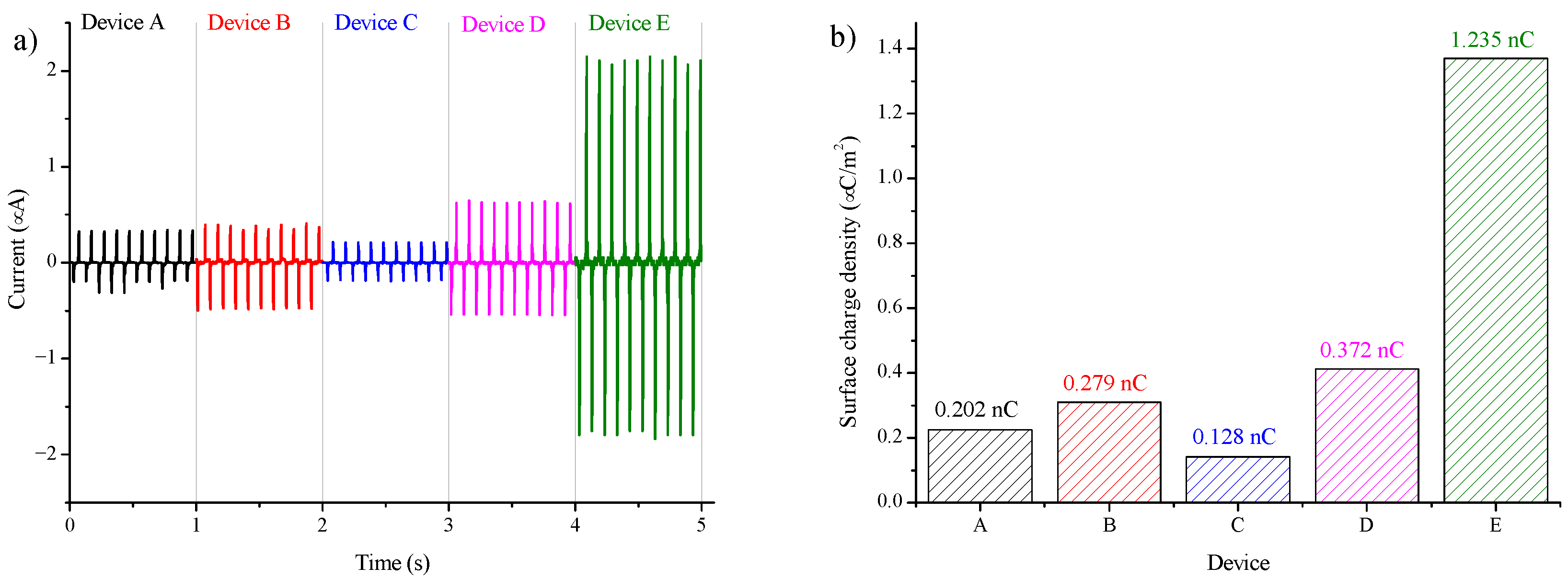
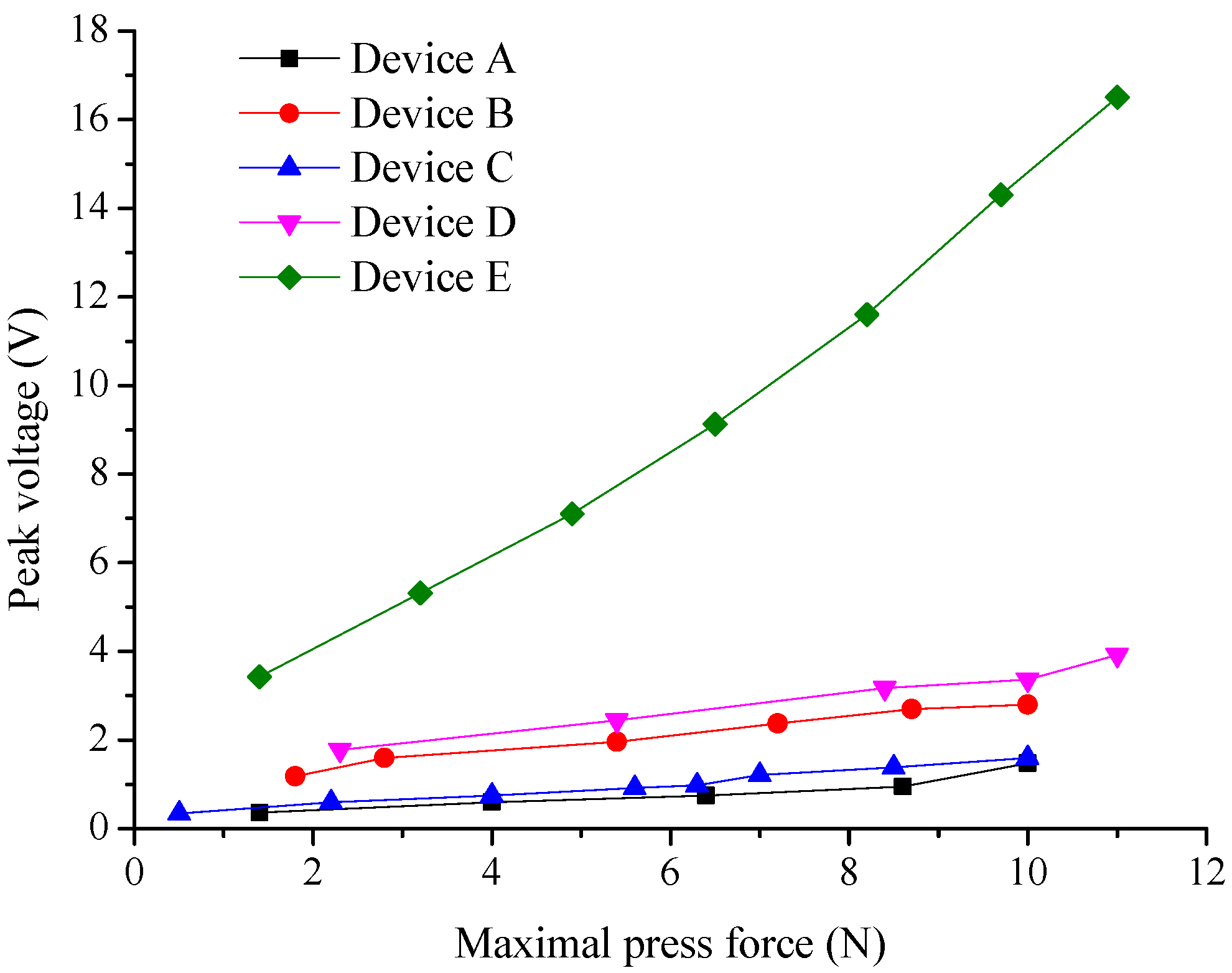
3.2. Triboelectric Properties of Electrospun Samples
4. Conclusions
Author Contributions
Funding
Institutional Review Board Statement
Informed Consent Statement
Conflicts of Interest
Sample Availability
Abbreviations
| AA | Acetic acid |
| Ac | Acetone |
| CS | Contact-separation |
| DMSO | Dimethylsulphoxide |
| FA | Formic acid |
| FT | Freestanding triboelectric-layer |
| LS | Lateral sliding |
| PA | Polyamide 6 |
| PDMS | Polydimethylsiloxane |
| PVDF | Polyvinylidene fluoride |
| SE | Single-electrode |
| SEM | Scanning electron microscopy |
| SCD | Surface charge density |
References
- Xiong, J.; Lee, P.S. Progress on wearable triboelectric nanogenerators in shapes of fiber, yarn, and textile. Sci. Technol. Adv. Mater. 2019, 20, 837–857. [Google Scholar] [CrossRef] [Green Version]
- Xia, K.; Wu, D.; Fu, J.; Hoque, N.A.; Ye, Y.; Xu, Z. A high-output triboelectric nanogenerator based on nickel–copper bimetallic hydroxide nanowrinkles for self-powered wearable electronics. J. Mater. Chem. A 2020, 8, 25995–26003. [Google Scholar] [CrossRef]
- Zhang, P.; Zhang, Z.; Cai, J. A foot pressure sensor based on triboelectric nanogenerator for human motion monitoring. Microsyst. Technol. 2021, 27, 3507–3512. [Google Scholar] [CrossRef]
- Heo, D.; Chung, J.; Kim, B.; Yong, H.; Shin, G.; Cho, J.W.; Kim, D.; Lee, S. Triboelectric speed bump as a self-powered automobile warning and velocity sensor. Nano Energy 2020, 72, 104719. [Google Scholar] [CrossRef]
- Chen, T.; Shi, Q.; Li, K.; Yang, Z.; Liu, H.; Sun, L.; Dziuban, J.A.; Lee, C. Investigation of position sensing and energy harvesting of a flexible triboelectric touch pad. Nanomaterials 2018, 8, 613. [Google Scholar] [CrossRef] [PubMed] [Green Version]
- Ibrahim, A.; Ramini, A.; Towfighian, S. Triboelectric energy harvester with large bandwidth under harmonic and random excitations. Energy Rep. 2020, 6, 2490–2502. [Google Scholar] [CrossRef]
- Ghosh, R.; Pin, K.Y.; Reddy, V.S.; Jayathilaka, W.A.; Ji, D.; Serrano-García, W.; Bhargava, S.K.; Ramakrishna, S.; Chinnappan, A. Micro/nanofiber-based noninvasive devices for health monitoring diagnosis and rehabilitation. Appl. Phys. Rev. 2020, 7, 041309. [Google Scholar] [CrossRef]
- Elahi, H.; Munir, K.; Eugeni, M.; Atek, S.; Gaudenzi, P. Energy harvesting towards self-powered iot devices. Energies 2020, 13, 5528. [Google Scholar] [CrossRef]
- Chen, H.; Xing, C.; Li, Y.; Wang, J.; Xu, Y. Triboelectric nanogenerators for a macro-scale blue energy harvesting and self-powered marine environmental monitoring system. Sustain. Energy Fuels 2020, 4, 1063–1077. [Google Scholar] [CrossRef]
- Gu, G.Q.; Han, C.B.; Lu, C.X.; He, C.; Jiang, T.; Gao, Z.L.; Li, C.J.; Wang, Z.L. Triboelectric Nanogenerator Enhanced Nanofiber Air Filters for Efficient Particulate Matter Removal. ACS Nano 2017, 11, 6211–6217. [Google Scholar] [CrossRef]
- Ghatak, B.; Banerjee, S.; Ali, S.B.; Bandyopadhyay, R.; Das, N.; Mandal, D.; Tudu, B. Design of a self-powered triboelectric face mask. Nano Energy 2021, 79, 105387. [Google Scholar] [CrossRef] [PubMed]
- Shi, L.; Jin, H.; Dong, S.; Huang, S.; Kuang, H.; Xu, H.; Chen, J.; Xuan, W.; Zhang, S.; Li, S.; et al. High-performance triboelectric nanogenerator based on electrospun PVDF-graphene nanosheet composite nanofibers for energy harvesting. Nano Energy 2021, 80, 105599. [Google Scholar] [CrossRef]
- Rodrigues, C.; Nunes, D.; Clemente, D.; Mathias, N.; Correia, J.M.; Rosa-Santos, P.; Taveira-Pinto, F.; Morais, T.; Pereira, A.; Ventura, J. Emerging triboelectric nanogenerators for ocean wave energy harvesting: State of the art and future perspectives. Energy Environ. Sci. 2020, 13, 2657–2683. [Google Scholar] [CrossRef]
- Zou, H.; Zhang, Y.; Guo, L.; Wang, P.; He, X.; Dai, G.; Zheng, H.; Chen, C.; Wang, A.C.; Xu, C.; et al. Quantifying the triboelectric series. Nat. Commun. 2019, 10, 1427. [Google Scholar] [CrossRef] [Green Version]
- Wang, Z.L. Triboelectric nanogenerators as new energy technology for self-powered systems and as active mechanical and chemical sensors. ACS Nano 2013, 7, 9533–9557. [Google Scholar] [CrossRef]
- Kim, Y.J.; Lee, J.; Park, S.; Park, C.; Park, C.; Choi, H.J. Effect of the relative permittivity of oxides on the performance of triboelectric nanogenerators. RSC Adv. 2017, 7, 49368–49373. [Google Scholar] [CrossRef] [Green Version]
- Dhakar, L. Triboelectric Devices for Power Generation and Self-Powered Sensing Applications; Springer: Singapore, 2017. [Google Scholar] [CrossRef]
- Částková, K.; Kaštyl, J.; Sobola, D.; Petruš, J.; Šťastná, E.; Říha, D.; Tofel, P. Structure–Properties Relationship of Electrospun PVDF Fibers. Nanomaterials 2020, 10, 1221. [Google Scholar] [CrossRef]
- Sobola, D.; Kaspar, P.; Částková, K.; Dallaev, R.; Papež, N.; Sedlák, P.; Trčka, T.; Orudzhev, F.; Kaštyl, J.; Weiser, A.; et al. PVDF Fibers Modification by Nitrate Salts Doping. Polymers 2021, 13, 2439. [Google Scholar] [CrossRef]
- Černohorský, P.; Pisarenko, T.; Papež, N.; Sobola, D.; Ţălu, Ş.; Částková, K.; Kaštyl, J.; Macků, R.; Škarvada, P.; Sedlák, P. Structure Tuning and Electrical Properties of Mixed PVDF and Nylon Nanofibers. Materials 2021, 14, 6096. [Google Scholar] [CrossRef]
- Kaspar, P.; Sobola, D.; Částková, K.; Knápek, A.; Burda, D.; Orudzhev, F.; Dallaev, R.; Tofel, P.; Trčka, T.; Grmela, L.; et al. Characterization of Polyvinylidene Fluoride (PVDF) Electrospun Fibers Doped by Carbon Flakes. Polymers 2020, 12, 2766. [Google Scholar] [CrossRef]
- Wang, W.; Wang, H.; Wang, H.; Jin, X.; Li, J.; Zhu, Z. Electrospinning preparation of a large surface area, hierarchically porous, and interconnected carbon nanofibrous network using polysulfone as a sacrificial polymer for high performance supercapacitors. RSC Adv. 2018, 8, 28480–28486. [Google Scholar] [CrossRef] [Green Version]
- Chen, F.; Wu, Y.; Ding, Z.; Xia, X.; Li, S.; Zheng, H.; Diao, C.; Yue, G.; Zi, Y. A novel triboelectric nanogenerator based on electrospun polyvinylidene fluoride nanofibers for effective acoustic energy harvesting and self-powered multifunctional sensing. Nano Energy 2019, 56, 241–251. [Google Scholar] [CrossRef]
- Garain, S.; Jana, S.; Sinha, T.K.; Mandal, D. Design of in Situ Poled Ce3+-Doped Electrospun PVDF/Graphene Composite Nanofibers for Fabrication of Nanopressure Sensor and Ultrasensitive Acoustic Nanogenerator. ACS Appl. Mater. Interfaces 2016, 8, 4532–4540. [Google Scholar] [CrossRef] [PubMed]
- Mi, H.Y.; Jing, X.; Zheng, Q.; Fang, L.; Huang, H.X.; Turng, L.S.; Gong, S. High-performance flexible triboelectric nanogenerator based on porous aerogels and electrospun nanofibers for energy harvesting and sensitive self-powered sensing. Nano Energy 2018, 48, 327–336. [Google Scholar] [CrossRef]
- Gasparini, C.; Aluigi, A.; Pace, G.; Molina-García, M.A.; Treossi, E.; Ruani, G.; Candini, A.; Melucci, M.; Bettin, C.; Bonaccorso, F.; et al. Enhancing triboelectric performances of electrospun poly(vinylidene fluoride) with graphene oxide sheets. Graphene Technol. 2020, 5, 49–57. [Google Scholar] [CrossRef]
- Ţălu, Ş. Micro and Nanoscale Characterization of Three Dimensional Surfaces: Basics and Applications; Napoca Star Publishing House: Cluj-Napoca, Romania, 2015. [Google Scholar]
- Zhang, F.; Li, B.; Zheng, J.; Xu, C. Facile Fabrication of Micro-Nano Structured Triboelectric Nanogenerator with High Electric Output. Nanoscale Res. Lett. 2015, 10, 4–9. [Google Scholar] [CrossRef] [Green Version]
- Yu, J.; Hou, X.; He, J.; Cui, M.; Wang, C.; Geng, W.; Mu, J.; Han, B.; Chou, X. Ultra-flexible and high-sensitive triboelectric nanogenerator as electronic skin for self-powered human physiological signal monitoring. Nano Energy 2020, 69, 104437. [Google Scholar] [CrossRef]
- Feng, Y.; Zheng, Y.; Zhang, G.; Wang, D.; Zhou, F.; Liu, W. A new protocol toward high output TENG with polyimide as charge storage layer. Nano Energy 2017, 38, 467–476. [Google Scholar] [CrossRef]
- Kim, D.W.; Lee, J.H.; You, I.; Kim, J.K.; Jeong, U. Adding a stretchable deep-trap interlayer for high-performance stretchable triboelectric nanogenerators. Nano Energy 2018, 50, 192–200. [Google Scholar] [CrossRef]
- Chen, A.; Zhang, C.; Zhu, G.; Wang, Z.L. Polymer Materials for High-Performance Triboelectric Nanogenerators. Adv. Sci. 2020, 7, 1–25. [Google Scholar] [CrossRef] [PubMed]
- Garcia, C.; Trendafilova, I.; de Villoria, R.G.; del Rio, J.S. Self-powered pressure sensor based on the triboelectric effect and its analysis using dynamic mechanical analysis. Nano Energy 2018, 50, 401–409. [Google Scholar] [CrossRef] [Green Version]
- Wu, C.; Wang, A.C.; Ding, W.; Guo, H.; Wang, Z.L. Triboelectric Nanogenerator: A Foundation of the Energy for the New Era. Adv. Energy Mater. 2019, 9, 1802906. [Google Scholar] [CrossRef]
- Taghavi, M.; Beccai, L. A contact-key triboelectric nanogenerator: Theoretical and experimental study on motion speed influence. Nano Energy 2015, 18, 283–292. [Google Scholar] [CrossRef]
- Niu, S.; Wang, S.; Lin, L.; Liu, Y.; Zhou, Y.S.; Hu, Y.; Wang, Z.L. Theoretical study of contact-mode triboelectric nanogenerators as an effective power source. Energy Environ. Sci. 2013, 6, 3576. [Google Scholar] [CrossRef]
- Zhang, H.; Yao, L.; Quan, L.; Zheng, X. Theories for triboelectric nanogenerators: A comprehensive review. Nanotechnol. Rev. 2020, 9, 610–625. [Google Scholar] [CrossRef]
- Smejkalová, T.; Ţălu, Ş.; Dallaev, R.; Částková, K.; Sobola, D.; Nazarov, A. SEM imaging and XPS characterization of doped PVDF fibers. E3S Web Conf. 2021, 270, 01011. [Google Scholar] [CrossRef]
- Misiurev, D.; Ţălu, Ş.; Dallaev, R.; Sobola, D.; Goncharova, M. Preparation of PVDF-CNT composite. In E3S Web of Conferences; EDP Sciences: Les Ulis, France, 2021; Volume 270, p. 01012. [Google Scholar] [CrossRef]
- Roscow, J.I.; Lewis, R.W.; Taylor, J.; Bowen, C.R. Modelling and fabrication of porous sandwich layer barium titanate with improved piezoelectric energy harvesting figures of merit. Acta Mater. 2017, 128, 207–217. [Google Scholar] [CrossRef]
- Tong, J.; Zhang, H.; Li, W.; Chen, H.; Wang, D.; Hu, M.; Wang, Z. Simultaneously improving thermal conductivity and dielectric properties of poly(vinylidene fluoride)/expanded graphite via melt blending with polyamide 6. J. Appl. Polym. Sci. 2021, 138, 51354. [Google Scholar] [CrossRef]
- Song, Y.; Shen, Y.; Hu, P.; Lin, Y.; Li, M.; Nan, C.W. Significant enhancement in energy density of polymer composites induced by dopamine-modified Ba 0.6Sr 0.4TiO 3 nanofibers. Appl. Phys. Lett. 2012, 101, 152904. [Google Scholar] [CrossRef]


| Sample | Structure | Needle (–) | Rotation Speed (rpm) |
|---|---|---|---|
| PA | PA fibers | 19G | 300 |
| PVDF | PVDF fibers | 17G | 300 |
| PVDF+PA | PVDF+PA intertwined fibers | 17G/19G | 300 |
| S(PVDF+PA) | PVDF//PVDF+PA//PA * | see above | 2000 |
| Device | Type of the Triboelectric Device | Fiber Dielectric Sample | εr at 1 kHz | tan δ (×103) at 1 kHz | Peak Voltage (V) at F = 10 N, f = 6 Hz | Triboelectric Response |
|---|---|---|---|---|---|---|
| A | Conductor-to-dielectric | PA | 1.19 | 7.44 | 1.5 | Lowest |
| B | PVDF | 1.57 | 6.68 | 2.8 | Medium | |
| C | PVDF+PA | 1.24 | 7.17 | 1.6 | Low | |
| D | S(PVDF+PA) | 1.45 | 10.56 | 3.5 | High | |
| E | Dielectric-to-dielectric | PVDF opposite PA | 1.57 PVDF | 6.68 PVDF | 14.2 | Highest |
| 1.19 PA | 7.44 PA |
Publisher’s Note: MDPI stays neutral with regard to jurisdictional claims in published maps and institutional affiliations. |
© 2022 by the authors. Licensee MDPI, Basel, Switzerland. This article is an open access article distributed under the terms and conditions of the Creative Commons Attribution (CC BY) license (https://creativecommons.org/licenses/by/4.0/).
Share and Cite
Tofel, P.; Částková, K.; Říha, D.; Sobola, D.; Papež, N.; Kaštyl, J.; Ţălu, Ş.; Hadaš, Z. Triboelectric Response of Electrospun Stratified PVDF and PA Structures. Nanomaterials 2022, 12, 349. https://doi.org/10.3390/nano12030349
Tofel P, Částková K, Říha D, Sobola D, Papež N, Kaštyl J, Ţălu Ş, Hadaš Z. Triboelectric Response of Electrospun Stratified PVDF and PA Structures. Nanomaterials. 2022; 12(3):349. https://doi.org/10.3390/nano12030349
Chicago/Turabian StyleTofel, Pavel, Klára Částková, David Říha, Dinara Sobola, Nikola Papež, Jaroslav Kaštyl, Ştefan Ţălu, and Zdeněk Hadaš. 2022. "Triboelectric Response of Electrospun Stratified PVDF and PA Structures" Nanomaterials 12, no. 3: 349. https://doi.org/10.3390/nano12030349
APA StyleTofel, P., Částková, K., Říha, D., Sobola, D., Papež, N., Kaštyl, J., Ţălu, Ş., & Hadaš, Z. (2022). Triboelectric Response of Electrospun Stratified PVDF and PA Structures. Nanomaterials, 12(3), 349. https://doi.org/10.3390/nano12030349