Article

Steep-Slope and Hysteresis-Free MoS2 Negative-Capacitance Transistors Using Single HfZrAlO Layer as Gate Dielectric

School of Optical and Electronic Information, Huazhong University of Science and Technology, Wuhan 430074, China
*
Author to whom correspondence should be addressed.
These authors contributed equally to this work.
Nanomaterials 2022, 12(24), 4352; https://doi.org/10.3390/nano12244352
Submission received: 22 October 2022 / Revised: 12 November 2022 / Accepted: 14 November 2022 / Published: 7 December 2022

Abstract

:
An effective way to reduce the power consumption of an integrated circuit is to introduce negative capacitance (NC) into the gate stack. Usually, negative-capacitance field-effect transistors (NCFETs) use both a negative-capacitance layer and a positive-capacitance layer as the stack gate, which is not conductive to the scaling down of devices. In this study, a steep-slope and hysteresis-free MoS2 NCFET is fabricated using a single Hf0.5−xZr0.5−xAl2xOy (HZAO) layer as the gate dielectric. By incorporating several Al atoms into the Hf0.5Zr0.5O2 (HZO) thin film, negative capacitance and positive capacitance can be achieved simultaneously in the HZAO thin film and good capacitance matching can be achieved. This results in excellent electrical performance of the relevant NCFETs, including a low sub-threshold swing of 22.3 mV/dec over almost four orders of drain-current magnitude, almost hysteresis-free, and a high on/off current ratio of 9.4 × 10⁶. Therefore, using a single HZAO layer as the gate dielectric has significant potential in the fabrication of high-performance and low-power dissipation NCFETs compared to conventional HZO/Al2O3 stack gates.

1. Introduction

As the size of MOSFETs continues to decrease, it has become increasingly difficult to reduce the size of the device below 10 nm. One reason for this is that the power consumption of the device is difficult to reduce. In traditional MOSFETs, the sub-threshold swing (SS) of the device is limited by the Boltzmann limit, resulting in the chip power consumption failing to reach the expected target [1,2,3,4,5]. To reduce the device power consumption, several novel device models have been proposed to achieve a sub-threshold swing (SS) lower than 60 mV/dec at room temperature. The first type proposed is the nano-electromechanical switch (NEM) [6,7]. The NEM is small and low in power consumption. Its SS can even reach single digits, to much lower than 60 mV/dec. However, the reliability of NEM devices is relatively low and the lack of expandable preparation technology is not conducive to large-scale process production. Another low-power device model is the tunnel field-effect transistor (TFET) [8,9,10,11]. In 2017, Adrian Jonescu proposed using the quantum tunneling effect to make TFETs. TFETs can significantly reduce the driving voltage imposed by the gate and have a very low turn-off current. Their SS can be lower than 60 mV/dec, with greatly reduced power consumption. However, the turn-on current is relatively low and the choice of materials, and the presence of defects in these, significantly impact the development of TFETs. The negative-capacitance field-effect transistor (NCFET) is considered an ideal choice for ultra-low power applications [1,2,4,12,13,14]. It only requires addition of a ferroelectric material as an additional layer to the gate dielectric layer of a traditional MOSFET to act as a negative capacitor to achieve voltage amplification of the channel surface potential, thus breaking the Boltzmann limit such that an SS less than 60 mV/dec can be achieved. At the same time, materials with high dielectric constants, such as HfO2 and ZrO2, having much higher dielectric constants than SiO2, wide band gaps and good thermal stability, are considered excellent gate dielectric materials and have been applied in process mass production. However, in Germany, Johannes Muller et al. reported that ferroelectric properties would appear when different elements, such as Si, Y, Al and Zr, were doped into HfO2 thin films, [15,16,17]. This discovery resulted in ferroelectric materials and NCFET becoming an international research craze [18,19,20,21]. Using HZO thin film as the ferroelectric layer, HZO NCFETs have become one of the solutions to achieving ultra-low-power CMOS technology. HZO NCFETs have the following advantages: (1) high conduction current; (2) symmetrical circuit layout; and (3) CMOS process compatibility. However, these NCFETs contain at least two layers as the gate stack, which complicates the fabrication process and is not conducive to the scaling down of devices.
In this investigation, a single-layer (HfZr)0.5−0.5xAlxOy (HZAO) thin film was found to have both negative capacitance and positive capacitance due to its ferroelectricity, and, thus, capacitance matching could be realized by itself. A single HZAO layer was used as the gate dielectric to fabricate the relevant MoS2 NCFETs. By optimizing the Al content and the annealing temperature of the HZAO thin film, excellent electrical properties for NCFETs have been achieved, including a low SS of 22.3 mV/dec over almost four orders of drain-current magnitude, almost no hysteresis, and a high on/off current ratio of 9.4 × 10⁷, which, so far, is better than that achieved with HZO-based MoS2 NCFETs under the same fabrication and measurement conditions.

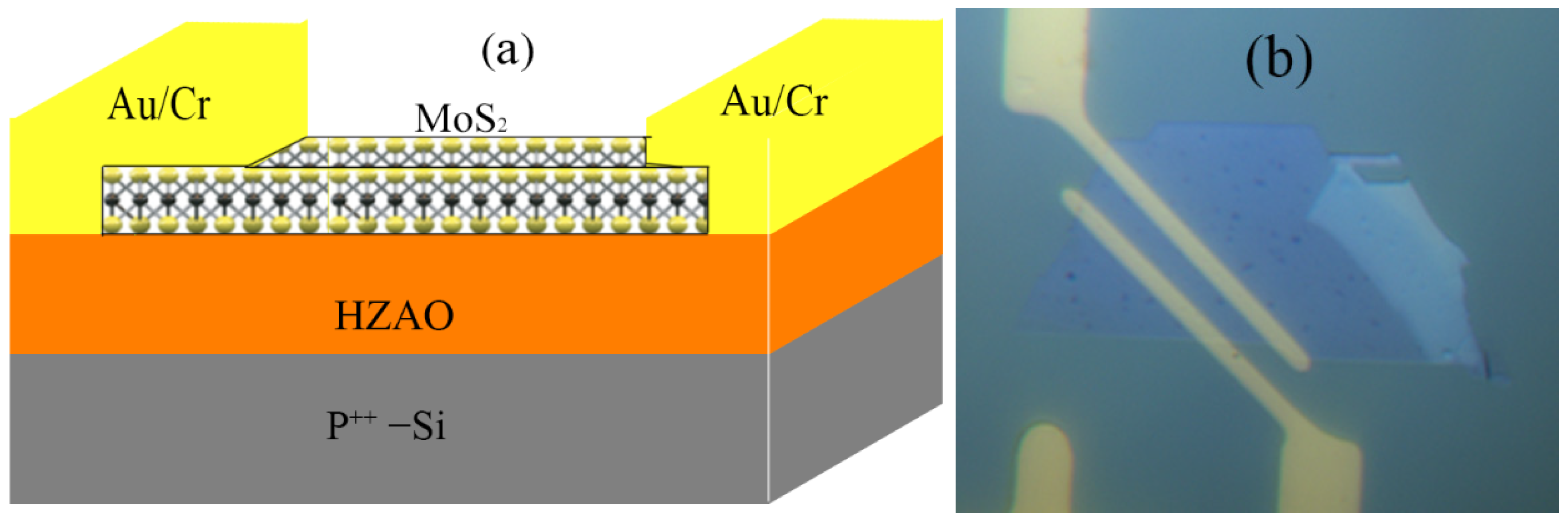
2. Experimental Method

Heavily-doped p++-Si wafers with a resistivity of 0.005~0.01 Ω·cm were cleaned by a standard RCA method as substrate/back gate and then were placed in an atom-layer deposition (ALD) chamber. As the ferroelectricity of the HZAO thin film is highly dependent on its annealing temperature and atom ratio [19,22,23], HZAO thin films with different atom ratios were prepared through alternately ALD-depositing Al2O3, HfO2 and ZrO2 at ratios of Al2O3:HfO2:ZrO2 = 1:5:5 or 1:10:10 or 1:20:20 or 0:1:1 to yield a nano-laminate Hf0.4Zr0.4Al0.2Oy or Hf0.45Zr0.45Al0.1Oy or Hf0.475Zr0.475Al0.05Oy or Hf0.5Zr0.5Oy (HZO) thin film on the p++-Si substrate using trimethylaluminium (TMA) as the Al source, tetrakis (ethylmethylamino)-Hf (TDMAH) as the Hf source, tetrakis (ethylmethylamino)-Zr (TDMAZ) as the Zr source, and H2O as the oxidant. During deposition, the temperatures of the substrate and the Hf/Zr sources were 200 °C and 75 °C, respectively. The resultant thicknesses of the thin films were 8.03 nm, 8.01 nm, 8.03 nm, and 8.00 nm, respectively, measured by ellipsometry. The thin films were then annealed by rapid thermal processing (RTP) at 600 °C, 650 °C, 700 °C and 750 °C, respectively, for a duration of 30 s.
MoS2 flakes were transferred from bulk crystal onto the HZAO or HZO/p++-Si substrates by a micromechanical exfoliating method using 3M tapes and PDMS films [24]. Electron-beam lithography (EBL) was used to pattern the source (S) and drain (D) electrodes of the transistors, followed by deposition of 15 nm Cr and 45-nm Au at room temperature by thermal evaporation and a lift-off process to form the S/D electrodes [25,26,27]. The drawn channel length (L) of these transistors was 3 μm and the channel width (W) was 3~5 μm, based on the shape of the flakes. Lastly, the transistors were annealed at 300 °C for 180 s in a N2 environment to improve the electrical contact between the MoS2 and metal electrode and to remove the gas and liquid molecules on the MoS2 [28].
A schematic diagram of a back-gated NCFET is shown in Figure 1a and its optical micrograph is shown in Figure 1b.

3. Results and Discussion

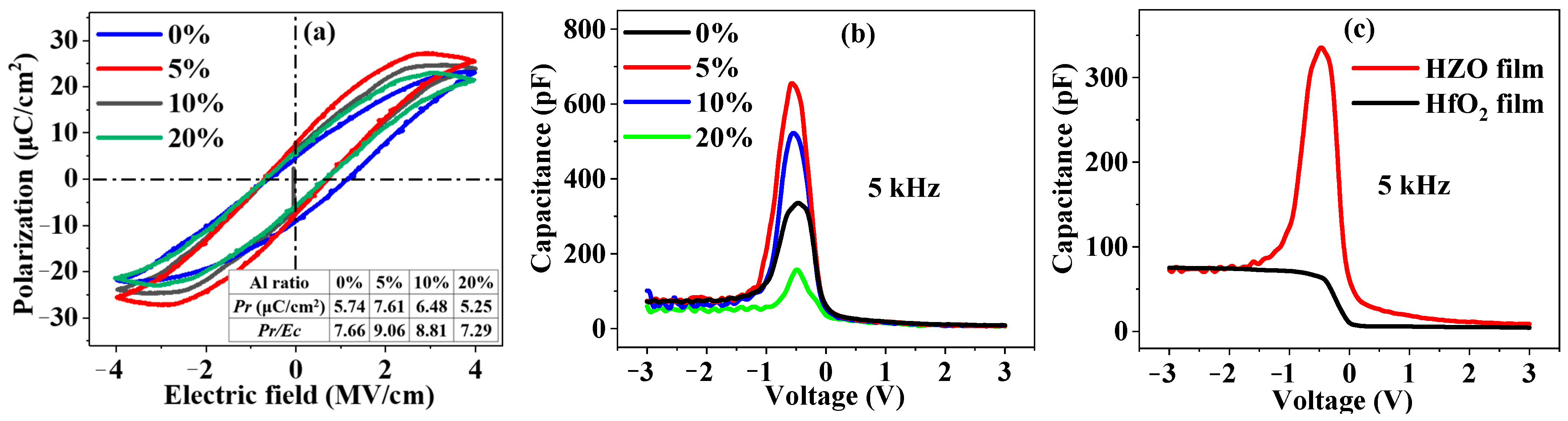
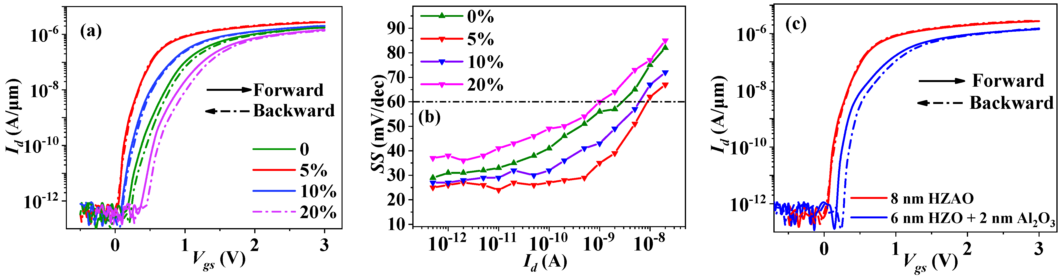
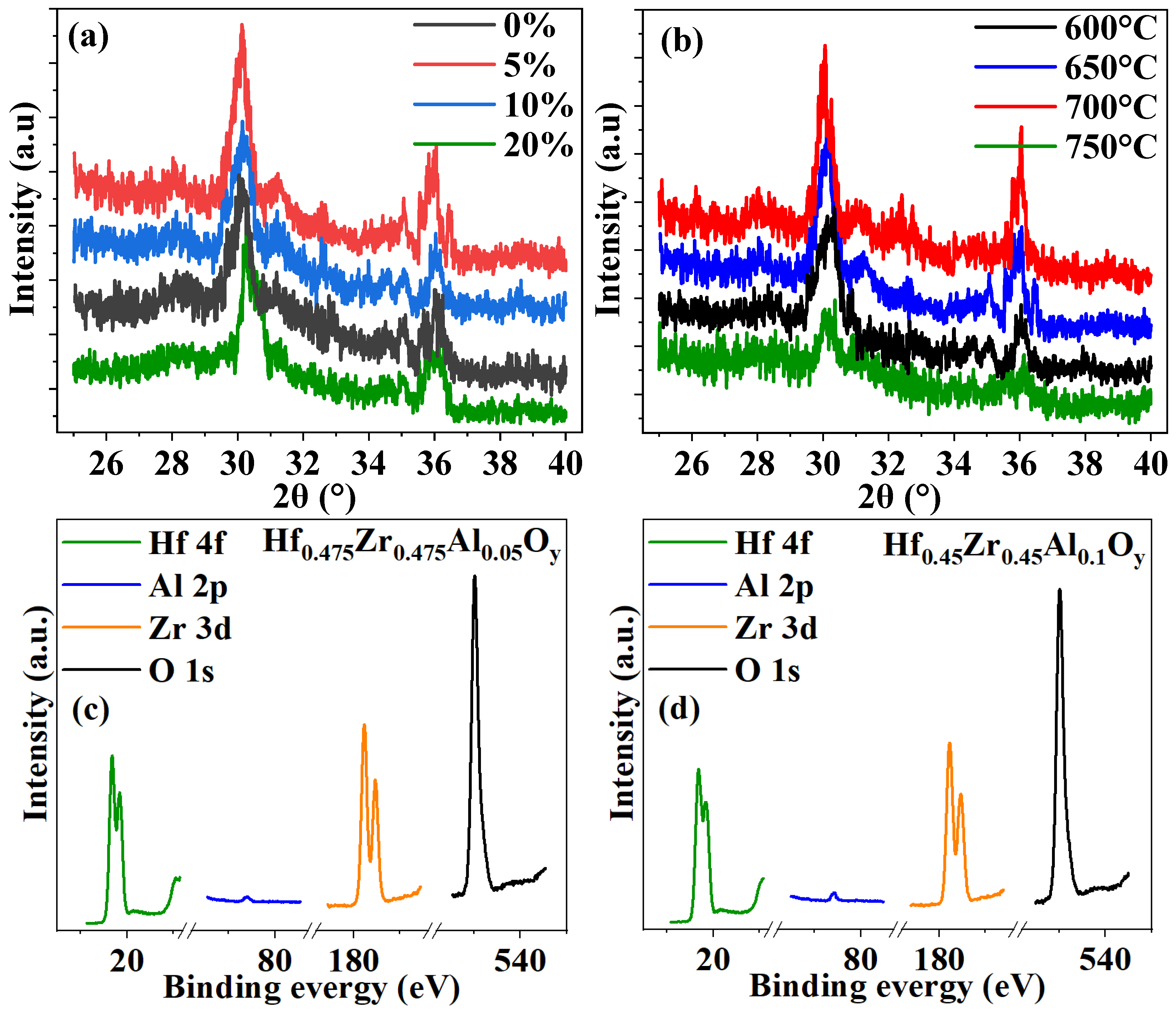
3.1. Optimization of Al Content in HZAO Thin Film

The polarization vs. field (P-E) measurements were carried out on the (Au/Cr)/HZAO/p++-Si capacitor to characterize the ferroelectricity of the HZAO thin films at a frequency of 50 Hz at room temperature in light-tight condition, with Au/Cr as the top electrode and p++-Si as the bottom electrode. Figure 2a shows the P-E curves of the Hf0.4Zr0.4Al0.2Oy, Hf0.45Zr0.45Al0.1Oy, Hf0.475Zr0.475Al0.05Oy and Hf0.5Zr0.5O samples; the inset shows the extracted ferroelectric parameters. The Hf0.475Zr0.475Al0.05Oy thin film exhibited the strongest ferroelectricity, with a total remnant polarization (2|Pr|) of 15.22 μC/cm2 and a Pr/Ec ratio of 9.06 pF/cm (Ec is the coercive field), indicating that the ferroelectricity of the HZO thin film could be enhanced by incorporation of Al with a suitable content (e.g., 5% Al in an HZO thin film).
The capacitance-voltage (C-V) curves of the (Au/Cr)/HZAO/p++-Si capacitors were measured by an Agilent 4284A precision LCR meter. Figure 2b shows the C-V curves of the HZAO thin films with different Al contents under 5 kHz frequency. A sharp capacitance peak can be observed around 0 V; the higher peak indicates stronger ferroelectricity and a negative-capacitance effect [29]. For the conventional (Cr/Au)/HfO2/p-Si MOS capacitor in Figure 2c, we did not observe a capacitance peak, which would exclude the impact of stresses or high frequency signals. The Hf0.475Zr0.475Al0.05Oy thin film exhibited the highest capacitance peak, which was consistent with the P-E measurement result, indicating that the strongest ferroelectricity was for the Hf0.475Zr0.475Al0.05Oy thin film. The peaks indicate that the single layer HZAO film had both positive- and negative-capacitance characteristics and was able to achieve capacitance-matching by itself without another positive capacitance layer.
The drain current vs. gate-source voltage (Id-Vgs) curves of the transistors were measured using a Keithley 4200 SCS semiconductor parameter analyzer in a light-tight and electrically-shielded probe station in an atmospheric pressure environment at room temperature, as shown in Figure 3a. The sweeping range of Vgs was from −1 V to 3 V, with a sweeping rate of 0.2 V/s and drain-source voltage (Vds) fixed at 50 mV. The SS-Id relations were extracted from the transfer curves and are shown in Figure 3b.
Table 1 lists the off-current (Ioff), on-current (Ion), mobility, SS and hysteresis of the HZAO NCFETs with different Al contents, which were extracted from their relevant transfer curves.
From Figure 3 and Table 1, it can be seen that the HZAO NCFETs with different Al contents exhibited similar Ioff and mobility, indicating that the insulation integrity of the HfZrO thin film was not influenced by the incorporation of Al atoms. It is especially worth noting that the Hf0.475Zr0.475Al0.05Oy NCFET (Al content of 5%) exhibited the lowest SS (22.3 mV/dec) over almost four orders of Id magnitude, the largest Ion (2.8 μA/μm) and the smallest hysteresis (~10 mV) among all the samples, i.e., a suitable Al-doped concentration was determined to be 5%, at which a high switching speed from the off-state to the on-state can be obtained. In addition, comparison of electrical properties between the single-layer HZAO and traditional multi-layer gate stack NCFETs was performed, as shown in Figure 3c and Table 2. For the same thickness of the gate stack, the former exhibited better electrical parameters than the latter. According to the formulas of SS = ( l n 10 ) × ( k B T q ) × ( 1 + C s + C i t C o x ) and C i t = q 2 D i t [30], the interface-state density between MoS2 and positive HZAO was determined to be in a range of (2.75~2.94) × 1012 eV−1cm−2, which would not lead to relatively large hysteresis.

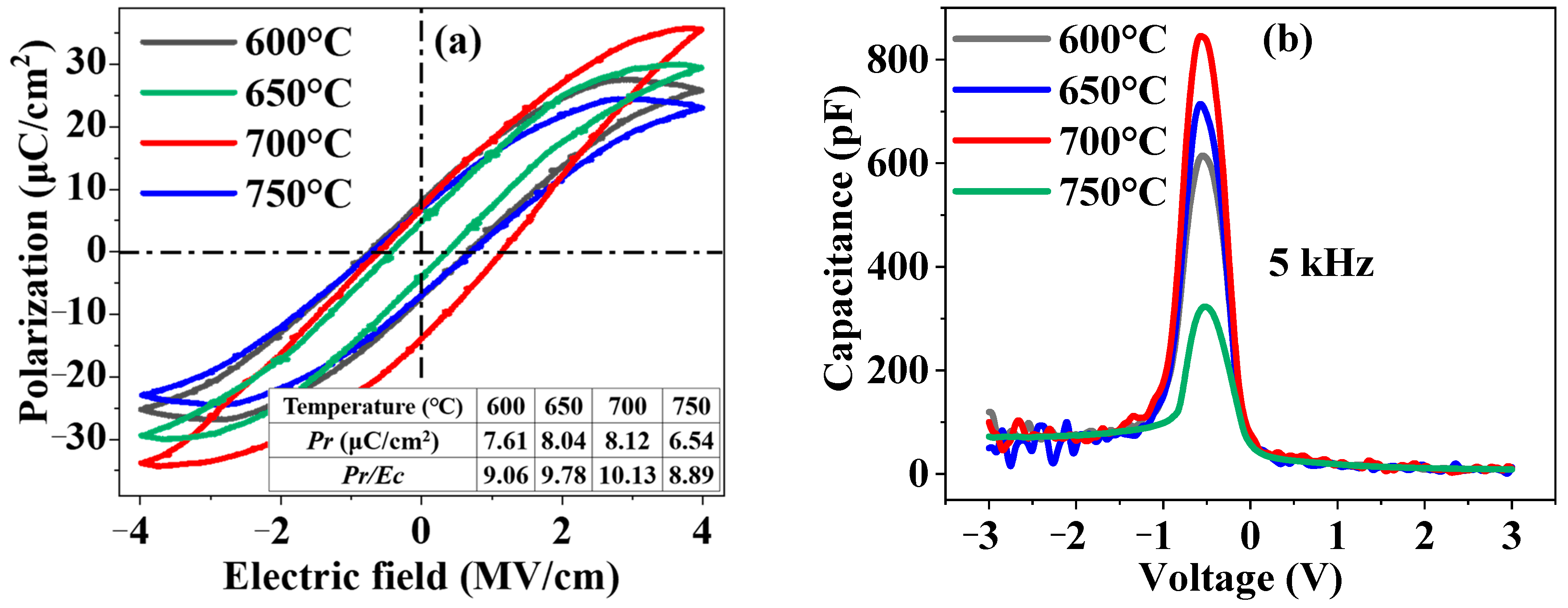
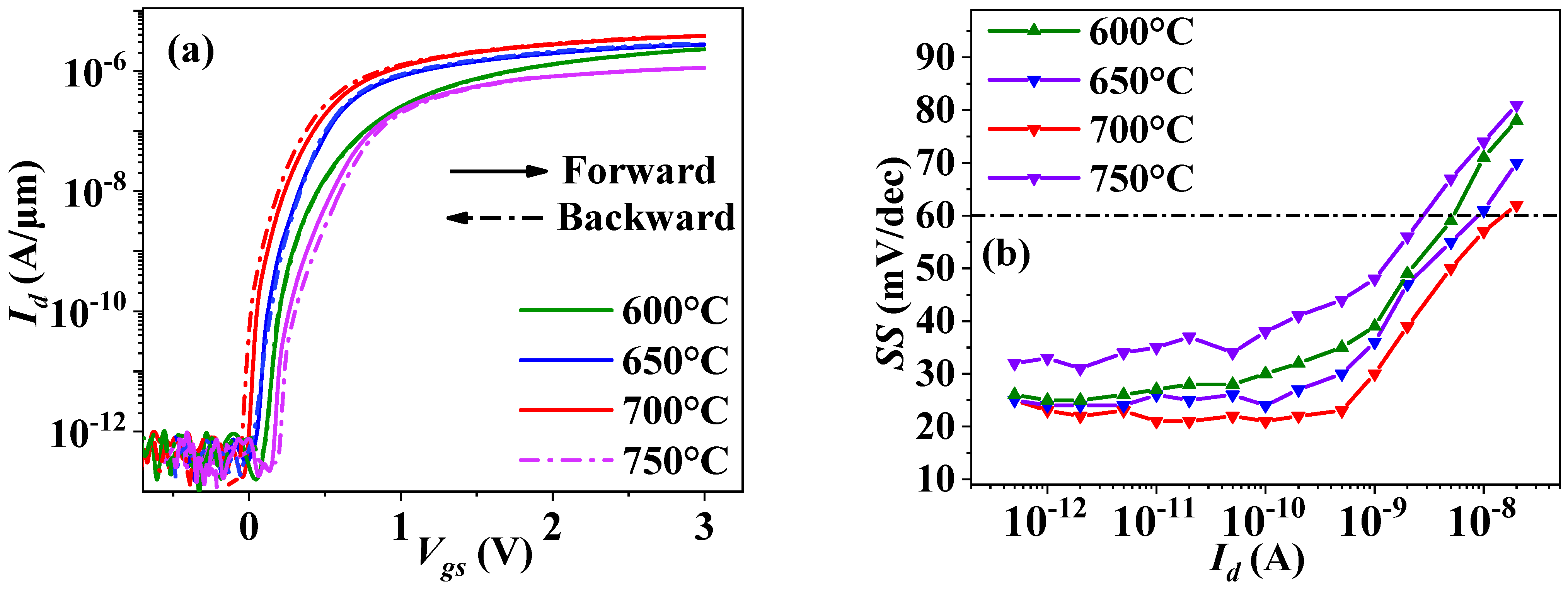
3.2. Optimization of Annealing Temperature

Based on the above results, the Hf0.475Zr0.475Al0.05Oy thin film was selected to investigate its optimum annealing temperature. The P-E curves of the Hf0.475Zr0.475Al0.05Oy thin films annealed at 600 °C, 650 °C, 700 °C and 750 °C, respectively, are shown in Figure 4a. The 700 °C annealed Hf0.475Zr0.475Al0.05Oy thin film exhibited the strongest ferroelectricity, with |2Pr| of 15.76 μC/cm2 and a Pr/Ec ratio of 9.27 pF/cm.
The C-V curves of the (Au/Cr)/Hf0.475Zr0.475Al0.05Oy/p++-Si capacitors for different annealing temperatures were measured at 5 kHz, as shown in Figure 4b. The Hf0.475Zr0.475Al0.05Oy thin film annealed at 700 °C exhibited the highest capacitance peak, which was consistent with the P-E measurement result, supporting it exhibiting the strongest ferroelectricity, as shown in Figure 4a.
The Id-Vgs curves and the SS-Id curves of the Hf0.475Zr0.475Al0.05Oy NCFETs for different annealing temperatures are shown in Figure 5a,b, respectively; the relevant electrical parameters extracted from their transfer curves are listed in Table 2.
From Figure 5 and Table 3, it can be observed that the Hf0.475Zr0.475Al0.05Oy NCFET annealed at 700 °C exhibited the lowest SS (20.4 mV/dec) by almost four orders of Id magnitude with a very small anticlockwise hysteresis of −5~−10 mV, attributed to its enhanced ferroelectricity (large Pr/Ec ratio and |2Pr|), as shown in Figure 4a, resulting in a large ferroelectric capacitance (|CFE|) and, thus, a better capacitance match [31,32]. However, the 650 °C-annealed NCFET exhibited the second lowest SS (22.3 mV/dec) without hysteresis. This is because the hysteresis of the MoS2 NCFETs is influenced by both the interface states and the NC effect. The hysteresis caused by interfacial defaults is clockwise [33] and an anticlockwise hysteresis is introduced by the NC effect of the ferroelectric thin film [1]. So, the total hysteresis for the MoS2 NCFETs, with HZAO as the gate dielectric, is a sum of the two kinds of hysteresis [34]. Assuming a consistent interface property for the MoS2 NCFETs annealed at 650 °C and 700 °C, i.e., that the two samples have the same clockwise hysteresis, the total hysteresis depends on their anticlockwise hysteresis. For the 650 °C annealed Hf0.475Zr0.475Al0.05Oy NCFET, its clockwise hysteresis just counteracted its anticlockwise hysteresis, resulting in hysteresis-free behavior. For the 700 °C-annealed Hf0.475Zr0.475Al0.05Oy NCFET, its anticlockwise hysteresis was slightly larger than its clockwise hysteresis, resulting in a total anticlockwise hysteresis of −5~−10 mV (almost hysteresis-free behavior). Therefore, it is suggested that a reasonable range for the annealing temperature is 650 °C~700 °C.
To support the electrical results, X-ray diffraction (XRD) and X-ray photoelectron spectroscopy (XPS) measurements were undertaken on the HZAO thin films for different Al contents and annealing temperatures to investigate their crystal structure. Figure 6a,b show the XRD patterns of the HZAO thin films with different Al contents and annealing temperatures, respectively. The diffraction peaks occurring at around 30.5° and 36° are attributed to the orthorhombic phase [16,35,36]; a higher peak implies an enhanced orthorhombic phase and, thus, stronger ferroelectricity [19,37]. The 5%Al content and 700 °C annealed HZAO thin films exhibited the highest diffraction peaks, indicating the strongest ferroelectricity, which is consistent with the P-E measurement results shown in Figure 2a and Figure 4a.
Figure 6c,d show the Hf 4f, Zr 3d, Al 3p and Q 1s XPS spectra of the Hf0.475Zr0.475Al0.05Oy and Hf0.45Zr0.45Al0.1Oy thin films, respectively. The percentage of the Al element in the two thin films was 2.62% and 5.33%, respectively, based on calculation of the Al 3p/O1s peak-area ratio. Similarly, the Hf 4f/O 1s and Zr 3d/O 1s ratios were calculated to be 48.23% and 46.53%, for the Hf0.475Zr0.475Al0.05Oy sample, and 45.36% and 43.98%, for the Hf0.45Zr0.45Al0.1Oy sample. So, their chemical formulae were Hf0.4823Zr0.4653Al0.0524Oy and Hf0.4536Zr0.4398Al0.1066Oy, respectively, which is consistent with the atom ratios of the ALD-yielded HZAO thin films, confirming the validity of the electrical results.

4. Conclusions

In this investigation, back-gated MoS2 NCFETs with a single HZAO layer as the gate dielectric were successfully fabricated. The effects of Al content and annealing temperature on the device performances were investigated. It was found that the 700°C-annealed Hf0.475Zr0.475Al0.05Oy (5%Al content) NCFET exhibited the lowest SS (~20 mV/dec), the highest Ion/Ioff (9.1~9.8 × 10⁶) and almost hysteresis-free behavior, attributed to its strong ferroelectricity and NC effects. The 650°C-annealed Hf0.475Zr0.475Al0.05Oy NCFET exhibited better comprehensive performances, including low SS (~22 mV/dec), no hysteresis and a high Ion/Ioff ratio [(8.8~9.5) × 106], attributed to its second strongest ferroelectricity and the excellent balance between anticlockwise hysteresis from the NC effect and clockwise hysteresis from the HZAO/MoS2 interface.
XRD, C-V and P-E measurements were used to confirm the ferroelectricity of the Hf0.5−0.5xZr0.5−0.5xAlxOy thin films with different Al contents and annealed at different temperatures, indicating strong ferroelectricity for the Hf0.475Zr0.475Al0.05Oy samples annealed at 650~700 °C, with higher diffraction peaks of the orthorhombic phase and C-V peaks relevant to the NC effect, and large Pr. Compared to single HZO layer and gate-stacked NCFETs, the single HZAO layer gate-dielectric NCFET has significant potential for small-scale and low-power devices due to its excellent sub-threshold properties and simplified preparation process.

Author Contributions

Writing—original draft preparation, X.T.; writing—review and editing, L.L. and J.X. All authors have read and agreed to the published version of the manuscript.

Funding

This research is financially funded by the National Natural Science Foundation of China under Grants 61974048 and 61774064.

Data Availability Statement

The data that support the findings of this study are available from the corresponding author upon reasonable request.

Conflicts of Interest

The authors declare no conflict of interest.

References

  1. Salahuddin, S.; Datta, S. Use of Negative Capacitance to Provide Voltage Amplification for Low Power Nanoscale Devices. Nano Lett. 2008, 8, 405–410. [Google Scholar] [CrossRef] [PubMed]
  2. Krivokapic, Z.; Aziz, A.; Song, D.; Rana, U.; Galatage, R.; Banna, S. NCFET: Opportunities & challenges for advanced technology nodes. In Proceedings of the 2017 Fifth Berkeley Symposium on Energy Efficient Electronic Systems & Steep Transistors Workshop (E3S), Berkeley, CA, USA, 19–20 October 2017. [Google Scholar] [CrossRef]
  3. You, W.; Su, P. Design space exploration considering back-gate biasing effects for negative-capacitance transi-tion-metal-dichalcogenide (TMD) field-effect transistors. In Proceedings of the 2017 IEEE Electron Devices Technology and Manufacturing Conference (EDTM), Toyama, Japan, 28 February–2 March 2017; pp. 136–137. [Google Scholar]
  4. Rusu, A.; Salvatore, G.A.; Jiménez, D.; Ionescu, A.M. Metal-Ferroelectric-Meta-Oxide-semiconductor field effect transistor with sub-60mV/decade subthreshold swing and internal voltage amplification. In Proceedings of the 2010 International Electron Devices Meeting, San Francisco, CA, USA, 6–8 December 2010; pp. 16.3.1–16.3.4. [Google Scholar] [CrossRef]
  5. Rollo, T.; Esseni, D. Energy Minimization and Kirchhoff’s Laws in Negative Capacitance Ferroelectric Capacitors and MOSFETs. IEEE Electron Device Lett. 2017, 38, 814–817. [Google Scholar] [CrossRef]
  6. Zang, X.; Zhou, Q.; Chang, J.; Liu, Y.; Lin, L. Graphene and carbon nanotube (CNT) in MEMS/NEMS applications. Microelectron. Eng. 2015, 132, 192–206. [Google Scholar] [CrossRef]
  7. Abele, N.; Fritschi, R.; Boucart, K.; Casset, F.; Ancey, P.; Ionescu, A. Suspended-gate MOSFET: Bringing new MEMS functionality into solid-state MOS transistor. In Proceedings of the IEDM 2015, IEEE International Electron Devices Meeting, Washington, DC, USA, 5 December 2005; pp. 479–481. [Google Scholar] [CrossRef]
  8. Villalon, A.; Le Carval, G.; Martinie, S.; Le Royer, C.; Jaud, M.-A.; Cristoloveanu, S. Further Insights in TFET Operation. IEEE Trans. Electron Devices 2014, 61, 2893–2898. [Google Scholar] [CrossRef]
  9. Revelant, A.; Villalon, A.; Wu, Y.; Zaslavsky, A.; Le Royer, C.; Iwai, H.; Cristoloveanu, S. Electron-Hole Bilayer TFET: Experiments and Comments. IEEE Trans. Electron Devices 2014, 61, 2674–2681. [Google Scholar] [CrossRef]
  10. Ilatikhameneh, H.; Tan, Y.; Novakovic, B.; Klimeck, G.; Rahman, R.; Appenzeller, J. Tunnel Field-Effect Transistors in 2-D Transition Metal Dichalcogenide Materials. IEEE J. Explor. Solid-State Comput. Devices Circuits 2015, 1, 12–18. [Google Scholar] [CrossRef]
  11. Ionescu, A.M.; Riel, H. Tunnel field-effect transistors as energy-efficient electronic switches. Nature 2011, 479, 329–337. [Google Scholar] [CrossRef]
  12. Yadav, A.K.; Nguyen, K.X.; Hong, Z.; García-Fernández, P.; Aguado-Puente, P.; Nelson, C.T.; Das, S.; Prasad, B.; Kwon, D.; Cheema, S.; et al. Spatially resolved steady-state negative capacitance. Nature 2019, 565, 468–471. [Google Scholar] [CrossRef] [Green Version]
  13. Chen, K.-T.; Lo, C.; Chen, P.-G.; Liao, M.-H.; Li, K.-S.; Chang, S.-T.; Lee, M.-H.; Gu, S.-S.; Wang, Z.-Y.; Liao, C.-Y.; et al. Ferroelectric HfZrOx FETs on SOI Substrate with Reverse-DIBL (Drain-Induced Barrier Lowering) and NDR (Negative Differential Resistance). IEEE J. Electron Devices Soc. 2018, 6, 900–904. [Google Scholar] [CrossRef]
  14. McGuire, F.A.; Lin, Y.-C.; Price, K.; Rayner, G.B.; Khandelwal, S.; Salahuddin, S.; Franklin, A.D. Sustained Sub-60 mV/decade Switching via the Negative Capacitance Effect in MoS2 Transistors. Nano Lett. 2017, 17, 4801–4806. [Google Scholar] [CrossRef]
  15. Müller, J.; Schröder, U.; Böscke, T.S.; Müller, I.; Bottger, U.; Wilde, L.; Sundqvist, J.; Lemberger, M.; Kucher, P.; Mikolajick, T.; et al. Ferroelectricity in yttrium-doped hafnium oxide. J. Appl. Phys. 2011, 110, 114113. [Google Scholar] [CrossRef] [Green Version]
  16. Mueller, S.; Mueller, J.; Singh, A.; Riedel, S.; Sundqvist, J.; Schroeder, U.; Mikolajick, T. Incipient Ferroelectricity in Al-Doped HfO2 Thin Films. Adv. Funct. Mater. 2012, 22, 2412–2417. [Google Scholar] [CrossRef]
  17. Böscke, T.S.; Müller, J.; Bräuhaus, D.; Schröder, U.; Böttger, U. Ferroelectricity in hafnium oxide thin films. Appl. Phys. Lett. 2011, 99, 102903. [Google Scholar] [CrossRef]
  18. Boscke, T.S.; Muller, J.; Brauhaus, D.; Schroder, U.; Bottger, U. Ferroelectricity in hafnium oxide: CMOS compatible ferroelectric field effect transistors. In Proceedings of the 2011 International Electron Devices Meeting, Washington, DC, USA, 5–7 December 2011. [Google Scholar] [CrossRef]
  19. Müller, J.; Böscke, T.S.; Schröder, U.; Mueller, S.; Bräuhaus, D.; Böttger, U.; Frey, L.; Mikolajick, T. Ferroelectricity in Simple Binary ZrO2 and HfO2. Nano Lett. 2012, 12, 4318–4323. [Google Scholar] [CrossRef] [PubMed]
  20. Lee, M.H.; Wei, Y.-T.; Chu, K.-Y.; Huang, J.-J.; Chen, C.-W.; Cheng, C.-C.; Chen, M.-J.; Lee, H.-Y.; Chen, Y.-S.; Lee, L.-H.; et al. Steep Slope and Near Non-Hysteresis of FETs With Antiferroelectric-Like HfZrO for Low-Power Electronics. IEEE Electron Device Lett. 2015, 36, 294–296. [Google Scholar] [CrossRef]
  21. Li, K.-S.; Chen, P.-G.; Lai, T.-Y.; Lin, C.-H.; Cheng, C.-C.; Chen, C.-C.; Wei, Y.-J.; Hou, Y.-F.; Liao, M.-H.; Lee, M.-H.; et al. Sub-60mV-swing negative-capacitance FinFET without hysteresis. In Proceedings of the 2015 IEEE International Electron Devices Meeting (IEDM), Washington, DC, USA, 7–9 December 2015. [Google Scholar] [CrossRef]
  22. Peng, Y.; Liu, Y.; Han, G.; Zhang, J.; Hao, Y. Germanium Negative Capacitance Field Effect Transistors: Impacts of Zr Composition in Hf1−xZrxO2. Nanoscale Res. Lett. 2019, 14, 125. [Google Scholar] [CrossRef]
  23. Riedel, S.; Polakowski, P.; Müller, J. A thermally robust and thickness independent ferroelectric phase in laminated hafnium zirconium oxide. AIP Adv. 2016, 6, 095123. [Google Scholar] [CrossRef] [Green Version]
  24. Kang, J.; Liu, W.; Banerjee, K. High-performance MoS2 transistors with low-resistance molybdenum contacts. Appl. Phys. Lett. 2014, 104, 093106. [Google Scholar] [CrossRef] [Green Version]
  25. Sibhatu, A.K.; Teshome, T.; Akin-Ojo, O.; Yimam, A.; Asres, G.A. DFT investigation of the electronic and optical properties of hexagonal MX2/ZrXO (M = W, Mo and X = S, Se) van der Waals heterostructures for photovoltaic solar cell application. RSC Adv. 2022, 12, 30838–30845. [Google Scholar] [CrossRef]
  26. Guo, Y.; Liu, D.; Robertson, J. 3D Behavior of Schottky Barriers of 2D Transition-Metal Dichalcogenides. ACS Appl. Mater. Interfaces 2015, 7, 25709–25715. [Google Scholar] [CrossRef] [Green Version]
  27. Szczęśniak, D.; Hoehn, R.D.; Kais, S. Canonical Schottky barrier heights of transition metal dichalcogenide monolayers in contact with a metal. Phys. Rev. B 2018, 97, 195315. [Google Scholar] [CrossRef] [Green Version]
  28. Qiu, H.; Pan, L.; Yao, Z.; Li, J.; Shi, Y.; Wang, X. Electrical characterization of back-gated bi-layer MoS2 field-effect transistors and the effect of ambient on their performances. Appl. Phys. Lett. 2012, 100, 123104. [Google Scholar] [CrossRef]
  29. Khan, A.I.; Yeung, C.W.; Hu, C.; Salahuddin, S. Ferroelectric Negative Capacitance MOSFET: Capacitance Tuning & An-tiferroelectric Operation. In Proceedings of the 2011 International Electron Devices Meeting, Washington, DC, USA, 5–7 December 2011. [Google Scholar] [CrossRef]
  30. Li, T.; Wan, B.; Du, G.; Zhang, B.; Zeng, Z. Electrical performance of multilayer MoS2 transistors on high-κAl2O3coated Si substrates. AIP Adv. 2015, 5, 057102. [Google Scholar] [CrossRef]
  31. Li, J.; Zhou, J.; Han, G.; Liu, Y.; Peng, Y.; Zhang, J.; Sun, Q.-Q.; Zhang, D.W.; Hao, Y. Negative Capacitance Ge PFETs for Performance Improvement: Impact of Thickness of HfZrOx. IEEE Trans. Electron Devices 2018, 65, 1217–1222. [Google Scholar] [CrossRef]
  32. Zhou, J.; Zhou, Y.; Hao, Y.; Peng, Y.; Han, G.; Li, Q.; Liu, Y.; Zhang, J.; Liao, M.; Sun, Q.-Q.; et al. Hysteresis Reduction in Negative Capacitance Ge PFETs Enabled by Modulating Ferroelectric Properties in HfZrOx. IEEE J. Electron Devices Soc. 2017, 6, 41–48. [Google Scholar] [CrossRef]
  33. Di Bartolomeo, A.; Genovese, L.; Giubileo, F.; Iemmo, L.; Luongo, G.; Foller, T.; Schleberger, M. Hysteresis in the transfer characteristics of MoS2 transistors. 2D Mater. 2017, 5, 015014. [Google Scholar] [CrossRef] [Green Version]
  34. Alam, N.K.; Kaczer, B.; Ragnarsson, L.-A.; Popovici, M.; Rzepa, G.; Horiguchi, N.; Heyns, M.; Van Houdt, J. On the Characterization and Separation of Trapping and Ferroelectric Behavior in HfZrO FET. IEEE J. Electron Devices Soc. 2019, 7, 855–862. [Google Scholar] [CrossRef]
  35. Lee, M.H.; Wei, Y.-T.; Liu, C.; Huang, J.-J.; Tang, M.; Chueh, Y.-L.; Chu, K.-Y.; Chen, M.-J.; Lee, H.-Y.; Chen, Y.-S.; et al. Ferroelectricity of HfZrO2 in Energy Landscape with Surface Potential Gain for Low-Power Steep-Slope Transistors. IEEE J. Electron Devices Soc. 2015, 3, 377–381. [Google Scholar] [CrossRef]
  36. Zhang, X.; Chen, L.; Sun, Q.-Q.; Wang, L.-H.; Zhou, P.; Lu, H.-L.; Wang, P.-F.; Ding, S.-J.; Zhang, D.W. Inductive crystallization effect of atomic-layer-deposited Hf0.5Zr0.5O2 films for ferroelectric application. Nanoscale Res. Lett. 2015, 10, 25. [Google Scholar] [CrossRef] [Green Version]
  37. Park, M.H.; Kim, H.J.; Kim, Y.J.; Lee, W.; Moon, T.; Hwang, C.S. Evolution of phases and ferroelectric properties of thin Hf0.5Zr0.5O2 films according to the thickness and annealing temperature. Appl. Phys. Lett. 2013, 102, 242905. [Google Scholar] [CrossRef]
Figure 1. (a) Schematic diagram and (b) optical micrograph of a back-gated HZAO NCFET.
Nanomaterials 12 04352 g001
Figure 2. (a) P-E curves of HZAO thin films with different Al contents; (b) C-V curves of (Au/Cr)/HZAO/p++-Si capacitors with different Al contents at 5 kHz (annealing temperature: 650 °C); (c) C-V curves of (Au/Cr)/HZO/p++-Si and (Au/Cr)/HfO2/p++-Si and capacitors at 5 kHz (annealing temperature: 650 °C).
Nanomaterials 12 04352 g002
Figure 3. (a) Transfer curves and (b) SS-Id curves for the HZAO MoS2 NCFETs with different Al contents (annealing temperature: 600 °C); (c) Transfer curves of HZAO NCFETs and HZO-Al2O3 NCFETs.
Nanomaterials 12 04352 g003
Figure 4. (a) P-E curves measured at 50 Hz and (b) C-V curves measured at 5 kHz of (Au/Cr)/Hf0.475Zr0.475Al0.05Oy/p++-Si capacitors with different annealing temperatures (Al ratio: 5%).
Nanomaterials 12 04352 g004
Figure 5. (a) Transfer curves and (b) SS-Id curves for the Hf0.475Zr0.475Al0.05Oy NCFETs with different annealing temperatures (Al ratio: 5%).
Nanomaterials 12 04352 g005
Figure 6. XRD patterns of (a) HZAO thin films with different Al contents and (b) Hf0.475Zr0.475Al0.05Oy thin films annealed at 600 °C, 650 °C, 700 °C and 750 °C, respectively; Hf 4f, Zr 3d, Al 3p and Q 1s XPS spectra of (c) Hf0.475Zr0.475Al0.05Oy thin film and (d) Hf0.45Zr0.45Al0.1Oy thin film.
Nanomaterials 12 04352 g006
Table 1. Electrical parameters of HZAO NCFETs with different Al contents extracted from their transfer curves (annealing temperature of 600 °C).
SampleHf0.4Zr0.4Al0.2OyHf0.45Zr0.45Al0.1OyHf0.475Zr0.475Al0.05OyHf0.5Zr0.5Oy
Ioff (pA/μm)0.3~10.3~10.3~10.3~1
Ion (μA/μm)1.1~1.21.9~2.22.5~2.81.5~1.7
Mobility (cm2/Vs)35.8~38.435.6~38.536.2~38.735.5~37.8
SS (mV/dec)35.0~45.124.4~26.922.3~25.628.8~40.6
Hysteresis (mV)30~5015~205~1020~30
VTH (V)0.55~0.600.15~0.200.10~0.150.40~0.45
Table 2. Electrical parameters of the HZAO NCFETs and HZO-Al2O3 NCFETs.
Gate Stack8 nm HZAO6 nm HZO +2 nm Al2O3
Ioff (pA/μm)0.3~10.3~1
Ion (μA/μm)2.5~2.81.4~1.6
Mobility (cm2/Vs)36.2~38.735.8~37.5
SS (mV/dec)22.3~25.633.5~41.4
Hysteresis (mV)5~1040~50
VTH (V)0.10~0.150.25~0.30
Table 3. Zr0.475Al0.05Oy NCFETs with different annealing temperatures (T) extracted from their transfer curves.
T (°C)600650700750
Ioff (pA/μm)0.3~10.3~10.3~10.3~1
Ion (μA/μm)2.5~2.82.4~2.62.5~2.81.5~1.7
Mobility (cm2/Vs)36.2~38.736.6~38.336.4~38.735.2~37.4
SS (mV/dec)22.3~25.622.3~25.620.4~23.130.3~40.7
Hysteresis (mV)5~100−5~−1040~50
VTH (V)0.10~0.150.05~0.100~0.050.20~0.25
Publisher’s Note: MDPI stays neutral with regard to jurisdictional claims in published maps and institutional affiliations.

