
Ultralow-Thermal-Budget-Driven IWO-Based Thin-Film Transistors and Application Explorations


Abstract
:1. Introduction
2. Materials and Methods
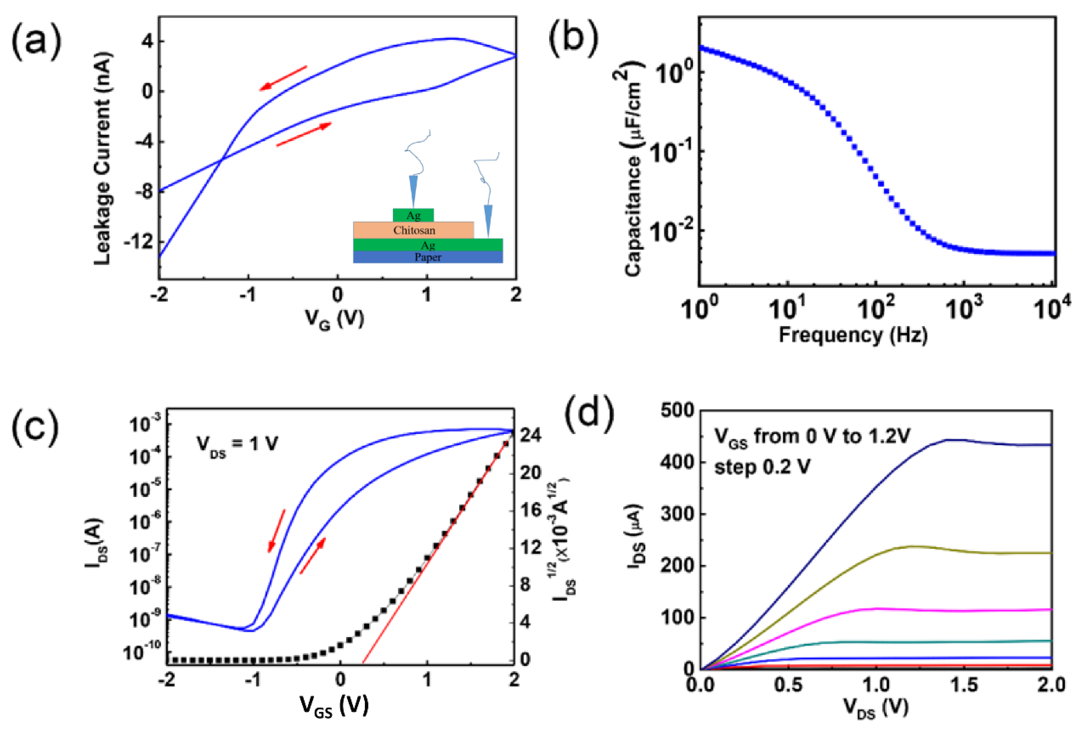
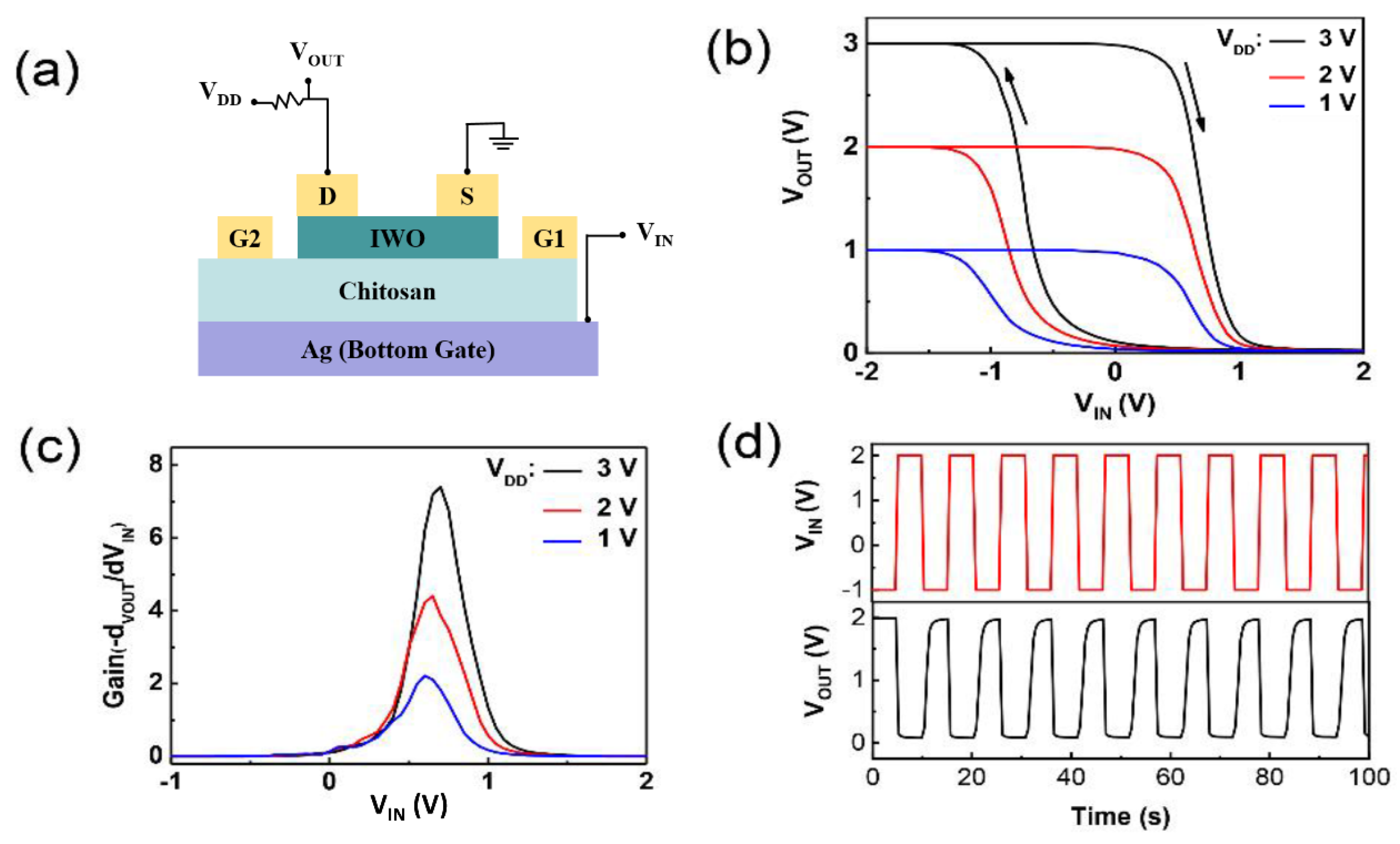
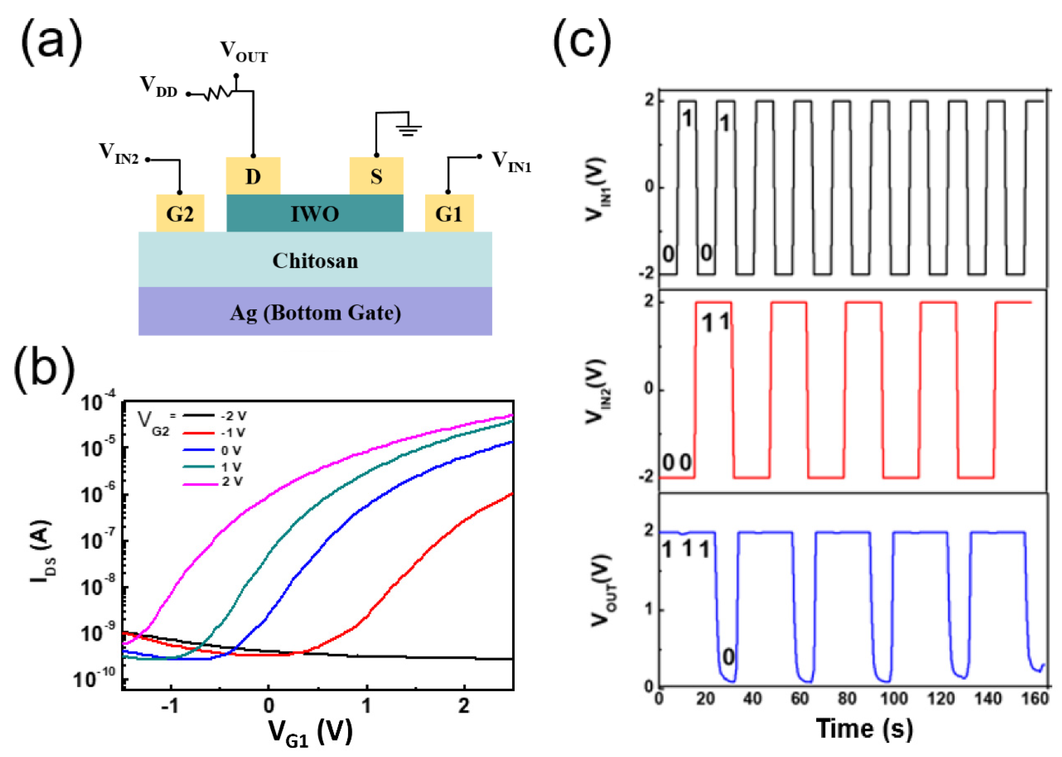
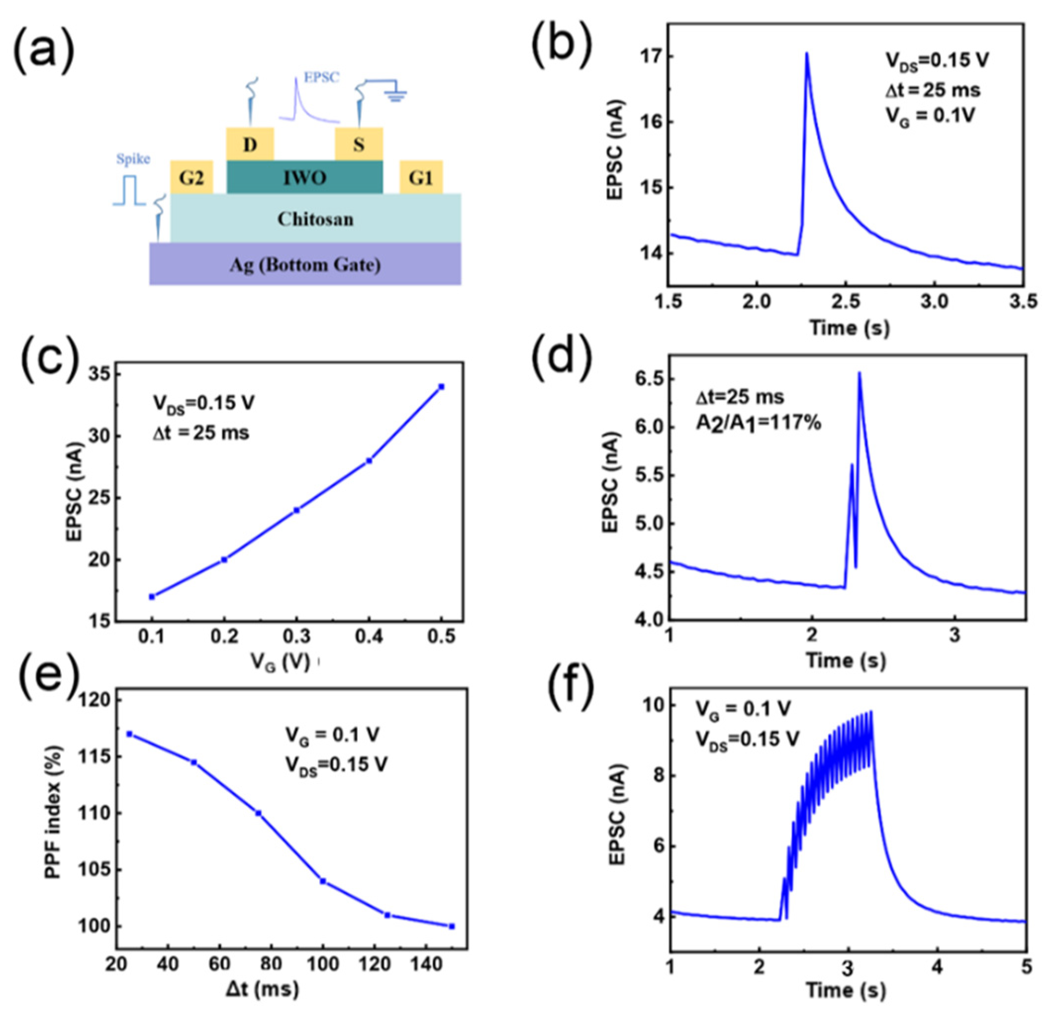
3. Results and Discussion
4. Conclusions
Author Contributions
Funding
Data Availability Statement
Conflicts of Interest
References
- Nomura, K.; Ohta, H.; Takagi, A.; Kamiya, T.; Hirano, M.; Hosono, H. Room-temperature fabrication of transparent flexible thin-film transistors using amorphous oxide semiconductors. Nature 2004, 432, 488–492. [Google Scholar] [CrossRef] [PubMed]
- Ding, X.; Yang, B.; Xu, H.; Qi, J.; Li, X.; Zhang, J. Low-temperature fabrication of IZO thin film for flexible transistors. Nanomaterials 2021, 11, 2552. [Google Scholar] [CrossRef] [PubMed]
- Lee, H.E.; Kim, S.; Ko, J.; Yeom, H.-I.; Byun, C.-W.; Lee, S.H.; Joe, D.J.; Im, T.-H.; Park, S.-H.K.; Lee, K.J. Skin-like oxide thin-film Transistors for transparent displays. Adv. Funct. Mater. 2016, 26, 6170–6178. [Google Scholar] [CrossRef]
- Zhang, Y.; Mei, Z.; Li, J.; Liang, H.; Du, X. Dual-source device architecture for self-diagnosis and correction of gate bias-stress instability in flexible transparent ZnO thin-film transistors. J. Alloys Compd. 2020, 823, 153824. [Google Scholar] [CrossRef]
- Yu, B.; Favela, C.A.; Sun, S.; Sharma, S.; Zhang, C.; Terlier, T.; Chen, J.; Selvamanickam, V. Flexible high-temperature polycrystalline silicon thin film transistor on metal foil with S/D doped by diffusion. IEEE Trans. Electron Devices 2021, 68, 3857–3862. [Google Scholar] [CrossRef]
- Song, D.; Zare Bidoky, F.; Hyun, W.J.; Walker, S.B.; Lewis, J.A.; Frisbie, C.D. All-printed, self-aligned carbon nanotube thin-film transistors on imprinted plastic substrates. ACS Appl. Mater. Interfaces 2018, 10, 15926–15932. [Google Scholar] [CrossRef]
- Nie, S.; Yang, Y.; He, Y.; Shi, Y.; Wan, Q. Flexible IZO homojunction TFTs with graphene oxide/chitosan Composite gate dielectrics on paper substrates. IEEE Electron. Device Lett. 2018, 39, 363–366. [Google Scholar] [CrossRef]
- Cho, K.G.; Cho, Y.K.; Kim, J.H.; Yoo, H.Y.; Hong, K.; Lee, K.H. Thermostable ion gels for high-temperature operation of electrolyte-gated transistors. ACS Appl. Mater. Interfaces 2020, 12, 15464–15471. [Google Scholar] [CrossRef]
- Lu, A.; Sun, J.; Jiang, J.; Wan, Q. Low-voltage transparent electric-double-layer ZnO-based thin-film transistors for portable transparent electronics. Appl. Phys. Lett. 2010, 96, 043114. [Google Scholar] [CrossRef]
- Fortunato, E.; Barquinha, P.; Martins, R. Oxide semiconductor thin-film transistors: A review of recent advances. Adv. Mater. 2012, 24, 2945–2986. [Google Scholar] [CrossRef]
- John, R.A.; Nguyen, A.C.; Chen, Y.X.; Shukla, S.; Chen, S.; Mathews, N. Modulating cationic ratios for high-performance transparent solution-processed electronics. ACS Appl. Mater. Interfaces 2016, 8, 1139–1146. [Google Scholar] [CrossRef] [PubMed]
- Petti, L.; Münzenrieder, N.; Vogt, C.; Faber, H.; Büthe, L.; Cantarella, G.; Bottacchi, F.; Anthopoulos, T.D.; Tröster, G. Metal oxide semiconductor thin-film transistors for flexible electronics. Appl. Phys. Rev. 2016, 3, 021303. [Google Scholar] [CrossRef]
- Liu, P.T.; Chou, Y.T.; Teng, L.F. Environment-dependent metastability of passivation-free indium zinc oxide thin film transistor after gate bias stress. Appl. Phys. Lett. 2009, 95, 233504. [Google Scholar] [CrossRef]
- Park, J.S.; Kim, K.; Park, Y.G.; Mo, Y.G.; Kim, H.D.; Jeong, J.K. Novel ZrInZnO thin-film transistor with excellent stability. Adv. Mater. 2009, 21, 329–333. [Google Scholar] [CrossRef]
- Park, S.; Jang, J.T.; Hwang, Y.; Lee, H.; Choi, W.S.; Kang, D.; Kim, C.; Kim, H.; Kim, D.H. Effect of the gate dielectric layer of flexible InGaZnO synaptic thin-film transistors on learning behavior. ACS Appl. Electron. Mater 2021, 3, 3972–3979. [Google Scholar] [CrossRef]
- Zhang, C.; Li, D.; Lai, P.T.; Huang, X.D. Effects of back interface on performance of dual-gate InGaZnO thin-film transistor with an unisolated top gate structure. IEEE Electron Device Lett. 2021, 42, 1176–1179. [Google Scholar] [CrossRef]
- Felizco, J.C.; Uenuma, M.; Fujii, M.N.; Uraoka, Y. Improved thermoelectric power factor of InGaZnO/SiO2 thin film transistor via gate-tunable energy filtering. IEEE Electron Device Lett. 2021, 42, 1236–1239. [Google Scholar] [CrossRef]
- Chien, Y.T.; Tsai, Y.L.; Zhou, K.J.; Zheng, Y.Z.; Tai, M.C.; Tu, H.Y.; Kuo, C.W.; Chang, T.C.; Tsai, T.-M. Performance enhancement of InGaZnO top-gate thin film transistor with low-temperature high-pressure fluorine treatment. IEEE Electron Device Lett. 2021, 42, 1611–1614. [Google Scholar] [CrossRef]
- Tiwari, N.; Rajput, M.; John, R.A.; Kulkarni, M.R.; Nguyen, A.C.; Mathews, N. Indium tungsten oxide thin films for flexible high-performance transistors and neuromorphic electronics. ACS Appl. Mater. Interfaces 2018, 10, 30506–30513. [Google Scholar] [CrossRef]
- Gao, Y.; Wang, X.; Luo, J.; Liu, Z.; Wan, Q. Schmitt triggers with adjustable hysteresis window based on indium–tungsten-oxide electric-double-layer TFTs. IEEE Electron. Device Lett. 2019, 40, 1205–1208.21. [Google Scholar] [CrossRef]
- Yu, F.; Zhu, L.Q.; Gao, W.T.; Fu, Y.M.; Xiao, H.; Tao, J.; Zhou, J.M. Chitosan-based polysaccharide-gated flexible indium tin oxide synaptic transistor with learning abilities. ACS Appl. Mater. Interfaces 2018, 10, 16881–16886. [Google Scholar] [CrossRef] [PubMed]
- Zhou, B.; Sun, J.; Han, X.; Jiang, J.; Wan, Q. Low-voltage organic/inorganic hybrid transparent thin-film transistors gated by chitosan-based proton conductors. IEEE Electron. Device Lett. 2011, 32, 1549–1551. [Google Scholar] [CrossRef]
- Shao, F.; Wan, X.; Yang, Y.; Du, P.; Feng, P. Optimization of chitosan gated electric double layer transistors by combining nanoparticle incorporation and acid doping. RSC Adv. 2016, 6, 109803–109808. [Google Scholar] [CrossRef]
- Lu, G.; Liu, Y.; Lin, F.; Gen, K.; Wu, W.; Yao, R. Realization of artificial synapse and inverter based on oxide electric-double-layer transistor gated by a chitosan biopolymer electrolyte. Semicond. Sci. Technol. 2020, 35, 075014. [Google Scholar] [CrossRef]
- Ren, Z.Y.; Zhu, L.Q.; Yu, F.; Xiao, H.; Xiong, W.; Ge, Z.Y. Synaptic metaplasticity of protonic/electronic coupled oxide neuromorphic transistor. Org. Electron. 2019, 74, 304–308. [Google Scholar] [CrossRef]
- Wang, W.; He, G.; Wang, L.; Xu, X.; Zhang, Y. Solution-driven HfLaOx-based gate dielectrics for thin film transistors and unipolar inverters. IEEE Trans. Electron Devices 2021, 68, 4437–4443. [Google Scholar] [CrossRef]
- Wang, W.; He, G.; Yu, H.; Gao, Q.; Wang, L.; Xu, X.; Zhang, Y.; Wu, X.; He, B. Enhanced electrical performance and stability of La-doped indium oxide-based thin-film transistors and application explorations. Phys. Status Solidi A 2021, 219, 2100590. [Google Scholar] [CrossRef]
- Wang, X.; Gao, Y.; Liu, Z.; Luo, J.; Wan, Q. Flexible low-voltage IGZO thin-film transistors with polymer electret gate dielectrics on paper substrates. IEEE Electron Device Lett. 2019, 40, 224–227. [Google Scholar] [CrossRef]
- Shao, F.; Yang, Y.; Zhu, L.Q.; Feng, P.; Wan, Q. Oxide-based synaptic transistors gated by sol-gel silica electrolytes. ACS Appl. Mater. Interfaces 2016, 8, 3050–3055. [Google Scholar] [CrossRef]


| Channel Layer | SS [V/Decade] | Mobility [cm2V−1s−1] | Ion/Ioff | Vth [V] | References |
|---|---|---|---|---|---|
| ITO | 0.095 | 3.6 | ~105 | 0.02 | [21] |
| ITO | 0.093 | 5.7 | ~106 | −0.05 | [22] |
| IGZO | - | 3.3 | 5.1 × 10⁵ | 0.57 | [23] |
| ZnO | 0.135 | 7.8 | 105 | 1.00 | [24] |
| ITO | 0.091 | 5.6 | 107 | 0.10 | [25] |
| IWO | 0.117 | 15.0 | 1.3 × 10⁶ | 0.20 | This work |
Publisher’s Note: MDPI stays neutral with regard to jurisdictional claims in published maps and institutional affiliations. |
© 2022 by the authors. Licensee MDPI, Basel, Switzerland. This article is an open access article distributed under the terms and conditions of the Creative Commons Attribution (CC BY) license (https://creativecommons.org/licenses/by/4.0/).
Share and Cite
Jiang, S.; He, G.; Wang, W.; Zhu, M.; Chen, Z.; Gao, Q.; Liu, Y. Ultralow-Thermal-Budget-Driven IWO-Based Thin-Film Transistors and Application Explorations. Nanomaterials 2022, 12, 3243. https://doi.org/10.3390/nano12183243
Jiang S, He G, Wang W, Zhu M, Chen Z, Gao Q, Liu Y. Ultralow-Thermal-Budget-Driven IWO-Based Thin-Film Transistors and Application Explorations. Nanomaterials. 2022; 12(18):3243. https://doi.org/10.3390/nano12183243
Chicago/Turabian StyleJiang, Shanshan, Gang He, Wenhao Wang, Minmin Zhu, Zhengquan Chen, Qian Gao, and Yanmei Liu. 2022. "Ultralow-Thermal-Budget-Driven IWO-Based Thin-Film Transistors and Application Explorations" Nanomaterials 12, no. 18: 3243. https://doi.org/10.3390/nano12183243
APA StyleJiang, S., He, G., Wang, W., Zhu, M., Chen, Z., Gao, Q., & Liu, Y. (2022). Ultralow-Thermal-Budget-Driven IWO-Based Thin-Film Transistors and Application Explorations. Nanomaterials, 12(18), 3243. https://doi.org/10.3390/nano12183243