Article

Bismuth Complex Controlled Morphology Evolution and CuSCN-Induced Transport Improvement Enable Efficient BiI3 Solar Cells

1
Beijing Advanced Innovation Center for Soft Matter Science and Engineering, Beijing University of Chemical Technology, Beijing 100029, China
2
College of Materials Science and Engineering, Beijing University of Chemical Technology, Beijing 100029, China
*
Author to whom correspondence should be addressed.
Nanomaterials 2022, 12(18), 3121; https://doi.org/10.3390/nano12183121
Submission received: 12 August 2022 / Revised: 2 September 2022 / Accepted: 6 September 2022 / Published: 8 September 2022

Abstract

:
Bismuth triiodide (BiI3) is a particularly promising absorber material for inorganic thin-film solar cells due to its merits of nontoxicity and low cost. However, one key factor that limits the efficiency of BiI3 solar cells is the film morphology, which is strongly correlated with the trap states of the BiI3 film. Herein, we report a coordination engineering strategy by using Lewis base dimethyl sulfoxide (DMSO) to induce the formation of a stable BiI3(DMSO)2 complex for controlling the morphology of BiI3 films. Density functional theory calculations further provide a theoretical framework for understanding the interaction of the BiI3(DMSO)2 complex with BiI3. The obtained BiI3(DMSO)2 complex could assist the fabrication of highly uniform and pinhole-free films with preferred crystallographic orientation. This high-quality film enables reduced trap densities, a suppressed charge recombination, and improved carrier mobility. In addition, the use of copper(I) thiocyanate (CuSCN) as a hole transport layer improves the charge transport, enabling the realization of solar cells with a record power conversion efficiency of 1.80% and a champion fill factor of 51.5%. Our work deepens the insights into controlling the morphology of BiI3 thin films through the coordination engineering strategy and paves the way toward further improving the photovoltaic performances of BiI3 solar cells.

1. Introduction

Inorganic metal halide material seems to be one of the most promising light absorbers for low-cost, eco-friendly, next-generation solar cells owing to its superior stability and potentially high efficiency [1,2,3,4]. Bismuth triiodide (BiI3), as a novel light absorber inorganic metal halide material, has attracted great interest due to its low-toxicity, earth-abundance and good optoelectrical properties. The absorption coefficient of BiI3 (>105 cm−1) is competitive with that of Si and metal halide perovskite in the visible region of the solar spectrum [5,6]. In addition, the electron diffusion length and electronic mobility of the BiI3 can reach 4.9 μm and 600 cm2 V−1 s−1, respectively, which are comparable with the properties of typical thin-film materials, such as CdTe [7,8,9,10]. These features indicate that BiI3 is a promising absorber material, and the first BiI3 solar cell was demonstrated in 2015 with a power conversion efficiency (PCE) of 0.3% [11]. Obviously, the efficiency is pretty low and further improvement is greatly needed to solve the challenges that hamper the development of BiI3 solar cells.
One of the most important challenges is the acquisition of high quality BiI3 thin films with appropriate morphology, which is closely related to the optoelectronic properties of BiI3 films. To obtain dense and uniform absorber films for fabricating high-performance BiI3 solar cells, various methodologies have been developed to optimize the morphology of BiI3 thin films. Post-treatment including recycled vapor annealing [12], thermal annealing [13], and solvent vapor annealing [14], and precursor engineering including additive engineering [15], solvent engineering [16], and coordination engineering [17], are feasible methods to promote crystal growth and improve the crystallinity of BiI3 thin films. Coordination engineering has been proven to be an effective strategy in lead-based perovskite solar cells to control the morphology of absorber layers by changing the coordination solvent [18,19,20,21]. Since both Pb and Bi halides can form adducts with most Lewis base solvents, one can utilize a coordination engineering strategy to manipulate the crystallization dynamics and the resulting morphology of BiI3 absorber layers by varying the concentration of Lewis base solvents in precursor solutions to tune the interaction strength between BiI3 and Lewis base solvents. For example, the preferred orientation, aggregate size, and surface coverage of the BiI3 thin film was finely tuned by controlling the mixing ratios of solvent additive with a higher Gutmann donor number [17]. However, a scientific investigation of the status of coordination complexes during the film fabrication process has not been thoroughly conducted, and fundamental mechanisms in the complexes’ formation to manipulate grain nucleation and growth have not been well addressed yet.
In addition, another important challenge is how to construct efficient devices based on the high quality BiI3 thin films. NbSex interlayers were inserted between the poly(3,4-ethylenedioxythiophene)–poly(styrenesulfonate)(PEDOT:PSS) buffer layer and the BiI3 active layer to decrease the interfacial recombination and enhance exciton separation, and the PCE of the device increased from 0.33 to 0.64% [22]. An in situ-generated bismuth sulfide iodide (BiSI) interlayer at the interface of the BiI3 absorber layer and the SnO2 electron transport layer by the reaction of In2S3 and BiI3 at 200 °C were introduced in ITO/SnO2/BiSI/BiI3/Spiro-OMeTAD/Au structured solar cells, and a PCE of 1.21% was achieved due to the improved charge separation [23]. Highly crystalline BiI3 films with a rhombohedral phase and a high-degree of stacking order were obtained through gas-phase iodination of Bi2S3 from thermolysis of Bi(NO3)3 and thiourea precursor. By introducing the polymer hole transport layer (HTL), poly(9,9-di-n-octylfluorenyl-2,7-diyl) (F8), an open-circuit voltage (VOC) of 0.6 V and a PCE of 1.2% were achieved for FTO/TiO2/BiI3/F8/Au-based solar cells [24]. We previously introduced a light-absorbing conjugated polymer for building a BiI3/polymer heterojunction to expand the light harvesting, and the highest short-circuit density (JSC) of 7.8 mA cm−2 was achieved for BiI3-based solar cells with light response to 800 nm [15]. Thus far, the record PCE of 1.5% was achieved for BiI3 solar cells by constructing a binary quasi-bulk heterojunction between a BiI3 electron donor and PC61BM electron acceptor, which effectively promoted the exciton separation [25].
In this work, we report a coordination engineering strategy by introducing a Lewis base dimethyl sulfoxide (DMSO) into the BiI3 precursor solution to form a stable complex BiI3(DMSO)2, which favors control of the crystallization processes of BiI3 and manipulates the morphology of the BiI3 layer. The crystalline structure of BiI3(DMSO)2 was confirmed by single-crystal X-ray diffraction, and further density functional theory (DFT) calculations proved that the formed BiI3(DMSO)2 tends to fill the iodine vacancies, resulting in a strong interaction between the BiI3(DMSO)2 complex and the BiI3 active layer. This high-quality film enables reduced trap densities, suppressed charge recombination, and improved carrier mobility. We further employed copper(I) thiocyanate (CuSCN) as a HTL to fabricate BiI3 solar cells. CuSCN exhibits a chemical compatible and deeper-lying valence band maximum (VBM) with the valence band of BiI3, leading to improved carrier transfer and good Ohmic contact. Benefiting from the high-quality BiI3 film and excellent hole transport of CuSCN, a BiI3 solar cell with a structure of ITO/CuSCN/BiI3/PC71BM/Ca/Al is demonstrated, and a record PCE of 1.80% with a champion fill factor (FF) of 51.5% were achieved.

2. Materials and Methods

2.1. Materials

Indium tin oxide (ITO) glass substrates were purchased from South China Science & Technology Company Limited (Shenzhen, China). Anhydrous bismuth triiodide (BiI3, >98.0%, anhydrous) was purchased from Tci (Shanghai, China). Copper(I) thiocyanate (CuSCN, 99%) was purchased from Aladdin (Shanghai, China). [6,6]-phenyl-C71-butyric acid methyl ester (PC71BM) was purchased from Organtec Ltd (Beijing, China). Diethyl sulfide (DES, 97%+) was purchased from Adamas (Shanghai, China). Tetrahydrofuran (THF, 99.5%, extra dry), dimethyl sulfoxide (DMSO, 99.7+%, extra dry), trichloromethane (CF), and chlorobenzene (CB, 99.8%, extra dry) were purchased from Acros (Geel, Belgium). All of the materials were used as received without further purification.

2.2. Preparation of Precursor Solution

For the BiI3 solution, 120 mg/mL BiI3 solution was prepared by dissolving BiI3 in THF. The Lewis base solvent DMSO was added to the THF in the following volume ratios: 0%, 0.3%, 0.5%, and 0.7%. For the CuSCN solution, 25 mg/mL CuSCN solution was prepared by dissolving CuSCN in DES. The BiI3 solution and the CuSCN solution were stirred at 1000 rpm overnight at room temperature. Afterwards, the BiI3 solution and the CuSCN solution were filtered with a 0.22 µm PTFE filter and 0.2 µm PVDF filter, respectively. For the PC71BM solution, 15 mg/mL PC71BM solution was prepared by dissolving PC71BM in CB. The PC71BM solution was stirred at 800 rpm overnight at 40 °C.

2.3. Device Fabrication

ITO glass substrates were cleaned with detergent, water, ultrapure water, and ethanol for 15 min in an ultrasonicator, respectively. Next, the substrates were treated with UV-ozone for 15 min before use. Then, the CuSCN thin films were deposited as HTL by spin-coating at 3500 rpm for 60 s and were annealed at 100 °C for 10 min. The BiI3 solution with or w/o DMSO was coated by spin-coating on the CuSCN substrates at 3000 rpm for 30 s; 150 µL of CF was dropped on the spinning substrate 20 s prior to the end of the program. Afterward, the substrates were transferred onto a hotplate and heated at 100 °C for 10 min. After the substrates cooled down to room temperature, a PC71BM solution was spin-coated at 1300 rpm for 60 s. Then the substrates were heated at 100 °C for 10 min. Finally, 20 nm Ca and 100 nm Al was deposited on the ETM surface by thermal evaporation.

2.4. Characterization

Ruby-red crystals of BiI3(DMSO)2 were prepared by means of the previously reported anti-solvent vapor-assisted crystallization approach [26], using 1.0 mL of a saturated DMSO solution of BiI3 with CHCl3 as the anti-solvent. The crystal structure of BiI3(DMSO)2 was characterized by single-crystal X-ray diffraction (Rigaku XtalAB PRO MM007DW, Tokyo, Japan). Direct methods and SHELXTL program were employed to solve and refine the crystal structure. The chemical composition of BiI3 films was analyzed applying X-ray photoelectron spectroscopy (XPS, Kratos AXIS ULTRA DLD, Kyoto, Japan). A Fourier transform infrared spectroscopy (FTIR, Nicolet 8700, Thermo Electron Corporation, Waltham, MA, USA) was employed to obtain the FTIR spectral data for DMSO (liquid phase) and bismuth complexes. The crystal structures of the formed BiI3 films were characterized by performing X-ray powder diffractometer (XRD-6000, SHIMADZU, Kyoto, Japan). Thermogravimetric analysis (TGA) was performed using a TA Instruments TGAQ500 (New Castle, PA, USA) with a ramp of 10 °C min–1 under N2 from 30 to 800 °C. A UV–Vis–NIR 3600 spectrometer (SHIMADZU, Kyoto, Japan) was performed to obtain UV–Vis spectroscopy. The morphology of BiI3 films was characterized by conducting scanning electron microscopy (SEM, HITACHI S-470, Tokyo, Japan) and atomic force microscope (AFM, Bruker DMFASTSCAN2-SYS, Karlsruhe, Germany). The electronic properties of bismuth complex and CuSCN HTL films were characterized by ultraviolet photoemission spectroscopy (UPS, Kratos AXIS ULTRA DLD, He−Iα = 21.22 Ev, Kyoto, Japan). The JV characteristics were measured under the illumination with a solar simulator (SS-F5-3A, EnliTech, Kaohsiung City, Taiwan) at an intensity 100 mW/cm2 in N2 atmosphere. The EQE measurements were performed using QE-R systems (EnliTech, Kaohsiung City, Taiwan) in ambient atmosphere.

2.5. Computational Methods

The DFT calculations were performed with PAW pseudopotential method as implemented in the Vienna Ab Initio Simulation Package (VASP) [27,28]. The Perdew–Burke–Ernzerhof (PBE) functional within the generalized gradient approximation (GGA) exchange correlation was utilized [29]. The vdW correction of Grimmer’s DFT+D3 was included in all calculations [30,31] because the vdW correction plays an important role in describing the weak interactions within perovskite material. The plane wave cutoff was set to 400 eV for the adsorption of BiI3 (DMSO)2 on the BiI3 surfaces. The 1 × 1 × 1 k-point mesh was used to optimize the structure in the 3 × 3 supercell. In all calculations, the value of vacuum space is about 15 Å along the z direction to eliminate the image interaction, and the structures were relaxed until the maximum atomic force was less than 0.01 eV·Å−1. The energy difference of these structures was within 10−5 eV. The adsorption energies of BiI3 (DMSO)2 on the surface of BiI3 were calculated as follows
Eads = E(BiI3 + complex) − E(complex) − E(BiI3)
where E(BiI3 + complex) represents the total energy of the BiI3(DMSO)2 complex on the BiI3 substrates, E(BiI3) is the energy of the BiI3 substrates, and E(complex) is the energy of the BiI3(DMSO)2 complex.

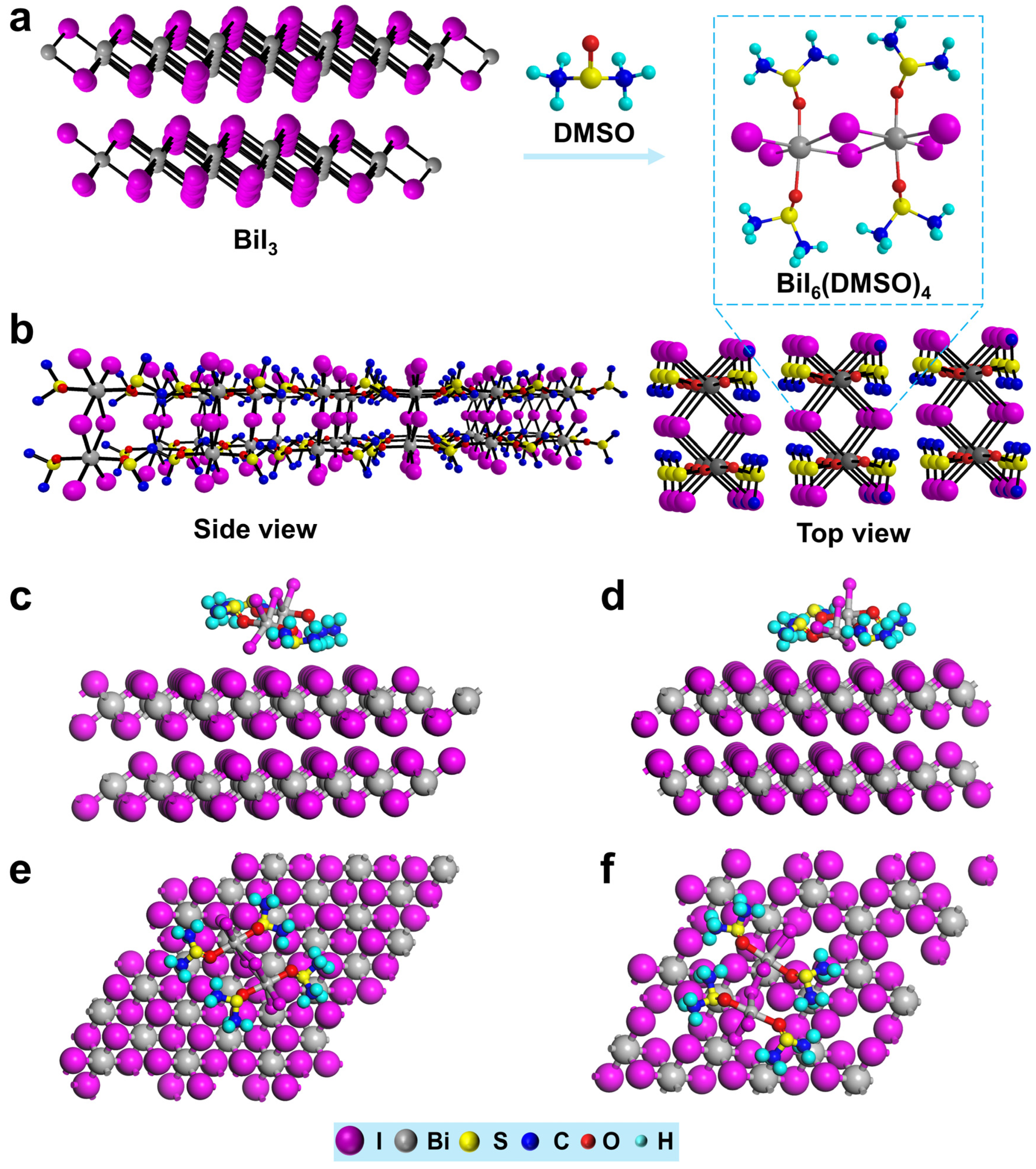
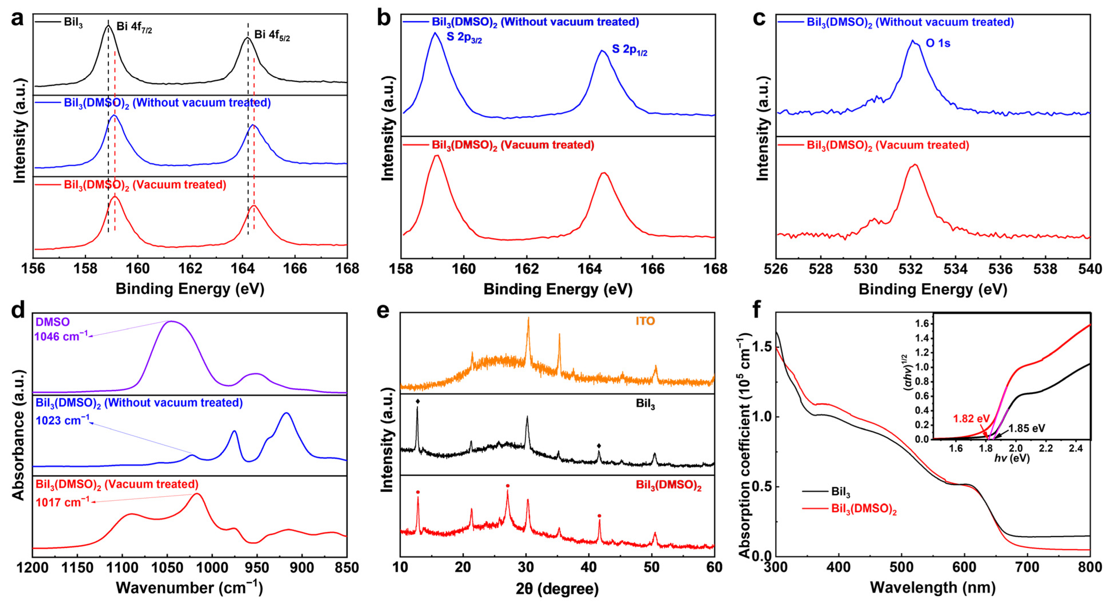
3. Results and Discussion

Figure 1a shows the crystals of BiI3(DMSO)2, which can be obtained by the coordination engineering strategy of introducing Lewis base DMSO into the BiI3 precursor solution followed by an anti-solvent vapor-assisted crystallization approach [26]. Figure 1b gives the crystal structure of BiI3(DMSO)2, which is further confirmed by single-crystal X-ray diffraction and the structural details are listed in Table S1. The incorporation of a DMSO ligand changes the coordination state of BiI3. The boxed fragment can be described as a symmetric complex (Bi2I6(DMSO)4) with an edge-shared and bi-octahedral crystal structure. Six iodide ions occupy the corners of the bi-octahedral, while the Bi ions at the body center and the O-coordinated DMSO molecules complete the coordination structure.
To gain insight into the interaction between the BiI3(DMSO)2 complex and BiI3 surfaces, first-principles DFT calculations were carried out (the procedure is outlined in the Experimental Section in the Supporting Information). The optimized structures of BiI3(DMSO)2 absorbing on the BiI3 surfaces are shown in Figure 1c–f. In order to visualize the adsorption structure, only the upper adsorption structures are presented. The adsorption energy of BiI3(DMSO)2 on the BiI3 is −1.08 eV. Structural defects are often the most important factor affecting the performance of solar cell materials, so a full understanding of the defect is of great importance. The iodide vacancy defect was introduced to BiI3 surfaces due to its low formation energy. Comparing the perfect BiI3 surfaces, the adsorption energy of the BiI3(DMSO)2 complex on defective BiI3 surfaces changes to −1.83 eV, which suggests a stronger adsorption on the defective BiI3 surfaces than the perfect case. When iodide vacancies within BiI3 surfaces are created, the iodine element in the BiI3(DMSO)2 complex tends to fill the iodine vacancies, resulting in a significant interaction between the BiI3(DMSO)2 complex and the defective BiI3 surfaces. Overall, our theoretical calculation results confirm that the adsorption of the BiI3(DMSO)2 complex successfully passivates the BiI3 film to modulate its surfaces’ properties.
To deeply understand the bonding interactions between BiI3 and DMSO, the X-ray photoelectron spectroscopy (XPS) characterizations were performed. The survey scans of BiI3 and DMSO-coordinated BiI3 are shown in Figure S1. The core level scans of Bi 4f for each sample are compared (Figure 2a). For the BiI3 film, two main peaks located at 164.2 and 158.9 eV are observed, which are assigned to Bi 4f5/2 and Bi 4f7/2, respectively. However, in the DMSO-coordinated sample, the peaks of Bi 4f shift to a higher binding energy compared to that of BiI3 film, attributed to the formation of coordination bonds between Bi from the BiI3 and O from DMSO. More importantly, it can be seen that no significant shift in the Bi 4f core level is observed after vacuum treatment for the DMSO-coordinated BiI3 film under a pressure of 5 × 10⁻⁵ Pa for 1 h. In addition, the existence of S and O is proved by the evident signals of S 2p at 159.1 and 164.4 eV and O 1s at 532.2 eV (Figure 2b,c). The stability of the BiI3(DMSO)2 complex was further confirmed by TGA measurement. The TGA curves in Figure S2 revealed that the BiI3(DMSO)2 complex was thermally stable up to 190 °C. These results confirm that BiI3(DMSO)2 acts as a stable complex rather than an intermediate adduct phase.
The coordination interaction was further confirmed by Fourier transform infrared spectroscopy (FTIR). As shown in Figure 2d, the stretching vibration of S=O (ν(S=O)) appears at 1046 cm−1 for the pure DMSO, which is shifted to 1023 cm−1 upon formation of the BiI3(DMSO)2 complex [20,32,33]. According to the diatomic harmonic model, the square root of the force constant is proportional to the frequency of vibration [34]. Based on this model, the decreased S=O stretching vibration frequency denotes that the force constant is reduced, which is ascribed to the decreased strength of the S=O bond as a consequence of BiI3(DMSO)2 complex formation. Therefore, the S=O stretching vibration frequency of BiI3(DMSO)2 is detected in a lower wavenumber than that of DMSO. Additionally, the stretching vibration frequency of S=O does not shift after vacuum treatment, indicating the strong interaction between BiI3 and DMSO, which is consistent with the observation from XPS.
The effects of the BiI3(DMSO)2 complex on the crystallographic structure and optical properties of BiI3 films were further investigated. The X-ray diffraction (XRD) patterns of BiI3 films processed in different conditions are shown in Figure 2e. The BiI3 film processed without DMSO exhibits two diffraction peaks at 2-Theta of 12.8° and 41.6°, which are in good accordance with previous work [14]. Notably, in the DMSO-coordinated BiI3 film, a signature peak at 26.9° appears, indicating the preferred orientation of the BiI3(DMSO)2 complex on the (113) lattice plane. It can be concluded that the DMSO-coordinated BiI3 thin film is composed of the BiI3(DMSO)2 complex and BiI3 from the results of XPS and XRD spectra. This is completely consistent with the DFT calculation. UV−Vis absorption spectra (Figure 2f) were measured to evaluate the effect of the formation of the BiI3(DMSO)2 complex on the optical properties of BiI3 films. The absorption of BiI3 film in the wavelength region from 300 to 650 nm is slightly enhanced with the addition of DMSO, and Tauc analysis of the absorption spectra reveals a slightly decreased band gap from 1.85 to 1.82 eV for the DMSO-coordinated BiI3 film (Figure 2f, inset). These results suggest that the formation of BiI3(DMSO)2 can significantly affect the crystallization kinetics of BiI3 and change the optoelectronic properties of the thin film.
In order to further understand the influences of DMSO concentrations and CF anti-solvent treatment on the crystallization process and relevant thin film morphology, top-view scanning electron microscopy (SEM) and atomic force microscopy (AFM) measurements on the corresponding BiI3 thin films were conducted. As shown in Figure 3a, the as-cast BiI3 film without DMSO exhibits incomplete surface coverage and is composed of rod-like BiI3 crystals, which can be ascribed to a relatively fast crystal growth rate during the spin-coating process. After adding 0.3% DMSO, the uniformity of BiI3 film is significantly improved, while there exists some small void spaces (Figure 3b). As depicted in Figure 3c, the 0.5% DMSO-coordinated film shows a compact and uniform morphology. These could be attributed to the fact that the BiI3(DMSO)2 complex controls nucleation, retards the crystal growth, and then assists the formation of a highly uniform morphology. When the content of DMSO further increases to 0.7%, some pinholes appear, while most regions of the film are still quite dense (Figure 3d). Interestingly, when we used CF as the anti-solvent, the quality of the obtained film was significantly improved compared with that of the film without dropping anti-solvent. It can be seen from Figure 3i–l that a dense and uniform BiI3 film morphology can be obtained after CF anti-solvent treatment. The control BiI3 film shows a smooth morphology with an apparent grain boundary, while the DMSO-coordinated one displays an increased crystal domain size and more uniform size distribution than the control sample. The uniformity and compactness further increase at higher DMSO loading. The influences of DMSO concentrations and CF anti-solvent treatment on the BiI3 surface roughness were monitored by AFM (Figure 3e–h,m–p). The crystal domain size increases after the introduction of DMSO coordinative solvent and CF anti-solvent. This is consistent with the results obtained from SEM. The measured root-mean-square roughness values of the control film and DMSO-coordinated BiI3 film with CF anti-solvent are 15.0 nm and 18.1 nm, respectively. The larger and more uniform crystal grain size of the thin film suggests reduced defects as well as nonradiative recombination centers. These results demonstrated that the utilization of CF as an anti-solvent and DMSO as a coordinative solvent successfully assist the formation of a uniform and compact absorber layer.
Based on the obtained high quality BiI3 thin films, p–i–n structured planar heterojunction solar cells were designed and fabricated (Figure 4a). For this structure, PEDOT:PSS is the most commonly used HTL [13,22,25]. However, the PEDOT:PSS exhibits a shallow VBM, which is a mismatch with the deep-lying valence band of BiI3. Considering the energetic alignment theory, the HTL should have a relatively deep VBM to match with that of the BiI3 absorber layer. Fortunately, inorganic CuSCN with a deeper lying VBM can perfectly meet this demand as the HTL, and the good alignment with the BiI3 film can greatly enhance the hole extraction. The energy levels of CuSCN and BiI3 films were determined from ultraviolet photoelectron spectroscopy (UPS) and optical measurements of the band gap (Figures S3 and S4). Figure 4b gives the energy level diagram of the device with the structure of ITO/CuSCN/BiI3/PC71BM/Ca/Al (Figure 4a). The valence band edge for CuSCN is 6.12 eV, which is close to that of the BiI3 film (6.55 eV) and DMSO-coordinated BiI3 film (6.42 eV). However, for PEDOT:PSS with a HOMO level of 5.0 eV, there is a large barrier of over 1.42 eV to the photoactive layer of BiI3 and DMSO-coordinated BiI3 films. Obviously, more favorable energetics alignment with a CuSCN HTL can be achieved in comparison to PEDOT:PSS-based devices.
For comparison, BiI3-based solar cells with CuSCN or PEDOT:PSS as the HTL and BiI3 or DMSO-coordinated BiI3 as the photoactive layer were fabricated. Figure 4c gives the current density–voltage (JV) curves of the corresponding devices under AM 1.5 G (100 mW/cm2) illumination, and the photovoltaic parameters of the champion devices are summarized in Table 1. The PEDOT:PSS-based device with a BiI3 photoactive layer shows a VOC of 0.40 V, an FF of 46.8%, a JSC of 2.54 mA/cm2 and a PCE of 0.48%. By using DMSO-coordinated BiI3 as the photoactive layer, all the photovoltaic parameters are increased, achieving a PCE of 0.81%, with an FF of 48.6%, a VOC of 0.49 V, and a JSC of 3.43 mA/cm2. Moreover, introducing CuSCN as the HTL and BiI3 as the photoactive layer, the device shows a PCE of 0.80%, with a VOC of 0.47 V, an FF of 45.9%, and a JSC of 3.68 mA/cm2. Further employing DMSO-coordinated BiI3 as the photoactive layer, all photovoltaic parameters can be simultaneously improved and the best PCE of 1.80% can be achieved, with an FF of 51.5%, a VOC of 0.55 V, and a JSC of 6.38 mA/cm2. Compared with previous reports, the achieved PCE of 1.80% and FF of 51.5% are the highest values reported for BiI3 solar cells (Figure S5 and Table S2), which is related to the device structure and morphology of BiI3 thin films [11,12,13,14,15,16,17,22,23,24,25,35]. Haque et al. used SnO2 to fabricate n-i-p BiI3 solar cells, which resulted in a JSC of up to 12.6 mA/cm2 and PCE of 1.21%; however, the FF remained limited to 29.0% [23]. Conducting polymers such as polytriarylamine (PTAA) has been employed as an HTL [13]. The HTL can improve the VOC but at the cost of the JSC. CuSCN in our devices can improve the charge transfer and the BiI3(DMSO)2 complex can control the quality of BiI3 films. Notably, our champion BiI3 solar cell reached a relatively higher PCE in Bi-based solar cells (Table S3) [36,37,38,39,40,41]. Figure 4d displays the external quantum efficiency (EQE) spectra of the corresponding devices, and the integrated JSC is in good agreement with the J–V curve-derived JSC, showing the strong reliability of the tested results. We notice that the VOC values of CuSCN-based devices are higher than those of their PEDOT:PSS-based counterparts due to the better VBM alignment of the CuSCN HTL with the BiI3 photoactive layer (Figure 4b). To verify the reproducibility, a batch of 30 devices with a CuSCN HTL and BiI3 or DMSO-coordinated BiI3 photoactive layers was fabricated. The statistical photovoltaic parameters of VOC, JSC, FF, and PCE are given in Figure S6, and their performance features are summarized in Table S4. DMSO-coordinated BiI3-based devices show a narrow distribution with a high PCE of 1.75 (±0.02)%.
To further understand the enhanced JSC and FF for devices based on the DMSO-coordinated BiI3 photoactive layer, the light intensity-dependent JSC and VOC for both devices with BiI3 and DMSO-coordinated BiI3 were tested to investigate the charge recombination processes [42]. The JSC versus light intensity (Plight) follows the relationship of ln ( J S C ) α ln ( P l i g h t ) , and the slop α reflects the charge recombination in the devices. As shown in Figure 5a, the device based on the DMSO-coordinated BiI3 film shows a slope of 0.982, while the control device with BiI3 film shows a smaller slope of 0.917. The larger slope for the DMSO-coordinated device indicates that the carrier recombination is suppressed, and the charge accumulation within the devices is prevented [43]. Figure 5b shows the relationship between VOC and Plight, which follows the relationship of V O C N ( K B T / q ) ln ( P l i g h t ) [44], where q is the elementary charge, KB is the Boltzmann constant, and T is the temperature, and the charge recombination process is reflected by the ideality factor N. In general, the value of N approaches unity for ideal photovoltaic devices. However, when the value of N approaches 2, the Shockley−Read−Hall (SRH) recombination assisted by trap density dominates [45]. It can be seen that the N for the control device with the BiI3 layer is 1.40, while the device with the DMSO-coordinated BiI3 layer shows a smaller N of 1.12, indicating that the trap-assisted SRH recombination is effectively suppressed, and the inherent trap density is reduced.
The dark current characteristics of BiI3 solar cells were measured to analyze the loss of the charge carrier via the leakage pathways and charge carrier recombination [46], and the related JV curves are depicted in Figure 5c. The dark current significantly decreases in the DMSO-coordinated BiI3 device, denoting more charge carriers sweep through the device instead of shunting [47]. The decreased leakage current and suppressed carrier recombination result in the improvement in JSC and FF. Furthermore, the electron-only and hole-only devices (inset of Figure 5d,e) based on BiI3 and DMSO-coordinated BiI3 films were fabricated, and the hole and electron mobilities were calculated through the space-charge-limited current (SCLC) method [48]. The BiI3-based device gives a hole mobility of 3.98 × 10⁻⁵ cm2/Vs and electron mobility of 9.97 × 10⁻⁵ cm2/Vs. Contrastively, the DMSO-coordinated BiI3 device demonstrates much higher and more balanced hole and electron mobilities of 2.11 × 10⁻⁴ cm2/Vs and 2.90 × 10⁻⁴ cm2/Vs, respectively, which contribute to the enhancement of FF and JSC.
To confirm the effect of the bismuth complex on the trap states within the BiI3 film, we estimated the trap density of BiI3 film by measuring dark current–voltage characteristics of the hole-only device, where the bias voltage determined as the trap-filled limited voltage (VTFL) is closely related with the trap density [49,50]. As given in Figure 5f, the measured VTFL for the BiI3-based device is ~0.91 V, while the value decreased to 0.67 V for the DMSO-coordinated BiI3 device. The calculated trap density for the BiI3 film is 1.68 × 1017 cm–3 and for the DMSO-coordinated BiI3 film is 1.23 × 1017 cm–3. The reduced trap density in the DMSO-coordinated BiI3 film can effectively suppress the nonradiative recombination, resulting in an improved FF [51,52].

4. Conclusions

In conclusion, we successfully demonstrate efficient BiI3 solar cells by controlling BiI3 film morphology via a stable BiI3(DMSO)2 complex and introducing CuSCN as the HTL for transport improvement. DFT calculation reveals that BiI3(DMSO)2 can fill the iodide vacancies in the BiI3 film to modulate its surface properties. The obtained BiI3(DMSO)2 could trigger homogeneous nucleation and enable a slow crystal growth rate, inducing the formation of highly uniform and pinhole-free BiI3 films with preferred crystallographic orientation and enhanced optical absorption. This high-quality film enables reduced trap densities, suppressed charge recombination, and improved carrier mobility. Furthermore, a deeper lying VBM of the CuSCN HTL ensures Ohmic contact and good charge transport with the BiI3 layer. Overall, a record PCE of 1.80% with a champion FF of 51.5% were achieved for BiI3 solar cells.

Supplementary Materials

The following supporting information can be downloaded at: https://www.mdpi.com/article/10.3390/nano12183121/s1, Figure S1: XPS spectra for BiI3 film, and the DMSO-coordinated BiI3 film without and with vacuum treatment; Figure S2: Thermogravimetric analysis of BiI3(DMSO)2 at (scan rate: 10 °C min−1); Figure S3: UPS spectra of (a,c,e) the high-binding energy secondary electron cutoff regions and (b,d,f) the valence band edge regions of BiI3 film with and w/o DMSO-treated and CuSCN film, respectively; Figure S4: UV−Vis absorption spectra of CuSCN; Figure S5: Comparison of PCE and FF values of this work with previous reported BiI3 photovoltaic devices; Figure S6: Statistical photovoltaic parameters obtained from 30 photovoltaic devices with CuSCN HTL and BiI3 or DMSO-coordinated BiI3 photoactive layers; Table S1: Crystal data and structure refinement for BiI3(DMSO)2 at 298 K; Table S2: Photovoltaic parameters of reported BiI3 solar cells; Table S3. Photovoltaic parameters of reported Bi-based solar cells; Table S4: Photovoltaic parameters of 30 photovoltaic devices with CuSCN HTL and BiI3 or DMSO-coordinated BiI3 photoactive layers.

Author Contributions

Conceptualization, Z.T.; methodology, Z.H.; validation, Z.T.; formal analysis, Z.H.; investigation, Z.H.; resources, Z.T.; data curation, Z.H.; visualization, Z.H.; funding acquisition, Z.T. and R.Y.; project administration, Z.T.; supervision, Z.T.; writing—original draft preparation, Z.H.; software, W.S. and H.L.; writing—review and editing, R.Y. and Y.G. All authors have read and agreed to the published version of the manuscript.

Funding

This work was supported by the National Key Research and Development Program of China (2019YFE0112200), the National Natural Science Foundation of China (51873007, 21835006, 51961165102, and 52003022), the Fundamental Research Funds for the Central Universities of China (PT2021-02, buctrc202009), and the high-performance computing platform of BUCT.

Data Availability Statement

The data presented in this study are available on request from the corresponding author.

Conflicts of Interest

The authors declare no conflict of interest.

References

  1. Liu, C.; Li, W.; Zhang, C.; Ma, Y.; Fan, J.; Mai, Y. All-Inorganic CsPbI2Br Perovskite Solar Cells with High Efficiency Exceeding 13%. J. Am. Chem. Soc. 2018, 140, 3825–3828. [Google Scholar] [CrossRef] [PubMed]
  2. Tian, J.; Xue, Q.; Yao, Q.; Li, N.; Brabec, C.J.; Yip, H.-L. Inorganic Halide Perovskite Solar Cells: Progress and Challenges. Adv. Energy Mater. 2020, 10, 2000183. [Google Scholar] [CrossRef]
  3. Tai, Q.; Tang, K.-C.; Yan, F. Recent progress of inorganic perovskite solar cells. Energy Environ. Sci. 2019, 12, 2375–2405. [Google Scholar]
  4. Li, Y.; Na, G.; Luo, S.; He, X.; Zhang, L. Structural, Thermodynamical and Electronic Properties of All-Inorganic Lead Halide Perovskites. Acta Phys. Chim. Sin. 2020, 37, 2007015. [Google Scholar] [CrossRef]
  5. Green, M.A.; Keevers, M.J. Optical properties of intrinsic silicon at 300 K. Prog. Photovolt. Res. Appl. 1995, 3, 189–192. [Google Scholar] [CrossRef]
  6. Lee, J.-W.; Seol, D.-J.; Cho, A.-N.; Park, N.-G. High-Efficiency Perovskite Solar Cells Based on the Black Polymorph of HC(NH2)2PbI3. Adv. Mater. 2014, 26, 4991–4998. [Google Scholar] [CrossRef]
  7. Han, H.; Hong, M.; Gokhale, S.; Sinnott, S.; Jordan, K.; Baciak, J.; Nino, J. Defect Engineering of BiI3 Single Crystals: Enhanced Electrical and Radiation Performance for Room Temperature Gamma-Ray Detection. J. Phys. Chem. C 2014, 118, 3244–3250. [Google Scholar] [CrossRef]
  8. Lintereur, A.T.; Qiu, W.; Nino, J.C.; Baciak, J. Characterization of bismuth tri-Iodide single crystals for wide band-Gap semiconductor radiation detectors. Nucl. Instrum. Methods Phys. Res. Sect. A Accel. Spectrometers Detect. Assoc. Equip. 2011, 652, 166–169. [Google Scholar] [CrossRef]
  9. Brandt, R.E.; Kurchin, R.C.; Hoye, R.L.Z.; Poindexter, J.R.; Wilson, M.W.B.; Sulekar, S.; Lenahan, F.; Yen, P.X.T.; Stevanović, V.; Nino, J.C.; et al. Investigation of Bismuth Triiodide (BiI3) for Photovoltaic Applications. J. Phys. Chem. Lett. 2015, 6, 4297–4302. [Google Scholar] [CrossRef]
  10. Gumaste, M.R.; Kulkarni, G.A. High mobility and size dependent carrier concentration in CdTe nanoparticles synthesized by single injection hydrothermal method for device applications. Mater. Today Proc. 2021, 45, 3927–3930. [Google Scholar] [CrossRef]
  11. Lehner, A.J.; Wang, H.; Fabini, D.H.; Liman, C.D.; Hébert, C.-A.; Perry, E.E.; Wang, M.; Bazan, G.C.; Chabinyc, M.L.; Seshadri, R. Electronic structure and photovoltaic application of BiI3. Appl. Phys. Lett. 2015, 107, 131109. [Google Scholar] [CrossRef] [Green Version]
  12. Kulkarni, A.; Singh, T.; Jena, A.K.; Pinpithak, P.; Ikegami, M.; Miyasaka, T. Vapor Annealing Controlled Crystal Growth and Photovoltaic Performance of Bismuth Triiodide Embedded in Mesostructured Configurations. ACS Appl. Mater. Inter. 2018, 10, 9547–9554. [Google Scholar] [CrossRef] [PubMed]
  13. Pandian, M.G.M.; Khadka, D.B.; Shirai, Y.; Umedov, S.; Yanagida, M.; Subashchandran, S.; Grigorieva, A.; Miyano, K. Effect of solvent vapour annealing on bismuth triiodide film for photovoltaic applications and its optoelectronic properties. J. Mater. Chem. C 2020, 8, 12173–12180. [Google Scholar] [CrossRef]
  14. Hamdeh, U.H.; Nelson, R.D.; Ryan, B.J.; Bhattacharjee, U.; Petrich, J.W.; Panthani, M.G. Solution-Processed BiI3 Thin Films for Photovoltaic Applications: Improved Carrier Collection via Solvent Annealing. Chem. Mater. 2016, 28, 6567–6574. [Google Scholar] [CrossRef]
  15. Ma, S.; Yang, Y.; Liu, C.; Cai, M.; Ding, Y.; Tan, Z.A.; Shi, P.; Dai, S.; Alsaedi, A.; Hayat, T. Vertically Oriented BiI3 Template Featured BiI3/Polymer Heterojunction for High Photocurrent and Long-Term Stable Solar Cells. ACS Appl. Mater. Inter. 2019, 11, 32509–32516. [Google Scholar] [CrossRef]
  16. Wang, Y.; Shi, X.; Wang, G.; Tong, J.; Pan, D. All-Inorganic and lead-Free BiI3 thin film solar cells by iodization of BiSI thin films. J. Mater. Chem. C 2020, 8, 14066–14074. [Google Scholar] [CrossRef]
  17. Hamdeh, U.H.; Nelson, R.D.; Ryan, B.J.; Panthani, M.G. Effects of Solvent Coordination Strength on the Morphology of Solution-Processed BiI3 Thin Films. J. Phys. Chem. C 2019, 123, 13394–13400. [Google Scholar] [CrossRef]
  18. Ahn, N.; Son, D.Y.; Jang, I.H.; Kang, S.M.; Choi, M.; Park, N.G. Highly Reproducible Perovskite Solar Cells with Average Efficiency of 18.3% and Best Efficiency of 19.7% Fabricated via Lewis Base Adduct of Lead(II) Iodide. J. Am. Chem. Soc. 2015, 137, 8696–8699. [Google Scholar] [CrossRef]
  19. Lee, J.-W.; Dai, Z.; Lee, C.; Lee, H.M.; Han, T.-H.; De Marco, N.; Lin, O.; Choi, C.S.; Dunn, B.; Koh, J.; et al. Tuning Molecular Interactions for Highly Reproducible and Efficient Formamidinium Perovskite Solar Cells via Adduct Approach. J. Am. Chem. Soc. 2018, 140, 6317–6324. [Google Scholar] [CrossRef]
  20. Lee, J.-W.; Kim, H.-S.; Park, N.-G. Lewis Acid-Base Adduct Approach for High Efficiency Perovskite Solar Cells. Acc. Chem. Res. 2016, 49, 311–319. [Google Scholar] [CrossRef]
  21. Zhang, X.; Han, D.; Chen, X.; Chen, Y.; Chang, S.; Zhong, H. Effects of Solvent Coordination on Perovskite Crystallization. Acta Phys. Chim. Sin. 2021, 37, 2008055. [Google Scholar] [CrossRef]
  22. Lin, L.; Boopathi, K.M.; Ding, J.; Chu, C.W.; Chang, C.C. NbSex interlayers decrease interfacial recombination in BiI3-Based hybrid solar cells. FlatChem 2017, 5, 18–24. [Google Scholar] [CrossRef]
  23. Yoo, B.; Ding, D.; Marin-Beloqui, J.M.; Lanzetta, L.; Bu, X.; Rath, T.; Haque, S.A. Improved Charge Separation and Photovoltaic Performance of BiI3 Absorber Layers by Use of an In Situ Formed BiSI Interlayer. ACS Appl. Energy Mater. 2019, 2, 7056–7061. [Google Scholar] [CrossRef]
  24. Tiwari, D.; Alibhai, D.; Fermin, D.J. Above 600 mV Open-Circuit Voltage BiI3 Solar Cells. ACS Energy Lett. 2018, 3, 1882–1886. [Google Scholar] [CrossRef]
  25. Kang, J.; Chen, S.; Zhao, X.; Yin, H.; Zhang, W.; Al-Mamun, M.; Liu, P.; Wang, Y.; Zhao, H. An inverted BiI3/PCBM binary quasi-Bulk heterojunction solar cell with a power conversion efficiency of 1.50%. Nano Energy 2020, 73, 104799. [Google Scholar] [CrossRef]
  26. Shi, D.; Adinolfi, V.; Comin, R.; Yuan, M.; Alarousu, E.; Buin, A.; Chen, Y.; Hoogland, S.; Rothenberger, A.; Katsiev, K.; et al. Low trap-State density and long carrier diffusion in organolead trihalide perovskite single crystals. Science 2015, 347, 519–522. [Google Scholar] [CrossRef]
  27. Kresse, G.; Furthmüller, J. Efficiency of ab-Initio total energy calculations for metals and semiconductors using a plane-Wave basis set. Comput. Mater. Sci. 1996, 6, 15–50. [Google Scholar] [CrossRef]
  28. Kresse, G.; Furthmüller, J. Efficient iterative schemes for ab initio total-Energy calculations using a plane-Wave basis set. Phys. Rev. B 1996, 54, 11169–11186. [Google Scholar] [CrossRef]
  29. Perdew, J.P.; Burke, K.; Ernzerhof, M. Perdew, Burke, and Ernzerhof Reply. Phys. Rev. Lett. 1998, 80, 891. [Google Scholar] [CrossRef]
  30. Grimme, S.; Antony, J.; Ehrlich, S.; Krieg, H. A consistent and accurate ab initio parametrization of density functional dispersion correction (DFT-D) for the 94 elements H-Pu. J. Chem. Phys. 2010, 132, 154104. [Google Scholar] [CrossRef]
  31. Grimme, S.; Ehrlich, S.; Goerigk, L. Effect of the damping function in dispersion corrected density functional theory. J. Comput. Chem. 2011, 32, 1456–1465. [Google Scholar] [CrossRef] [PubMed]
  32. Pavia, D.L.; Lampman, G.M.; Kriz, G.S.; Vyvyan, J.R. Introduction to Spectroscopy; Cengage Learning, Inc.: Boston, MA, USA, 2009. [Google Scholar]
  33. Shin, S.S.; Correa Baena, J.P.; Kurchin, R.C.; Polizzotti, A.; Yoo, J.J.; Wieghold, S.; Bawendi, M.G.; Buonassisi, T. Solvent-Engineering Method to Deposit Compact Bismuth-Based Thin Films: Mechanism and Application to Photovoltaics. Chem. Mater. 2018, 30, 336–343. [Google Scholar] [CrossRef]
  34. Colthup, N.B.; Daly, L.H.; Wiberley, S.E. Introduction to Infrared and Raman Spectroscopy; Academic Press, Inc.: Cambridge, MA, USA, 2012. [Google Scholar]
  35. Zhu, Y.; Zhang, Q.; Kam, M.; Poddar, S.; Gu, L.; Liang, S.; Qi, P.; Miao, F.; Fan, Z. Vapor phase fabrication of three-dimensional arrayed BiI3 nanosheets for cost-effective solar cells. InfoMat 2019, 2, 975–983. [Google Scholar] [CrossRef]
  36. Kim, Y.; Yang, Z.; Jain, A.; Voznyy, O.; Kim, G.-H.; Liu, M.; Quan, L.N.; García de Arquer, F.P.; Comin, R.; Fan, J.Z.; et al. Pure Cubic-Phase Hybrid Iodobismuthates AgBi2I7 for Thin-Film Photovoltaics. Angew. Chem. Int. Ed. 2016, 55, 9586–9590. [Google Scholar] [CrossRef]
  37. Kulkarni, A.; Singh, T.; Ikegami, M.; Miyasaka, T. Photovoltaic enhancement of bismuth halide hybrid perovskite by N-methyl pyrrolidone-assisted morphology conversion. Rsc Adv. 2017, 7, 9456–9460. [Google Scholar] [CrossRef]
  38. Shao, Z.; Le Mercier, T.; Madec, M.B.; Pauporté, T. AgBi2I7 layers with controlled surface morphology for solar cells with improved charge collection. Mater. Lett. 2018, 221, 135–138. [Google Scholar] [CrossRef]
  39. Shin, J.; Kim, M.; Jung, S.; Kim, C.S.; Park, J.; Song, A.; Chung, K.-B.; Jin, S.-H.; Lee, J.H.; Song, M. Enhanced efficiency in lead-free bismuth iodide with post treatment based on a hole-conductor-free perovskite solar cell. Nano Res. 2018, 11, 6283–6293. [Google Scholar] [CrossRef]
  40. Lu, C.; Zhang, J.; Sun, H.; Hou, D.; Gan, X.; Shang, M.-h.; Li, Y.; Hu, Z.; Zhu, Y.; Han, L. Inorganic and Lead-Free AgBiI4 Rudorffite for Stable Solar Cell Applications. ACS Appl. Energy Mater. 2018, 1, 4485–4492. [Google Scholar] [CrossRef]
  41. Khadka, D.B.; Shirai, Y.; Yanagida, M.; Miyano, K. Tailoring the film morphology and interface band offset of caesium bismuth iodide-based Pb-free perovskite solar cells. J. Mater. Chem. C. 2019, 7, 8335–8343. [Google Scholar] [CrossRef]
  42. Sherkar, T.S.; Momblona, C.; Gil-Escrig, L.; Ávila, J.; Sessolo, M.; Bolink, H.J.; Koster, L.J.A. Recombination in Perovskite Solar Cells: Significance of Grain Boundaries, Interface Traps, and Defect Ions. ACS Energy Lett. 2017, 2, 1214–1222. [Google Scholar] [CrossRef]
  43. Abdi-Jalebi, M.; Dar, M.I.; Senanayak, S.P.; Sadhanala, A.; Andaji-Garmaroudi, Z.; Pazos-Outón, L.M.; Richter, J.M.; Pearson, A.J.; Sirringhaus, H.; Grätzel, M.; et al. Charge extraction via graded doping of hole transport layers gives highly luminescent and stable metal halide perovskite devices. Sci. Adv. 2019, 5, eaav2012. [Google Scholar] [CrossRef] [PubMed] [Green Version]
  44. Wang, B.; Li, N.; Yang, L.; Dall’Agnese, C.; Jena, A.K.; Sasaki, S.-I.; Miyasaka, T.; Tamiaki, H.; Wang, X.-F. Chlorophyll Derivative-Sensitized TiO2 Electron Transport Layer for Record Efficiency of Cs2AgBiBr6 Double Perovskite Solar Cells. J. Am. Chem. Soc. 2021, 143, 2207–2211. [Google Scholar] [CrossRef] [PubMed]
  45. Zhang, H.; Ren, X.; Chen, X.; Mao, J.; Cheng, J.; Zhao, Y.; Liu, Y.; Milic, J.; Yin, W.-J.; Grätzel, M.; et al. Improving the stability and performance of perovskite solar cells via off-The-Shelf post-Device ligand treatment. Energy Environ. Sci. 2018, 11, 2253–2262. [Google Scholar] [CrossRef]
  46. Unger, E.L.; Hoke, E.T.; Bailie, C.D.; Nguyen, W.H.; Bowring, A.R.; Heumüller, T.; Christoforo, M.G.; McGehee, M.D. Hysteresis and transient behavior in current–Voltage measurements of hybrid-Perovskite absorber solar cells. Energy Environ. Sci. 2014, 7, 3690–3698. [Google Scholar] [CrossRef]
  47. Chang, C.-Y.; Huang, W.-K.; Chang, Y.-C.; Lee, K.-T.; Chen, C.-T. A solution-Processed n-Doped fullerene cathode interfacial layer for efficient and stable large-Area perovskite solar cells. J. Mater. Chem. A 2016, 4, 640–648. [Google Scholar] [CrossRef]
  48. Dong, Q.; Fang, Y.; Shao, Y.; Mulligan, P.; Qiu, J.; Cao, L.; Huang, J. Electron-Hole diffusion lengths > 175 μm in solution-Grown CH3NH3PbI3 single crystals. Science 2015, 347, 967–970. [Google Scholar] [CrossRef]
  49. Liu, Z.; Hu, J.; Jiao, H.; Li, L.; Zheng, G.; Chen, Y.; Huang, Y.; Zhang, Q.; Shen, C.; Chen, Q.; et al. Chemical Reduction of Intrinsic Defects in Thicker Heterojunction Planar Perovskite Solar Cells. Adv. Mater. 2017, 29, 1606774. [Google Scholar] [CrossRef]
  50. Ji, F.; Pang, S.; Zhang, L.; Zong, Y.; Cui, G.; Padture, N.P.; Zhou, Y. Simultaneous Evolution of Uniaxially Oriented Grains and Ultralow-Density Grain-Boundary Network in CH3NH3PbI3 Perovskite Thin Films Mediated by Precursor Phase Metastability. ACS Energy Lett. 2017, 2, 2727–2733. [Google Scholar] [CrossRef]
  51. Yang, D.; Yang, R.; Ren, X.; Zhu, X.; Yang, Z.; Li, C.; Liu, S. Hysteresis-Suppressed High-Efficiency Flexible Perovskite Solar Cells Using Solid-State Ionic-Liquids for Effective Electron Transport. Adv. Mater. 2016, 28, 5206–5213. [Google Scholar] [CrossRef]
  52. Yang, D.; Zhou, X.; Yang, R.; Yang, Z.; Yu, W.; Wang, X.; Li, C.; Liu, S.; Chang, R.P.H. Surface optimization to eliminate hysteresis for record efficiency planar perovskite solar cells. Energy Environ. Sci. 2016, 9, 3071–3078. [Google Scholar] [CrossRef]
Figure 1. (a) Schematic diagram on the formation process and (b) crystal structure of BiI3(DMSO)2. The boxed fragment Bi2I6(DMSO)4 has a space group P1 with dimensional parameters a = 8.3303(6) Å, b = 8.8638(6) Å, c = 12.4967(8) Å, α = 92.275(5)°, β = 101.467(6)°, γ = 117.263(7)°. DFT calculations. (c) The front view and (e) the top view of BiI3(DMSO)2 complex absorbs on the BiI3 surfaces. (d) The front view and (f) the top view of BiI3(DMSO)2 complex adsorbs on the defective BiI3 surface containing iodide vacancies.
Nanomaterials 12 03121 g001
Figure 2. High-resolution XPS spectra for (a) Bi 4f of BiI3 film, DMSO-coordinated BiI3 film w/o and with vacuum treatment. (b) S 2p and (c) O 1s of DMSO-coordinated BiI3 film w/o and with vacuum treatment. (d) FTIR of pure DMSO, DMSO-coordinated BiI3 film w/o and with vacuum treatment. (e) XRD patterns of ITO substrate, BiI3 films, and DMSO-coordinated BiI3 films. (f) UV−Vis absorption spectra of BiI3 films w/o and with DMSO. Inset shows the Tauc analysis of the absorption spectra.
Nanomaterials 12 03121 g002
Figure 3. SEM (ad,il) and AFM (eh,mp) images of BiI3 films with different volume percentage of DMSO without and with CF anti-solvent treatment.
Nanomaterials 12 03121 g003
Figure 4. (a) p–i–n-structured planar heterojunction solar cells with CuSCN or PEDOT:PSS as HTL and BiI3 or DMSO-coordinated BiI3 as photoactive layer. (b) The energy level diagram of the p–i–n-structured devices. (c) JV curves and (d) EQE spectrum of the corresponding solar cells.
Nanomaterials 12 03121 g004
Figure 5. Light intensity-dependent (a) JSC, (b) VOC, and (c) dark JV curves of devices with BiI3 and DMSO-coordinated BiI3 film. (d) Electron mobility, (e) hole mobility, and (f) trap density calculated from J–V curves of single-carrier devices with BiI3 and DMSO-coordinated BiI3 film.
Nanomaterials 12 03121 g005
Table 1. Photovoltaic parameters of solar cells with CuSCN or PEDOT:PSS as HTL and BiI3 or DMSO-coordinated BiI3 as photoactive layer.
Hole Transport LayerActive LayerJSC (mA/cm2)VOC (V)FF (%)PCE (%)
PEDOT:PSSBiI32.540.4046.80.48
PEDOT:PSSBiI3:DMSO3.430.4948.60.81
CuSCNBiI33.680.4745.90.80
CuSCNBiI3:DMSO6.380.5551.51.80
Publisher’s Note: MDPI stays neutral with regard to jurisdictional claims in published maps and institutional affiliations.

