
Dot-Size Dependent Excitons in Droplet-Etched Cone-Shell GaAs Quantum Dots

 , , and
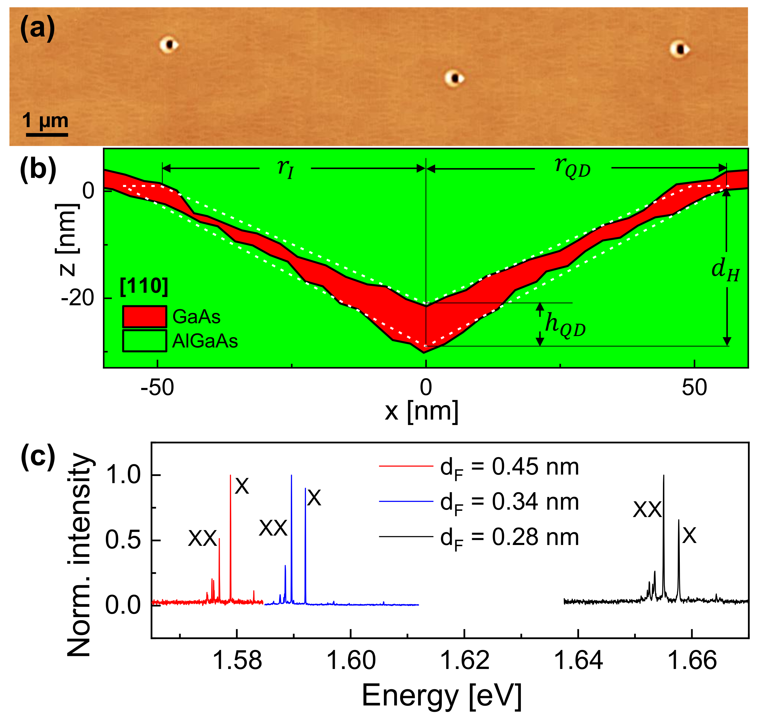
Abstract
:1. Introduction
2. QD Fabrication and Shape
3. Simulation Model
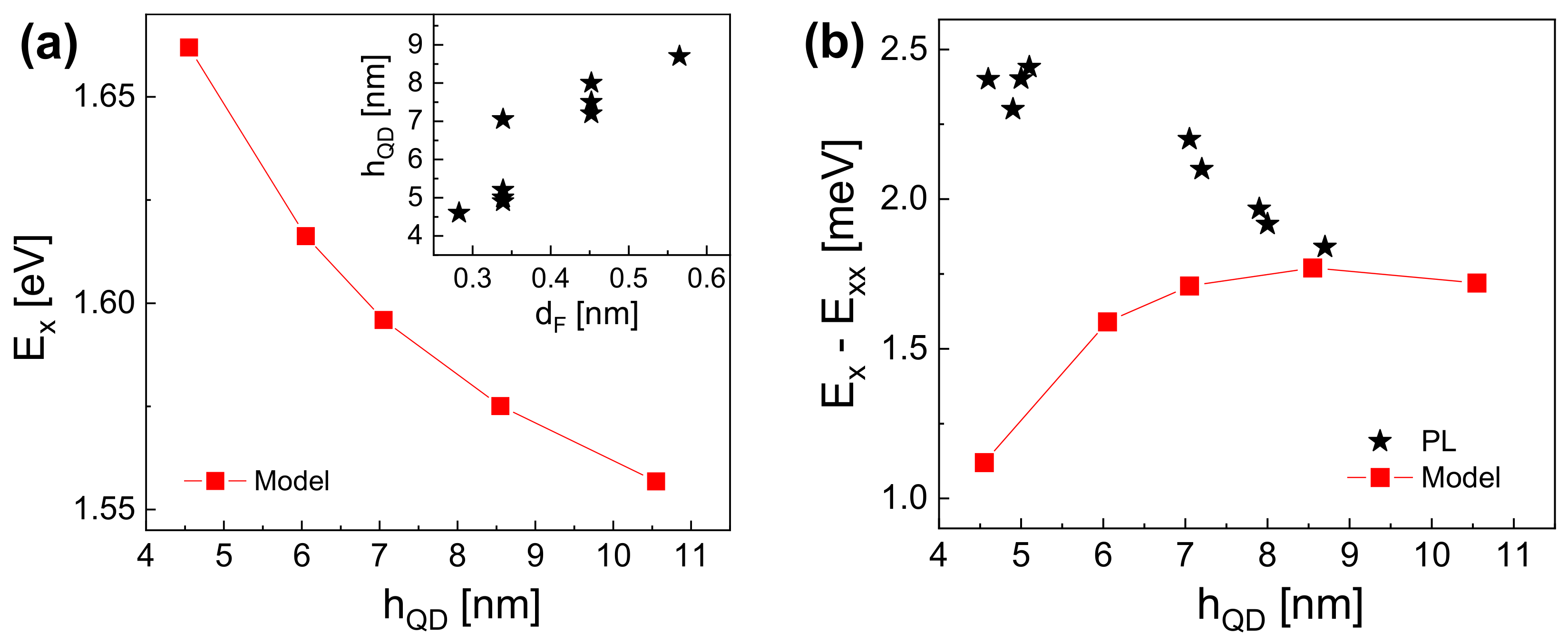
4. QD-Size Dependent Exciton Energies
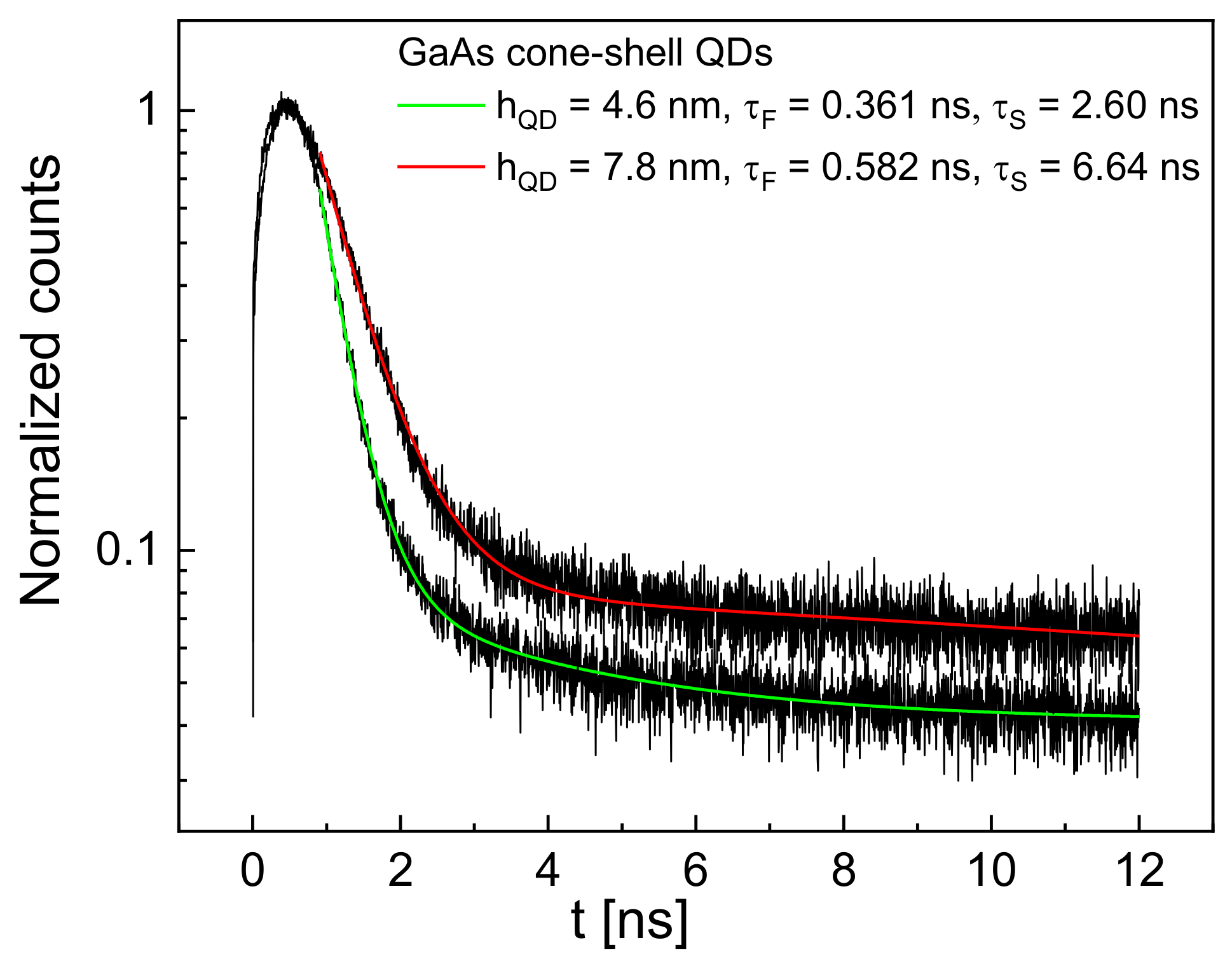
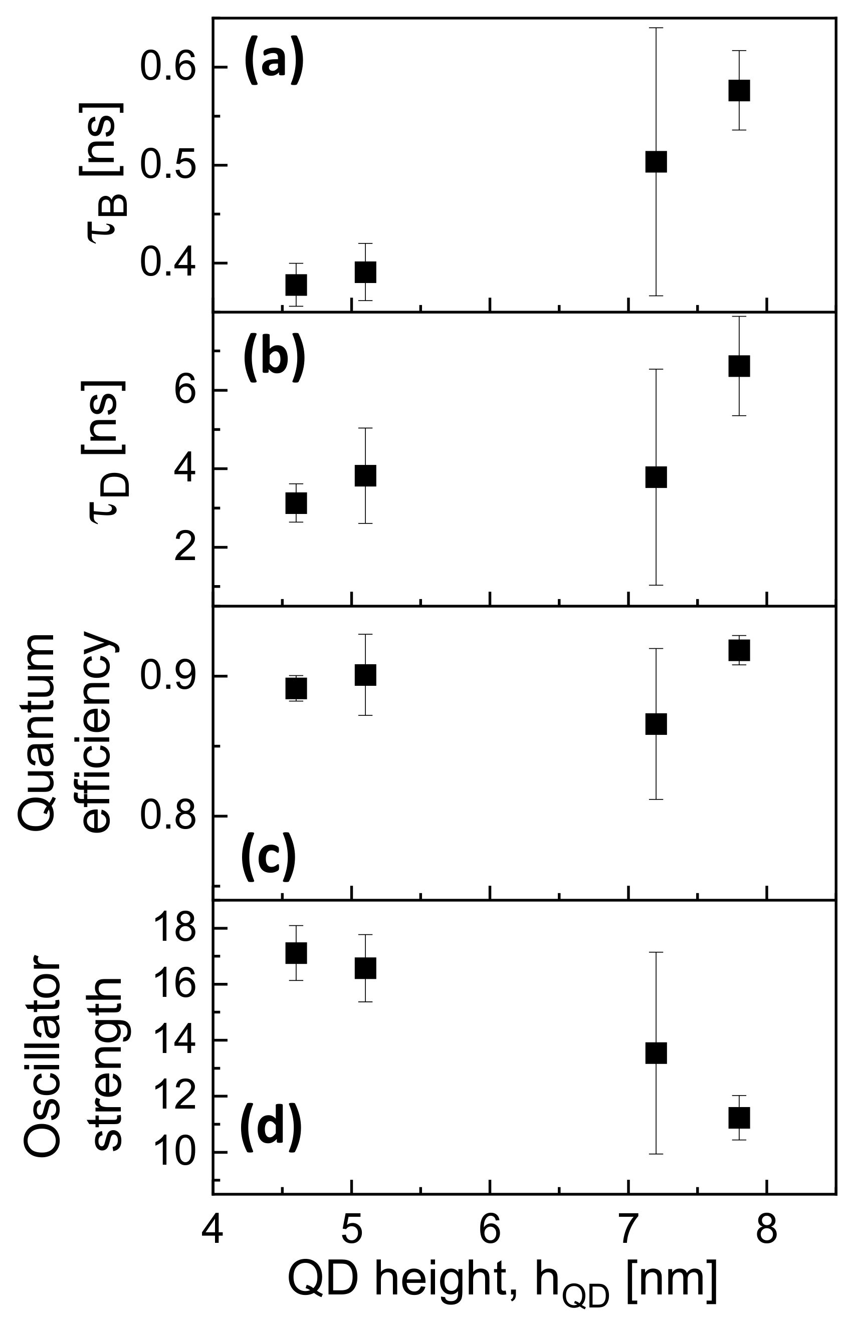
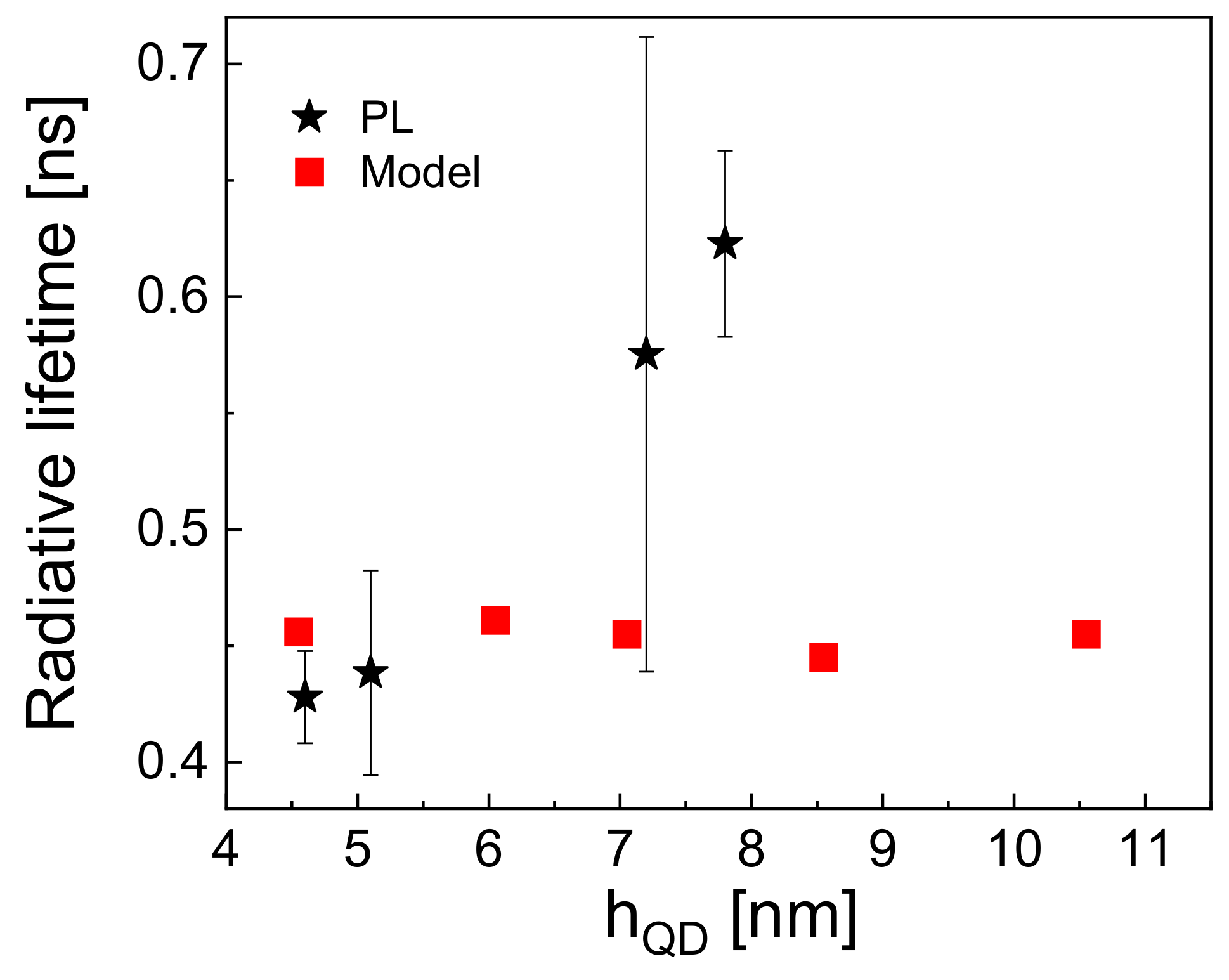
5. QD Lifetimes
6. Conclusions
Author Contributions
Funding
Institutional Review Board Statement
Informed Consent Statement
Data Availability Statement
Acknowledgments
Conflicts of Interest
References
- Somaschi, N.; Giesz, V.; Santis, L.D.; Loredo, J.C.; Almeida, M.P.; Hornecker, G.; Portalupi, S.L.; Grange, T.; Antón, C.; Demory, J.; et al. Near-optimal single-photon sources in the solid state. Nat. Photonics 2016, 10, 340–345. [Google Scholar] [CrossRef]
- Keil, R.; Zopf, M.; Chen, Y.; Höfer, B.; Zhang, J.; Ding, F.; Schmidt, O.G. Solid-state ensemble of highly entangled photon sources at rubidium atomic transitions. Nat. Commun. 2017, 8, ncomms15501. [Google Scholar] [CrossRef] [PubMed]
- Huber, D.; Reindl, M.; Huo, Y.; Huang, H.; Wildmann, J.S.; Schmidt, O.G.; Rastelli, A.; Trotta, R. Highly indistinguishable and strongly entangled photons from symmetric GaAs quantum dots. Nat. Commun. 2017, 8, ncomms15506. [Google Scholar] [CrossRef] [PubMed]
- Arakawa, Y.; Holmes, M.J. Progress in quantum-dot single photon sources for quantum information technologies: A broad spectrum overview. Appl. Phys. Rev. 2020, 7, 021309. [Google Scholar] [CrossRef]
- Lodahl, P.; Ludwig, A.; Warburton, R.J. A deterministic source of single photons. Phys. Today 2022, 75, 44–50. [Google Scholar] [CrossRef]
- Vasconcellos, S.M.D.; Gordon, S.; Bichler, M.; Meier, T.; Zrenner, A. Coherent control of a single exciton qubit by optoelectronic manipulation. Nat. Photonics 2010, 4, 545–548. [Google Scholar] [CrossRef]
- Leonard, D.; Krishnamurthy, M.; Fafard, S.; Merz, J.L.; Petroff, P.M. Molecular-beam epitaxy growth of quantum dots from strained coherent uniform islands of InGaAs on GaAs. J. Vac. Sci. Technol. B Microelectron. Nanometer Struct. Process. Meas. Phenom. 1994, 12, 1063–1066. [Google Scholar] [CrossRef]
- Madhukar, A.; Xie, Q.; Chen, P.; Konkar, A. Nature of strained InAs three-dimensional island formation and distribution on GaAs(100). Appl. Phys. Lett. 1994, 64, 2727–2729. [Google Scholar] [CrossRef]
- Moison, J.M.; Houzay, F.; Barthe, F.; Leprince, L.; André, E.; Vatel, O. Self-organized growth of regular nanometer-scale InAs dots on GaAs. Appl. Phys. Lett. 1994, 64, 196–198. [Google Scholar] [CrossRef]
- Gurioli, M.; Wang, Z.; Rastelli, A.; Kuroda, T.; Sanguinetti, S. Droplet epitaxy of semiconductor nanostructures for quantum photonic devices. Nat. Mater. 2019, 18, 799–810. [Google Scholar] [CrossRef]
- Koguchi, N.; Takahashi, S.; Chikyow, T. New MBE growth method for InSb quantum well boxes. J. Cryst. Growth 1991, 111, 688–692. [Google Scholar] [CrossRef]
- Mano, T.; Watanabe, K.; Tsukamoto, S.; Koguchi, N.; Fujioka, H.; Oshima, M.; Lee, C.D.; Leem, J.Y.; Lee, H.J.; Noh, S.K. Nanoscale InGaAs concave disks fabricated by heterogeneous droplet epitaxy. Appl. Phys. Lett. 2000, 76, 3543–3545. [Google Scholar] [CrossRef]
- Stock, E.; Warming, T.; Ostapenko, I.; Rodt, S.; Schliwa, A.; Töfflinger, J.A.; Lochmann, A.; Toropov, A.I.; Moshchenko, S.A.; Dmitriev, D.V.; et al. Single-photon emission from InGaAs quantum dots grown on (111) GaAs. Appl. Phys. Lett. 2010, 96, 093112–093114. [Google Scholar] [CrossRef]
- Wang, Z.M.; Liang, B.L.; Sablon, K.A.; Salamo, G.J. Nanoholes fabricated by self-assembled gallium nanodrill on GaAs(100). Appl. Phys. Lett. 2007, 90, 113120–113122. [Google Scholar] [CrossRef]
- Stemmann, A.; Heyn, C.; Köppen, T.; Kipp, T.; Hansen, W. Local droplet etching of nanoholes and rings on GaAs and AlGaAs surfaces. Appl. Phys. Lett. 2008, 93, 123108–123110. [Google Scholar] [CrossRef]
- Heyn, C.; Bartsch, T.; Sanguinetti, S.; Jesson, D.; Hansen, W. Dynamics of mass transport during nanohole drilling by local droplet etching. Nanoscale Res. Lett. 2015, 10, 67. [Google Scholar] [CrossRef]
- Heyn, C.; Stemmann, A.; Köppen, T.; Strelow, C.; Kipp, T.; Grave, M.; Mendach, S.; Hansen, W. Highly uniform and strain-free GaAs quantum dots fabricated by filling of self-assembled nanoholes. Appl. Phys. Lett. 2009, 94, 183113–183115. [Google Scholar] [CrossRef]
- Alonso-González, P.; Fuster, D.; González, L.; Martín-Sánchez, J.; González, Y. Low density InAs quantum dots with control in energy emission and top surface location. Appl. Phys. Lett. 2008, 93, 183106. [Google Scholar] [CrossRef]
- Heyn, C.; Klingbeil, M.; Strelow, C.; Stemmann, A.; Mendach, S.; Hansen, W. Single-dot Spectroscopy of GaAs Quantum Dots Fabricated by Filling of Self-assembled Nanoholes. Nanoscale Res. Lett. 2010, 5, 1633. [Google Scholar] [CrossRef]
- Küster, A.; Heyn, C.; Ungeheuer, A.; Juska, G.; Tommaso Moroni, S.; Pelucchi, E.; Hansen, W. Droplet etching of deep nanoholes for filling with self-aligned complex quantum structures. Nanoscale Res. Lett. 2016, 11, 282. [Google Scholar] [CrossRef] [Green Version]
- Vonk, V.; Slobodskyy, T.; Keller, T.F.; Richard, M.I.; Fernández, S.; Schulli, T.; Heyn, C.; Hansen, W.; Stierle, A. Faceting of local droplet-etched nanoholes in AlGaAs. Phys. Rev. Mater. 2018, 2, 106001. [Google Scholar] [CrossRef]
- Heyn, C.; Küster, A.; Zocher, M.; Hansen, W. Field-Controlled Quantum Dot to Ring Transformation in Wave-Function Tunable Cone-Shell Quantum Structures. Phys. Status Solidi (RRL) – Rapid Res. Lett. 2019, 13, 1800245. [Google Scholar] [CrossRef]
- Keating, P.N. Effect of Invariance Requirements on the Elastic Strain Energy of Crystals with Application to the Diamond Structure. Phys. Rev. 1966, 145, 637. [Google Scholar] [CrossRef]
- Williamson, A.J.; Wang, L.W.; Zunger, A. Theoretical interpretation of the experimental electronic structure of lens-shaped self-assembled InAs/GaAs quantum dots. Phys. Rev. B 2000, 62, 12963. [Google Scholar] [CrossRef]
- Luo, J.W.; Bester, G.; Zunger, A. Atomistic pseudopotential theory of droplet epitaxial GaAs/AlGaAs quantum dots. In Nanodroplets; Wang, Z.M., Ed.; Springer: New York, NY, USA, 2013; pp. 329–361. [Google Scholar] [CrossRef]
- Bester, G. Electronic excitations in nanostructures: An empirical pseudopotential based approach. J. Phys. Condens. Matter 2009, 21, 023202. [Google Scholar] [CrossRef]
- Wang, L.W.; Zunger, A. Linear combination of bulk bands method for large-scale electronic structure calculations on strained nanostructures. Phys. Rev. B 1999, 59, 15806. [Google Scholar] [CrossRef]
- Foresman, J.B.; Head-Gordon, M.; Pople, J.A.; Frisch, M.J. Toward a systematic molecular orbital theory for excited states. J. Phys. Chem. 1992, 96, 135–149. [Google Scholar] [CrossRef]
- Franceschetti, A.; Fu, H.; Wang, L.W.; Zunger, A. Many-body pseudopotential theory of excitons in InP and CdSe quantum dots. Phys. Rev. B 1999, 60, 1819. [Google Scholar] [CrossRef]
- Bester, G.; Nair, S.; Zunger, A. Pseudopotential calculation of the excitonic fine structure of million-atom self-assembled InGaAs/GaAs quantum dots. Phys. Rev. B 2003, 67, 161306. [Google Scholar] [CrossRef]
- Resta, R. Thomas-Fermi dielectric screening in semiconductors. Phys. Rev. B 1977, 16, 2717–2722. [Google Scholar] [CrossRef]
- Graf, A.; Sonnenberg, D.; Paulava, V.; Schliwa, A.; Heyn, C.; Hansen, W. Excitonic states in GaAs quantum dots fabricated by local droplet etching. Phys. Rev. B 2014, 89, 115314. [Google Scholar] [CrossRef]
- Tighineanu, P.; Daveau, R.; Lee, E.H.; Song, J.D.; Stobbe, S.; Lodahl, P. Decay dynamics and exciton localization in large GaAs quantum dots grown by droplet epitaxy. Phys. Rev. B 2013, 88, 155320. [Google Scholar] [CrossRef]
- Narvaez, G.A.; Bester, G.; Franceschetti, A.; Zunger, A. Excitonic exchange effects on the radiative decay time of monoexcitons and biexcitons in quantum dots. Phys. Rev. B 2006, 74, 205422. [Google Scholar] [CrossRef] [Green Version]


Publisher’s Note: MDPI stays neutral with regard to jurisdictional claims in published maps and institutional affiliations. |
© 2022 by the authors. Licensee MDPI, Basel, Switzerland. This article is an open access article distributed under the terms and conditions of the Creative Commons Attribution (CC BY) license (https://creativecommons.org/licenses/by/4.0/).
Share and Cite
Heyn, C.; Gräfenstein, A.; Pirard, G.; Ranasinghe, L.; Deneke, K.; Alshaikh, A.; Bester, G.; Hansen, W. Dot-Size Dependent Excitons in Droplet-Etched Cone-Shell GaAs Quantum Dots. Nanomaterials 2022, 12, 2981. https://doi.org/10.3390/nano12172981
Heyn C, Gräfenstein A, Pirard G, Ranasinghe L, Deneke K, Alshaikh A, Bester G, Hansen W. Dot-Size Dependent Excitons in Droplet-Etched Cone-Shell GaAs Quantum Dots. Nanomaterials. 2022; 12(17):2981. https://doi.org/10.3390/nano12172981
Chicago/Turabian StyleHeyn, Christian, Andreas Gräfenstein, Geoffrey Pirard, Leonardo Ranasinghe, Kristian Deneke, Ahmed Alshaikh, Gabriel Bester, and Wolfgang Hansen. 2022. "Dot-Size Dependent Excitons in Droplet-Etched Cone-Shell GaAs Quantum Dots" Nanomaterials 12, no. 17: 2981. https://doi.org/10.3390/nano12172981
APA StyleHeyn, C., Gräfenstein, A., Pirard, G., Ranasinghe, L., Deneke, K., Alshaikh, A., Bester, G., & Hansen, W. (2022). Dot-Size Dependent Excitons in Droplet-Etched Cone-Shell GaAs Quantum Dots. Nanomaterials, 12(17), 2981. https://doi.org/10.3390/nano12172981