Article

Insight into the Effect of Selenization Temperature for Highly Efficient Ni-Doped Cu2ZnSn(S,Se)4 Solar Cells

1
Key Laboratory of Functional Materials Physics and Chemistry of the Ministry of Education, Jilin Normal University, Siping 136000, China
2
State Key Laboratory of Superhard Materials, College of Physics, Jilin University, Changchun 130012, China
*
Author to whom correspondence should be addressed.
Nanomaterials 2022, 12(17), 2942; https://doi.org/10.3390/nano12172942
Submission received: 7 August 2022 / Revised: 22 August 2022 / Accepted: 22 August 2022 / Published: 26 August 2022
(This article belongs to the Special Issue Solar Thin Film Nanomaterials and Nanodevices)

Abstract

:
Cu2Ni0·05Zn0·95Sn(S,Se)4 (CNZTSSe) films were synthesized on Mo-coated glass substrates by the simple sol–gel means combined with the selenization process, and CNZTSSe-based solar cells were successfully prepared. The effects of selenization temperature on the performance and the photoelectric conversion efficiency (PCE) of the solar cells were systematically studied. The results show that the crystallinity of films increases as the selenization temperature raises based on nickel (Ni) doping. When the selenization temperature reached 540 °C, CNZTSSe films with a large grain size and a smooth surface can be obtained. The Se doping level gradually increased, and Se occupied the S position in the lattice as the selenization temperature was increased so that the optical band gap (Eg) of the CNZTSSe film could be adjusted in the range of 1.14 to 1.06 eV. In addition, the Ni doping can inhibit the deep level defect of SnZn and the defect cluster [2CuZn + SnZn]. It reduces the carrier recombination path. Finally, at the optimal selenization temperature of 540 °C, the open circuit voltage (Voc) of the prepared device reached 344 mV and the PCE reached 5.16%.

1. Introduction

In recent years, Cu2ZnSn(S,Se)4 (CZTSSe) thin films have become a new photovoltaic material. CZTSSe films have p-type conductivity, an ideal optical absorption coefficient of about 104 cm−1, and an Eg of 1.0–1.5 eV [1,2,3,4,5,6]. At present, through people’s continuous efforts, the PCE of Cu2ZnSnS4 (CZTS) solar cells reached a record 12.6% from 0.66% in 2014 years [7]. However, it is still far from the theoretical efficiency. The theoretical PCE of CZTS-based solar cells is up to 32.2% [8,9]. The efficiency of CZTSSe devices has not been further improved at the moment. The key factors are the low Voc and high open voltage loss.
Recent studies have shown that the rich inherent defects in thin-film solar cells will lead to a short minority carrier life and harmful band gap potential fluctuations, thus increasing the loss of open circuit voltage [10,11,12]. To improve this low Voc, it is an effective strategy to add isovalent cations into kesterite CZTSSe to replace Cu, Zn, or Sn and decrease harmful inherent defects [13,14,15,16]. In our previous work, we selected Ni ions with the closest radius to Zn ions for equivalent substitution doping, which effectively suppressed the intrinsic defects in the crystal: CuZn anti-site defects and (2Cuzn + SnZn) defect clusters. The experimental results show that the Voc value of CNZTSSe devices with the optimal Ni doping content is 42 mV higher than that of CZTSSe devices. In the process of preparing CNZTSSe devices, the CNZTSSe absorption layer is usually synthesized by a two-step process. First, a CNZTS precursor film with an appropriate element composition is deposited. Then, the precursor films are heat treated in a selenium-rich environment. Consequently, to further obtain high-quality CNZTSSe devices, it is necessary to optimize the selenization conditions of CNZTSSe films [17,18,19].
At present, the influence of the post-annealing temperature on the performances of the films has been reported in many works. For example, Kamoun et al. deposited CZTS by adjusting the post-annealing temperature [20]. They found that the post-annealing temperature is vital to enhance the properties of thin films. The IBM group deposited an undoped CZTSSe absorber through post-annealing treatment at 375 °C to improve equipment efficiency [21]. The results indicate that the post-annealing treatment can effectively enhance the crystal quality of the films [20,21]. So far, the effects of selenization temperature on the performances of CNZTSSe films and solar cells have not been studied and reported in detail.
In this work, we successfully deposited CNZTS precursor films on the Mo-coated glass substrates and the CNZTS precursor films were then post-annealed in a selenization atmosphere. By adjusting the selenization temperature, we systematically explored the influence of selenization temperature on the grain growth, photoelectric performances of CNZTSSe films, and CNZTSSe device efficiency. Our work shows that the selenization temperature has an obvious effect on the crystallinity of the films. The film surface is smooth, compact, and almost without holes at the optimum selenization temperature (540 °C), which can effectively reduce grain boundaries, avoid the recombination of minority carriers at grain boundaries, and improve the carrier concentration. Finally, we successfully prepared CNZTSSe solar cells with a PCE of 5.16% by optimizing the selenization temperature.

2. Experimental

2.1. Preparation of CNZTSSe Thin Films

Using dimethyl Acer (DMSO) (Aladdin, Shanghai Aladdin Biochemical Technology Co., Ltd., Shanghai, China, 99.99%) as the solvent, C4H6CuO4·H2O (Aladdin, Shanghai Aladdin Biochemical Technology Co., Ltd., Shanghai, China, 99.99%), ZnCl2 (Aladdin, Shanghai Aladdin Biochemical Technology Co., Ltd., Shanghai, China, 99.99%), NiNO3·6H2O (Sinopharm Chemical Reagent Co., Ltd. Shanghai, China 99.99%), SnCl2·2H2O (Aladdin, Shanghai Aladdin Biochemical Technology Co., Ltd., Shanghai, China, 99.99%), and CH4N2S (Aladdin, Shanghai Aladdin Biochemical Technology Co., Ltd., Shanghai, China, 99.99%) as solutes, the CNZTS precursor solution was obtained by overall dissolution, stirring, and heating for 1 h. Then, the above solution was deposited on the Mo-coated sodium calcium glass (SLG) substrate with a rotating speed of 3000 rpm and a spin coating time of 30 s and then dried on a hot plate with a temperature of 300 °C in a nitrogen atmosphere. This step was repeated 10 times to obtain a film thickness of 1 um as required by our experiment. Finally, the films were annealed at a high temperature in a selenium-rich environment with 130 mg selenium particles (Aladdin, Shanghai Aladdin Biochemical Technology Co., Ltd., Shanghai, China, 99.99%) as the selenium source. The annealing time was 15 min and the annealing temperatures were set to 500, 520, 540, and 560 °C for different samples. The synthesis of CNZTSSe films was finished via natural cooling to room temperature.

2.2. Preparation of CNZTSSe Devices

The structure of CNZTSSe solar cells is an SLG/Mo/CNZTSSe/CdS/i-ZnO/ITO/Ag grid. A CdS buffer layer was synthesized on the CNZTSSe layer using chemical bath deposition (CBD), and then ZnO and ITO layers were continuously deposited onto the CdS buffer layer using magnetron sputtering. A thin film silver electrode (~900 nm) was prepared on the ITO layer via thermal evaporation means, and nine devices with an effective area of 0.19 cm2 were prepared via mechanical scribing.

2.3. Characterization

The structural characteristics of the films were evaluated via X-ray diffraction (XRD) (Rigaku Corporation, Tokyo, Japan) using Cu Ka (λ = 0.15406 nm). A Renishaw system instrument using an excitation wavelength of 514 nm was run to record the Raman spectrum and test the phase purity. Scanning electron microscopy (SEM) (Hitachi, S-4800, JEOL, Tokyo, Japan) was used to observe the surface morphology of the films. The chemical composition of CNZTSSe films was measured via X-ray photoelectron spectroscopy (XPS) (Thermofisher, Waltham, MA, USA). The constituent element contents of CNZTSSe films were determined by energy-dispersive X-ray spectroscopy (EDS) (Hitachi, S-4800, JEOL, Tokyo, Japan). The electrical and optical performances of CNZTSSe films were investigated by the use of a Hall effect measurement system and an ultraviolet-visible-near-infrared spectrophotometer (UV-3101PC, Tokyo, Japan), respectively. External quantum efficiency (EQE) curves were measured by a Zolix solar cell Scan100 measuring instrument (Zolix, Beijing Zhuoli Hanguang Instrument Co., Ltd., Beijing, China). For the PCE measurement of CNZTSSe-based devices, the current density–voltage (J-V) plots were obtained with a Model 91160 Oriel semiconductor parametric analyzer (Model 94043A, Oriel, Australia) under the simulated AM 1.5 total solar radiation (100 mW/cm2).

3. Results and Discussion

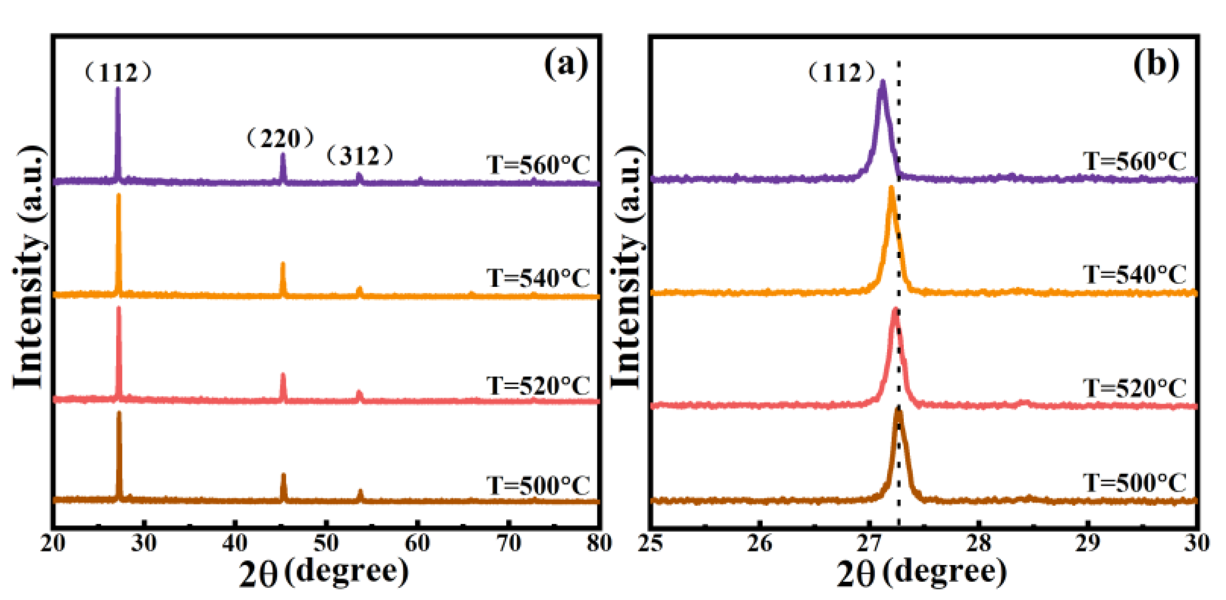
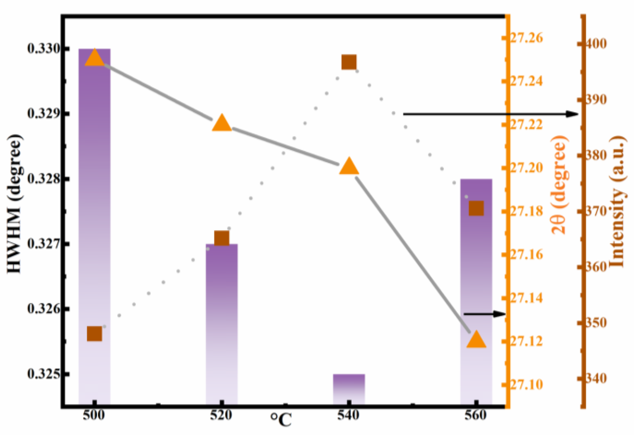
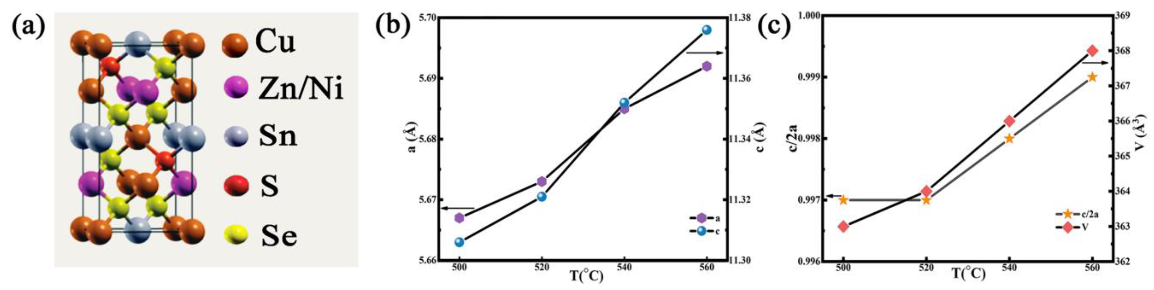
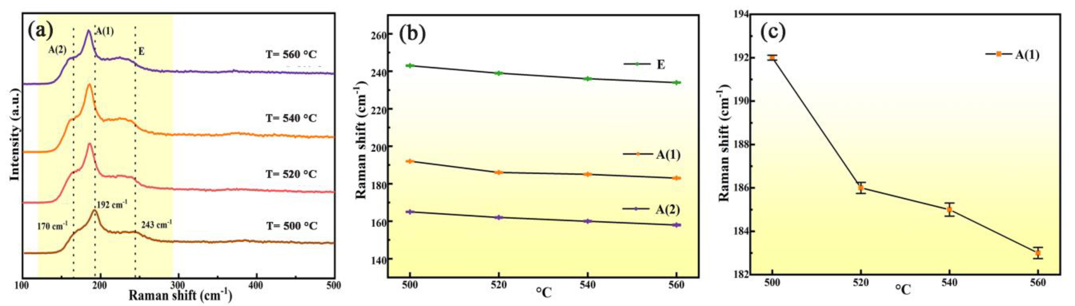
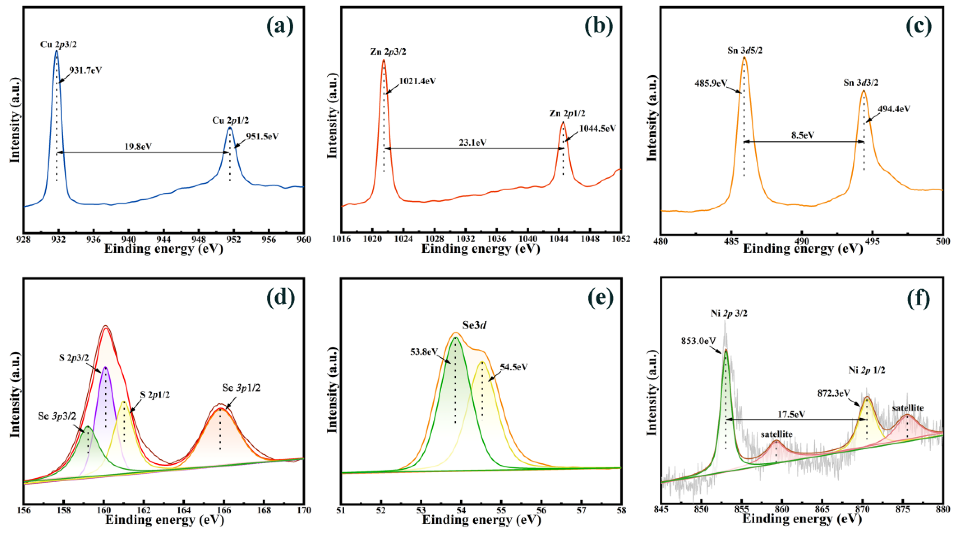
3.1. Structure and Morphology of Thin Films

Figure 1 displays the preparation process of the CNZTSSe films. First, a CNZTS film was deposited on SLG using the spin coating method, and then the CNZTSSe films were obtained by selenization annealing. To promote the grain growth of the film during selenization annealing, the selenization temperatures were set to 500, 520, 540, and 560 °C. To reveal the effect of selenization temperature on the crystal structure of the CNZTSSe film, the XRD patterns (Figure 2a) were recorded for the film prepared at various selenization temperatures. There are three main peaks near 2θ = 27.34°, 45.51°, and 53.63° for all films, corresponding to the (112), (220), and (312) crystal planes of CZTSSe, respectively [22,23]. At the same time, no foreign peaks were observed, which means that the selenization temperature has a little effect on the film structure and is not changing the crystal structure of the film. The enlarged (112) peaks are presented in Figure 2b. The change trend can be summarized as follows: with selenization temperature raising, the diffraction angle shifts from 27.25° to 27.12°. This clearly reveals that Se replaces S in the lattice, and this peak position change is owed to the change in unit cell volume caused via the larger Se replacing S in the lattice.
To analyze the function of selenization temperature on the grain growth, the curves of 2θ, peak intensity, and half peak width (FWHM) with respect to selenization temperature were drawn by using the test data of XRD. Along with the selenization temperature increasing, the value of 2θ gradually decreased, as shown in Figure 3. Meanwhile, the peak intensity gradually strengthens and the corresponding FWHM decreases. At the optimal selenization temperature (540 °C), the peak intensity is the strongest and the FWHM value is minimal. The results show that the film crystallinity is significantly enhanced. The film crystallinity is very important to obtain ideal thin films. Therefore, it is meaningful to adjust the selenization temperature for obtaining high-quality devices.
The lattice constants a and c, unit cell volume (V), and lattice parameters (η = c/2a) were calculated on the basis of the XRD pattern, as shown in Figure 4b,c. Figure 4a shows a kesterite structure of CNZTSSe. As the selenization temperature is increased, a and c increase, as shown in Figure 4b. Accordingly, V also increases. This is because the larger Se replaces the positions of S in the lattice and the number of Se-substituted S atoms gradually increases, which finally expands the lattice. In Figure 4c, it can be found that all η values are lower than 1. According to the study of Quaternary Chalcogenide Semiconductor structure, η values less than 1 correspond to the crystal structure of the kesterite phase [24]. Therefore, the above results prove that the crystal structure of CNZTSSe films is not changed and it is still a pure kesterite type phase [25].
Raman measurements are more accurate for analyzing the impurity phases in the films. Because the diffraction peaks of typical secondary phases and CZTSSe phases are very close, it is difficult to distinguish them only by XRD analysis [26]. Figure 5a shows the Raman spectra of all films. It was found that CNZTSSe films show almost the same Raman spectra at different selenization temperatures. All films had three vibration peaks at 170, 192, and 243 cm−1. The vibration peaks at 170 and 192 cm−1 belong to A-mode Raman vibration peaks of CZTSSe phase, and the vibration peak at 243 cm−1 belongs to E vibrational mode Raman peak of CZTSSe phase [27,28]. In addition to the above three vibration peaks, no other vibration peaks were found. This result means that there are no impurity phases in the films. The Raman test results accord well with the above XRD test results. Figure 5b displays the wavenumbers of the three vibration peaks as a function of selenization temperature. The dependence for the main A (1) mode vibration peak is given in Figure 5c. Combining Figure 5b,c, it can be found that the main Raman vibration peak of A (1) has an obvious red shift, and other vibration peaks also have similar changes. The reason for this phenomenon is that the larger Se atom was successfully incorporated into the lattice, replacing the smaller S atom, which correlates well with the XRD results.
XPS was applied to characterize the composition and the valence states of elements in the CNZTSSe film (540 °C). The representative spectrum of the Cu 2p doublet is presented in Figure 6a. There were two peaks at 931.7 and 951.5 eV, which were identified as Cu 2p3/2 and Cu 2p1/2 components, respectively. The binding energy interval is 19.80 eV, indicating that Cu+ exists in CNZTSSe [29]. Figure 6b displays the Zn 2p XPS spectrum, where the Zn 2p3/2 peak was found at 1021.4 eV and the Zn 2p1/2 peak was found at 1044.5 eV. The peak splitting value is 23.1 eV, indicating that Zn exists only in the form of a +2 valence [30]. The XPS spectra of Sn 3d (Figure 6c) indicate two characteristic peaks: Sn 3d5/2 at 485.9 eV and Sn 3d3/2 at 494.4 eV. The splitting value is 8.5 eV, which refers to Sn4+ [31]. The XPS spectrum of S 2p is presented in Figure 6d [32,33,34]. The S 2p and Se 3p peak positions are very close. Therefore, the XPS spectrum in Figure 6d shows four characteristic peaks by Gaussian fitting. The characteristic peaks at 159.20, 160.08, 161.02, and 165.84 eV could belong to Se 3p3/2, S 2p3/2, S 2p1/2, and Se 3p1/2, respectively. The peaks at 160.08 eV and 161.02 eV are in accordance with the 160–164 eV range of S2− [35]. As displayed in the Se 3d XPS spectrum (Figure 6e), the peaks at 53.8 and 54.5 eV are attributed to the characteristic peaks of Se 3d3/2 and Se 3d1/2 for the Se2− oxidation state [36,37,38]. Figure 6f shows that the peaks at 853.0 and 872.3 eV are correspondent to Ni 2p3/2 and Ni 2p1/2 components. The binding energy difference between the Ni 2p components is 17.5 eV, and it is in good relation with the splitting value of Ni2+ [39,40]. The above experimental results show that the constituent elements of the film exist in the valence states of Cu+, Ni2+, Zn2+, Sn4+, S2−, and Se2−.
The content of the elements in the film was obtained by EDS test, and its content was analyzed according to the test results. Table 1 summarizes the EDS test data of CNZTSSe films selenized at 500, 520, 540, and 560 °C. It can be found that, except for Se and S elements, the contents of other elements and the element content ratio related to Ni have almost no significant changes. It should be noted that the fluctuation in Ni content in the film is very small with the selenization temperature rising, which means that there is no loss of Ni content in the selenization process. This helps to inhibit the formation of Zn-related defects, such as CuZn and SnZn anti-site defects. In addition, EDS test results indicate that Se content increases by 4% and S content decreases by 2.4% with the selenization temperature rising. This reveals that CNZTSSe films were synthesized under the condition of Se enrichment. At the same time, it also shows that the substitution of the Se atom for the S atom is enhanced. This further supports the conclusion obtained from the XRD results that the Se atom successfully replaces the position of S in the lattice.
Figure 7a–d show the SEM images of the top surfaces of the CNZTSSe films selenized at 500, 520, 540, and 560 °C. It can be seen in Figure 7a that when the selenization temperature is 500 °C, the grains are at the initial stage of growth, and they are small. When the selenization temperature rises to 520 °C, the grains grow further, and the grain size becomes larger. However, the small grain layer still exists, and the film’s surface is rough with many voids (Figure 7b). When the selenization temperature is 540 °C, it is obvious that small grains and holes are eliminated. Meanwhile, the grain size reaches micron level, and the morphology of the CNZTSSe film is smooth and dense, as shown in Figure 7c. When the selenization temperature further rose to 560 °C, although the grain size was large, voids began to appear in Figure 7d. The above results show that selenization temperature can promote the grain growth and reduce grain boundaries, which is beneficial to suppress the carrier non-radiative recombination at the grain boundaries [21]. In addition, it is obviously observed that the optimal selenization temperature is 540 °C.

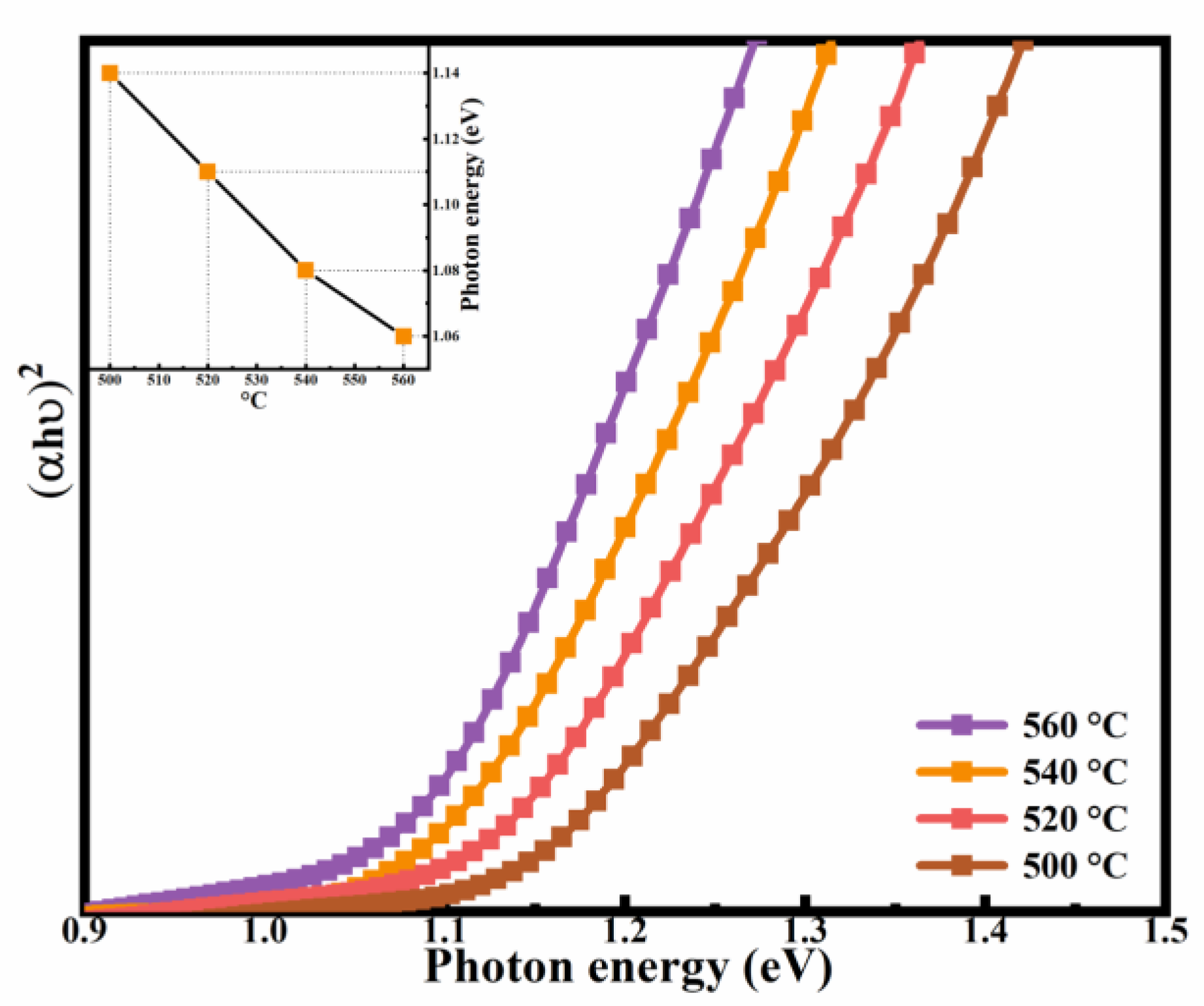
3.2. Optical and Electrical Performances of Thin Films

To determine the influence of selenization temperature on the Eg values in the films, UV-vis-NIR spectra measurements were carried out. The absorption spectra of all samples were obtained, and Figure 8 shows the (αhυ)2-hυ curves of the CNZTSSe films. The Eg values can be estimated by processing the optical absorption spectra with the use of the Tauc relation:
(αhυ) = B (hυ − Eg) n
where α is the absorption coefficient, hυ is the Photon energy, and B is a constant [41,42,43,44]. Theoretical studies show that n corresponds to 1/2, 3/2, 2, and 3 in permitted direct transition, permitted indirect transition, prohibited direct transition, and prohibited indirect transition, respectively [45]. CNZTSSe films are direct bandgap semiconductors, so the value of n is 1/2. Therefore, Equation (2) can be obtained from Equation (1), as follows:
(αhυ) = B (hυ − Eg) 1/2
According to Equation (2), Eg can be gained by inferring the linear part of the curve (αhυ)2 as a function of hυ to intercept the energy x-axis. When (αhυ)2 = 0, Eg = hυ. The Eg values of the CNZTSSe absorption layers selenized at 500, 520, 540, and 560 °C are arranged in the inset of Figure 8. When the selenization temperatures are 500, 520, 540, and 560 °C, the Eg values are equal to 1.14, 1.11, 1.08, and 1.06 eV, respectively. Then, according to the curve given in the inset, it can be found that the value of Eg diminishes with the rising selenization temperature. Everyone knows that the Eg of CZTSe is smaller than that of CZTS [46]. According to the EDS test, as the selenization temperature rises, the content of Se rises and the content of S lessens. Therefore, the Eg of CNZTSSe will be closer to the small Eg of CZTSe as the Se content rises. Moreover, according to the first principal calculation, when Se replaces S, the orbital interaction between the valence band (VBM) top and the conduction band (CBM) bottom is weakened, thus reducing Eg (i.e., CBM = VBM + Eg) [47].
The electrical performances of CNZTSSe films were studied via Hall measurement at room temperature. The test was carried out several times to improve the accuracy of the results. The test results are shown in Table 2. All CNZTSSe films show p-type conductivity. This is mainly ascribed to the typical high concentration of intrinsic CuZn anti-site defects in the film, which will make the Fermi level close to VBM, so that the film has p-type conductivity [48]. During the increase in the selenization temperature, the carrier concentration increased from 2.2 × 1016 cm−3 to 1.15 × 1017 cm−3 and then reduced to 1.35 × 1016 cm−3. The corresponding Hall mobility decreased from 1.27 to 1.15 cm2V−1s−1 and then increased to 1.71 cm2V−1s−1. However, at the selenization temperature of 540 °C, the carrier concentration is the highest, which is due to the improvement in film quality, the reduction in the number of grain boundaries, and the reduction in carrier recombination at grain boundaries, thus effectively increasing the carrier concentration. However, when the carrier concentration increases, the carrier scattering will increase, resulting in a decrease in mobility.

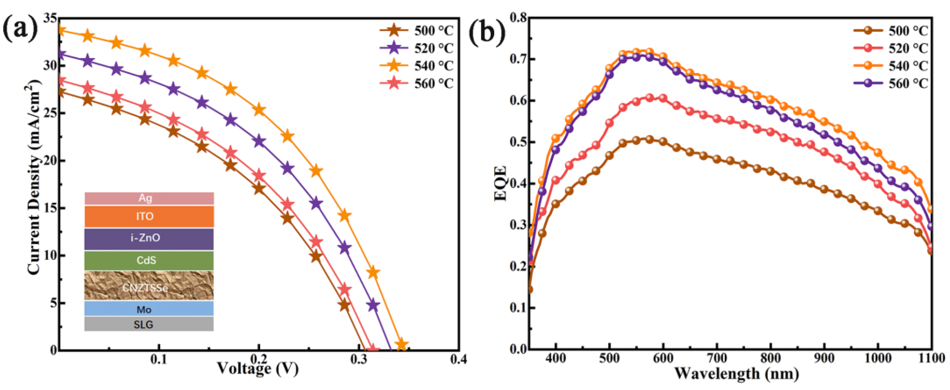
3.3. Device Performance

To reveal the impact mechanism of selenization temperature on the PCE, CNZTSSe devices with traditional structures were prepared by using CNZTSSe as an absorption layer after the selenization at 500, 520, 540, and 560 °C. The main performance parameters of the corresponding devices are listed in Table 3. Figure 9a shows the J-V curves of CNZTSSe solar cells for different selenization temperatures. The layer structure of the prepared CNZTSSe solar cells is given in Figure 9a. Comparing the data presented in Table 3, it can be found that the PCE of the device increases from 3.56 to 5.16% as the selenization temperature rises from 500 to 540 °C, and when the temperature is further increased to 560 °C, the PCE level of the device decreases to 3.68%. Meanwhile, the series resistance (Rs) of the device gradually decreases until it reaches the minimum value at 540 °C. However, the corresponding shunt resistance (Rsh) rises with the rising selenization temperature and the selenization temperature corresponding to the maximum value is 540 °C. The decrease in Rs can be attributed to the enhancement of film crystallinity and the decrease of crystal boundaries, which reduces the recombination rate of carriers at the grain boundaries. The increase in Rsh is due to the smooth and dense CNZTSSe film providing a good substrate for the deposition of the CdS layer so that CdS can be deposited evenly on the surface of the CNZTSSe film and reduce the recombination of carriers at the interface. The Rs lessens and Rsh increases, leading to the increase in the short circuit current density (Jsc) and filling factor (FF), which finally leads to the increase in Voc. The variation curves of the above main parameters are shown in Figure 10. To sum up, we find that the champion PCE is 5.16% for the device with Voc of 344 mV, Jsc of 33.63 mA/cm2, and FF of 44.56% when the selenization temperature is 540 °C.
Figure 9b displays the EQE levels of CNZTSSe devices for different selenization temperatures. The results show that the EQE of the device increases significantly in the whole wavelength range from 350 to 1100 nm when the selenization temperature rises from 500 to 540 °C. The improvement of EQE is mainly due to the optimization of the crystal quality of the film, allowing more photons to be absorbed [49]. In addition, the improvement in the EQE shows that the carrier recombination is reduced and the charge collection in the space charge region is enhanced [50]. Yet, when the selenization temperature further rose to 560 °C, the EQE spectral response decreased. This may be caused by the following two aspects. For one thing, the decomposition of the CNZTSSe phase may occur at higher selenization temperatures. For another, due to the film roughness increase at higher selenization temperatures, the formation of a poor PN junction may occur [51]. The above results show that the EQE response of the structure is the most significant at the optimal selenization temperature (540 °C).

4. Conclusions

In summary, the single-phase kesterite CNZTSSe thin films were obtained by the simple sol–gel method and selenization process in the temperature range of 500–560 °C. The results show that PCE can be increased from 3.56 to 5.16% by regulating the selenization temperature of CNZTSSe films. The increase in PCE is mainly owed to the increase in Voc, which derives from the decrease in Eg and the increase in FF and Jsc. The PCE changes with the selenization temperature and the PCE can be up to a maximum value of 5.16% for solar cells synthesized using the CNZTSSe absorption layer film selenized at 540 °C. It is proven that the enhancement of PCE with selenization temperature is mainly attributed to the decrease in Rs and the increase in Rsh. The improvement in Rs and Rsh depends on the enhancement of the crystal quality and grain size of the CNZTSSe film. In addition, Ni doping in CZTSSe films can alleviate the negative effects of defects from SnZn and [2CuZn + SnZn] on devices at 540 °C, which reduces the carrier recombination rate and increases the carrier concentration.

Author Contributions

Conceptualization, Y.S. and F.Z.; Writing-Original Draft Preparation, F.Z.; Software, M.M., N.Z. and T.W.; Formal analysis, Y.S. and Z.W.; Investigation, Y.S. and F.W.; Writing-Review & Editing, L.Y., H.L. and B.Y. All authors have read and agreed to the published version of the manuscript.

Funding

This research was funded by the Program for the development of Science and Technology of Jilin province Grant Nos. 20210101410JC, 20210509050RQ.

Institutional Review Board Statement

Not applicable.

Informed Consent Statement

Informed consent was obtained from all subjects involved in the study.

Conflicts of Interest

The authors declare no conflict of interest.

References

  1. Yu, Q.; Shi, J.J.; Guo, L.B.; Duan, B.W.; Luo, Y.H.; Wu, H.J.; Li, D.M.; Meng, Q.B. Eliminating multi-layer crystallization of Cu2ZnSn(S,Se)4 absorber by controlling back interface reaction. Nano Energy 2020, 76, 105042. [Google Scholar] [CrossRef]
  2. Su, Z.H.; Liang, G.X.; Fan, P.; Luo, J.T.; Zheng, Z.H.; Xie, Z.G.; Wang, W.; Chen, S.; Hu, J.G.; Wei, Y.D.; et al. Device Postannealing Enabling over 12% Efficient Solution-Processed Cu2ZnSn(S,Se)4 Solar Cells with Cd(2+) Substitution. Adv. Mater. 2020, 32, 12. [Google Scholar] [CrossRef] [PubMed]
  3. Yang, K.J.; Son, D.H.; Sung, S.J.; Sim, J.H.; Kim, Y.I.; Park, S.N.; Jeon, D.H.; Kim, J.; Hwang, D.K.; Jeon, C.W.; et al. A band-gap-graded CZTSSe solar cell with 12.3% efficiency. J. Mater. Chem. A 2016, 4, 10151–10158. [Google Scholar] [CrossRef]
  4. Tiwari, D.; Koehler, T.; Lin, X.; Harniman, R.; Griffiths, I.; Wang, L.; Cherns, D.; Klenk, R.; Fermin, D.J. Cu2ZnSnS4 Thin Films Generated from a Single Solution Based Precursor: The Effect of Na and Sb Doping. Chem. Mater. 2016, 28, 4991–4997. [Google Scholar] [CrossRef]
  5. Sengar, B.S.; Garg, V.; Kumar, A.; Awasthi, V.; Kumar, S.; Atuchin, V.V.; Mukherjee, S. Band alignment of Cd-free (Zn,Mg)O layer with Cu2 ZnSn(S,Se)4 and its effect on the photovoltaic properties. Opt. Mater. 2018, 84, 748–756. [Google Scholar] [CrossRef]
  6. Sengar, B.S.; Garg, V.; Siddharth, G.; Kumar, A.; Pandey, S.K.; Dubey, M.; Atuchin, V.V.; Kumar, S.; Mukherjee, S. Improving the Cu2ZnSn(S,Se)4—Based Photovoltaic Conversion Efficiency by Back-Contact Modification. IEEE Trans. Electron. Devices 2021, 68, 2748–2752. [Google Scholar] [CrossRef]
  7. Williams, B.A.; Smeaton, M.A.; Trejo, N.D.; Francis, L.F.; Aydil, E.S. Effect of Nanocrystal Size and Carbon on Grain Growth during Annealing of Copper Zinc Tin Sulfide Nanocrystal Coatings. Chem. Mater. 2017, 29, 1676–1683. [Google Scholar] [CrossRef]
  8. Ki, W.; Hillhouse, H.W. Earth-Abundant Element Photovoltaics Directly from Soluble Precursors with High Yield Using a Non-Toxic Solvent. Adv. Energy Mater. 2011, 1, 732–735. [Google Scholar] [CrossRef]
  9. Shin, D.; Saparov, B.; Mitzi, D.B. Defect Engineering in Multinary Earth-Abundant Chalcogenide Photovoltaic Materials. Adv. Energy Mater. 2017, 7, 1602366. [Google Scholar] [CrossRef]
  10. Leitao, J.P.; Santos, N.M.; Fernandes, P.A.; Salome, P.M.P.; da Cunha, A.F.; Gonzalez, J.C.; Ribeiro, G.M.; Matinaga, F.M. Photoluminescence and electrical study of fluctuating potentials in Cu2ZnSnS4-based thin films. Phys. Rev. B 2011, 84, 024120. [Google Scholar] [CrossRef] [Green Version]
  11. Gokmen, T.; Gunawan, O.; Todorov, T.K.; Mitzi, D.B. Band tailing and efficiency limitation in kesterite solar cells. Appl. Phys. Lett. 2013, 103, 103506. [Google Scholar] [CrossRef]
  12. Teixeira, J.P.; Sousa, R.A.; Sousa, M.G.; da Cunha, A.F.; Fernandes, P.A.; Salome, P.M.P.; Gonzalez, J.C.; Leitao, J.P. Comparison of fluctuating potentials and donor-acceptor pair transitions in a Cu-poor Cu2ZnSnS4 based solar cell. Appl. Phys. Lett. 2014, 105, 163901. [Google Scholar] [CrossRef]
  13. Guchhait, A.; Su, Z.; Tay, Y.F.; Shukla, S.; Li, W.J.; Leow, S.W.; Tan, J.M.R.; Lie, S.; Gunawan, O.; Wong, L.H. Enhancement of Open-Circuit Voltage of Solution-Processed Cu2ZnSnS4 Solar Cells with 7.2% Efficiency by Incorporation of Silver. ACS Energy Lett. 2016, 1, 1256–1261. [Google Scholar] [CrossRef]
  14. Zeng, F.C.; Sui, Y.R.; Ma, M.L.; Zhao, N.; Wang, T.Y.; Yang, L.L.; Wang, Z.W.; Wang, F.Y.; Yao, B. Strengthening the Properties of Earth-Abundant Cu2ZnSn(S,Se)4 Photovoltaic Materials via Cation Incorporation with Ni. ACS Appl. Energy Mater. 2022, 5, 1271–1281. [Google Scholar] [CrossRef]
  15. Li, X.L.; Hou, Z.F.; Gao, S.S.; Zeng, Y.; Ao, J.P.; Zhou, Z.Q.; Da, B.; Liu, W.; Sun, Y.; Zhang, Y. Efficient Optimization of the Performance of Mn2+-Doped Kesterite Solar Cell: Machine Learning Aided Synthesis of High Efficient Cu2(Mn,Zn)Sn(S,Se)(4) Solar Cells. Sol. RRL 2018, 2, 1800198. [Google Scholar] [CrossRef]
  16. Guo, H.L.; Wang, G.; Meng, R.T.; Sun, Y.L.; Wang, S.Y.; Zhang, S.L.; Wu, J.Y.; Wu, L.; Liang, G.X.; Li, H.; et al. An efficient Li+-doping strategy to optimize the band alignment of a Cu2ZnSn(S,Se)(4)/CdS interface by a Se&LiF co-selenization process. Adv. Energy Mater. 2015, 5, 1500682. [Google Scholar]
  17. Su, Z.H.; Tan, J.M.R.; Li, X.L.; Zeng, X.; Batabyal, S.K.; Wong, L.H. Cation Substitution of Solution-Processed Cu2ZnSnS4 Thin Film Solar Cell with over 9% Efficiency. J. Mater. Chem. A 2020, 8, 22065–22074. [Google Scholar]
  18. Kim, K.; Kim, D.; Ahn, K.J.; Jeong, C. Effects of Sulfurization Temperature on Cu(In, Ga)S2 Thin Film Solar Cell Performance by Rapid Thermal Process. J. Nanosci. Nanotechnol. 2016, 16, 4856–4859. [Google Scholar] [CrossRef]
  19. Chen, G.L.; Wang, W.H.; Zhang, B.Y.; Chen, S.Y.; Huang, Z.G.; Zhuang, B. Influence of selenization atmosphere on the Cu2ZnSn(S,Se)(4) thin films and its correlation to the performance of solar cells. Mater. Res. Bull. 2017, 94, 164–169. [Google Scholar] [CrossRef]
  20. Chen, G.; Li, J.; Wu, M.; Liu, J.; Lai, F.; Zhu, C. Effect of post sulfurization temperature on the microstructure of Cu2ZnSn(S,Se)(4) thin film. Mater. Lett. 2015, 159, 32–34. [Google Scholar] [CrossRef]
  21. Kamoun, N.; Bouzouita, H.; Rezig, B. Fabrication and characterization of Cu2ZnSnS4 thin films deposited by spray pyrolysis technique. Thin Solid Film. 2007, 515, 5949–5952. [Google Scholar] [CrossRef]
  22. Sardashti, K.; Haight, R.; Gokmen, T.; Wang, W.; Chang, L.Y.; Mitzi, D.B.; Kummel, A.C. Impact of Nanoscale Elemental Distribution in High-Performance Kesterite Solar Cells. Adv. Energy Mater. 2015, 5, 1402180. [Google Scholar] [CrossRef]
  23. Jo, E.; Gang, M.G.; Shim, H.; Suryawanshi, M.P.; Ghorpade, U.V.; Kim, J.H. 8% Efficiency Cu2ZnSn(S,Se)(4) (CZTSSe) Thin Film Solar Cells on Flexible and Lightweight Molybdenum Foil Substrates. ACS Appl. Mater. Interfaces 2019, 11, 23118–23124. [Google Scholar] [CrossRef]
  24. Zhang, Y.B.; Sun, X.D.; Zhang, P.H.; Yuan, X.; Huang, F.Q.; Zhang, W.Q. Structural properties and quasiparticle band structures of Cu-based quaternary semiconductors for photovoltaic applications. J. Appl. Phys. 2012, 111, 063709. [Google Scholar] [CrossRef]
  25. Fu, J.J.; Fu, J.; Tian, Q.W.; Wang, H.L.; Zhao, F.M.; Kong, J.; Zhao, X.Y.; Wu, S.X. Tuning the Se Content in Cu2ZnSn(S,Se)(4) Absorber to Achieve 9.7% Solar Cell Efficiency from a Thiol/Amine-Based Solution Process. ACS Appl. Energy Mater. 2018, 1, 594–601. [Google Scholar] [CrossRef]
  26. Kokh, K.A.; Atuchin, V.V.; Adichtchev, S.V.; Gavrilova, T.A.; Bakhadur, A.M.; Klimov, A.O.; Korolkov, I.V.; Kuratieva, N.V.; Mukherjee, S.; Pervukhina, N.V.; et al. Cu2ZnSnS4 crystal growth using a SnCl2 based flux. CrystEngComm 2021, 23, 1025–1032. [Google Scholar] [CrossRef]
  27. Zeng, F.C.; Sui, Y.R.; Wu, Y.J.; Jiang, D.Y.; Wang, Z.W.; Wang, F.Y.; Yao, B.; Yang, L.L. Structural, optical and electrical properties of indium doped Cu2ZnSn(S, Se)(4) thin films synthesized by the DC and RF reactive magnetron cosputtering. Ceram. Int. 2021, 47, 18376–18384. [Google Scholar] [CrossRef]
  28. Bakhadur, A.M.; Uralbekov, B.M.; Atuchin, V.V.; Mukherjee, S.; Kokh, K.A. Single-phase CZTSe via isothermal recrystallization in a KI–KCl flux. CrystEngComm 2022, 24, 2291–2296. [Google Scholar] [CrossRef]
  29. Singh, A.; Geaney, H.; Laffir, F.; Ryan, K.M. Colloidal Synthesis of Wurtzite Cu2ZnSnS4 Nanorods and Their Perpendicular Assembly. J. Am. Chem. Soc. 2012, 134, 2910–2913. [Google Scholar] [CrossRef]
  30. Qi, Y.F.; Liu, Y.; Kou, D.X.; Zhou, W.H.; Zhou, Z.J.; Tian, Q.W.; Yuan, S.J.; Meng, Y.N.; Wu, S.X. Enhancing Grain Growth for Efficient Solution-Processed (Cu,Ag)(2)ZnSn(S,Se)(4) Solar Cells Based on Acetate Precursor. ACS Appl. Mater. Interfaces 2020, 12, 14213–14223. [Google Scholar] [CrossRef]
  31. Qi, Y.F.; Zhao, X.Y.; Liu, Y.; Kou, D.X.; Zhou, W.H.; Zhou, Z.J.; Yuan, S.J.; Meng, Y.N.; Wu, S.X. Synergistic effect of Mn on bandgap fluctuations and surface electrical characteristics in Ag-based Cu2ZnSn(S,Se)(4) solar cells. J. Mater. Chem. A 2021, 9, 2292–2300. [Google Scholar] [CrossRef]
  32. Atuchin, V.V.; Kesler, V.G.; Ursaki, V.V.; Tezlevan, V.E. Electronic structure of HgGa2S4. Solid State Commun. 2006, 138, 250–254. [Google Scholar] [CrossRef]
  33. Atuchin, V.V.; Kesler, V.G.; Parassyuk, O.V. Electronic structure of AgCd2 GaS4. Surf. Rev. Lett. 2007, 14, 403–409. [Google Scholar] [CrossRef]
  34. Atuchin, V.V.; Isaenko, L.I.; Kesler, V.G.; Lobanov, S.I. Core level photoelectron spectroscopy of LiGaS2 and Ga–S bonding in complex sulfides. J. Alloy. Compd. 2010, 497, 244–248. [Google Scholar] [CrossRef]
  35. Liu, W.C.; Guo, B.L.; Wu, X.S.; Zhang, F.M.; Mak, C.L.; Wong, K.H. Facile hydrothermal synthesis of hydrotropic Cu2ZnSnS4 nanocrystal quantum dots: Band-gap engineering and phonon confinement effect. J. Mater. Chem. A 2013, 1, 3182–3186. [Google Scholar] [CrossRef]
  36. Li, J.J.; Huang, Y.C.; Huang, J.L.; Liang, G.X.; Zhang, Y.X.; Rey, G.; Guo, F.; Su, Z.H.; Zhu, H.B.; Cai, L.L.; et al. Defect Control for 12.5% Efficiency Cu2ZnSnSe4 Kesterite Thin-Film Solar Cells by Engineering of Local Chemical Environment. Adv. Mater. 2020, 32, 2005268. [Google Scholar] [CrossRef]
  37. Atuchin, V.V.; Golyashov, V.A.; Kokh, K.A.; Korolkov, I.V.; Kozhukhov, A.S.; Kruchinin, V.N.; Makarenko, S.V.; Pokrovsky, L.D.; Prosvirin, I.P.; Romanyuk, K.N.; et al. Formation of Inert Bi2Se3 (0001) Cleaved Surface. Cryst. Growth Des. 2011, 11, 5507–5514. [Google Scholar] [CrossRef]
  38. Atuchin, V.V.; Isaenko, L.I.; Lobanov, S.I.; Goloshumova, A.A.; Molokeev, M.S.; Zhang, Z.M.; Zhang, X.Y.; Jiang, X.X.; Lin, Z.S. Anisotropic Thermal Expansion and Electronic Structure of LiInSe2. Molecules 2022, 27, 5078. [Google Scholar] [CrossRef]
  39. Thompson, M.J.; Blakeney, K.J.; Cady, S.D.; Reichert, M.D.; Del Pilar-Albaladejo, J.; White, S.T.; Vela, J. Cu2ZnSnS4 Nanorods Doped with Tetrahedral, High Spin Transition Metal Ions: Mn2+, Co2+ and Ni2+. Chem. Mater. 2016, 28, 1668–1677. [Google Scholar] [CrossRef]
  40. Matsumura, Y.; Enomoto, Y.; Sugiyama, M.; Akamatsu, K.; Nawafune, H. Direct metallization of nickel on polymeric template patterns for fabrication of copper circuits on glass substrates. J. Mater. Chem. 2008, 18, 5078–5082. [Google Scholar] [CrossRef]
  41. Li, Y.F.; Deng, R.; Yao, B.; Xing, G.Z.; Wang, D.D.; Wu, T. Tuning ferromagnetism in MgxZn1-xO thin films by band gap and defect engineering. Appl. Phys. Lett. 2010, 97, 102506. [Google Scholar] [CrossRef]
  42. Atuchin, V.V.; Isaenko, L.I.; Kesler, V.G.; Lin, Z.S.; Molokeev, M.S.; Yelisseyev, A.P.; Zhurkov, S.A. Exploration on anion ordering, optical properties and electronic structure in K3WO3F3 elpasolite. J. Solid State Chem. 2012, 187, 159–164. [Google Scholar] [CrossRef]
  43. Mudavakkat, V.H.; Atuchin, V.V.; Kruchinin, V.N.; Kayani, A.; Ramana, C.V. Structure, morphology and optical properties of nanocrystalline yttrium oxide (Y2O3) thin films. Opt. Mater. 2012, 34, 893–900. [Google Scholar] [CrossRef]
  44. Ji, H.; Huang, Z.; Xia, Z.; Molokeev, M.S.; Jiang, X.; Lin, Z.; Atuchin, V.V. Comparative investigations of the crystal structure and photoluminescence property of eulytite-type Ba3Eu(PO4)3 and Sr3Eu(PO4)3. Dalton Trans. 2015, 44, 7679–7686. [Google Scholar] [CrossRef] [PubMed]
  45. Chen, S.; Walsh, A.; Luo, Y.; Yang, J.H.; Gong, X.G.; Wei, S.H. Wurtzite-derived polytypes of kesterite and stannite quaternary chalcogenide semiconductors. Phys. Rev. B 2010, 82, 195203. [Google Scholar] [CrossRef]
  46. Park, J.; Yoo, H.; Karade, V.; Gour, K.S.; Choi, E.; Kim, M.; Hao, X.J.; Shin, S.J.; Kim, J.; Shim, H.; et al. Investigation of low intensity light performances of kesterite CZTSe, CZTSSe, and CZTS thin film solar cells for indoor applications. J. Mater. Chem. A 2020, 8, 14538–14544. [Google Scholar] [CrossRef]
  47. He, W.J.; Sui, Y.R.; Zeng, F.C.; Wang, Z.W.; Wang, F.Y.; Yao, B.; Yang, L.L. Enhancing the Performance of Aqueous Solution-Processed Cu2ZnSn(S,Se)(4) Photovoltaic Materials by Mn(2+)Substitution. Nanomaterials 2020, 10, 1250. [Google Scholar] [CrossRef] [PubMed]
  48. Suryawanshi, M.P.; Agawane, G.L.; Bhosale, S.M.; Shin, S.W.; Patil, P.S.; Kim, J.H.; Moholkar, A.V. CZTS based thin film solar cells: A status review. Mater. Technol. 2013, 28, 98–109. [Google Scholar] [CrossRef]
  49. Sun, Y.L.; Qiu, P.F.; Yu, W.; Li, J.J.; Guo, H.L.; Wu, L.; Luo, H.; Meng, R.T.; Zhang, Y.; Liu, S.Z. N-Type Surface Design for p-Type CZTSSe Thin Film to Attain High Efficiency. Adv. Mater. 2021, 33, 2104330. [Google Scholar] [CrossRef]
  50. He, M.R.; Zhang, X.; Huang, J.L.; Li, J.J.; Yan, C.; Kim, J.; Chen, Y.S.; Yang, L.M.; Cairney, J.M.; Zhang, Y.; et al. Efficiency Cu2ZnSn(S,Se)(4) Solar Cells with Shallow Li-Zn Acceptor Defects Enabled by Solution-Based Li Post-Deposition Treatment. Adv. Energy Mater. 2021, 11, 2003783. [Google Scholar] [CrossRef]
  51. Emrani, A.; Vasekar, P.; Westgate, C.R. Effects of sulfurization temperature on CZTS thin film solar cell performances. Sol. Energy 2013, 98, 335–340. [Google Scholar] [CrossRef]
Figure 1. Schematic diagram of CNZTSSe films preparation.
Nanomaterials 12 02942 g001
Figure 2. (a) XRD patterns of the CNZTSSe films selenized at 500 °C, 520 °C, 540 °C, and 560 °C; (b) enlarged images of (112) peaks of all films.
Nanomaterials 12 02942 g002
Figure 3. Curves of the 2θ, peak intensity, and FWHM of (112) peaks for the CNZTSSe films as a function of selenization temperature.
Nanomaterials 12 02942 g003
Figure 4. (a) Cell structure diagram of CNZTSSe solar cell; (b) lattice parameters a and c of all thin film samples; (c) unit cell volume (V) and lattice parameters of CNZTSSe thin film (η = c/2a) versus selenization temperature.
Nanomaterials 12 02942 g004
Figure 5. (a) Raman spectra of CNZTSSe films prepared at various selenization temperatures; (b) variation curve of three vibration mode peaks of CNZTSSe films with selenization temperature; (c) variation curve of main Raman vibration mode A (1) with selenization temperature.
Nanomaterials 12 02942 g005
Figure 6. XPS spectra of CNZTSSe films selenized at 540 °C: (a) Cu 2p, (b) Zn 2p, (c) Sn 3d, (d) S 2p, (e) Se 3d, and (f) Ni 2p.
Nanomaterials 12 02942 g006
Figure 7. SEM surface images of the CNZTSSe thin films selenized at 500 °C (a), 520 °C (b), 540 °C (c), and 560 °C (d).
Nanomaterials 12 02942 g007
Figure 8. The plot of (αhυ)2 against hυ for CNZTSSe films selenized at 500 °C, 520 °C, 540 °C, and 560 °C. The insert shows the Eg values of the CNZTSSe films selenized at 500 °C, 520 °C, 540 °C, and 560 °C.
Nanomaterials 12 02942 g008
Figure 9. (a) Current–voltage characteristics of the CNZTSSe-based solar cells synthesized using the CNZTSSe absorber layer selenized at diverse temperatures of 500 °C, 520 °C, 540 °C, and 560 °C under AM 1.5G illumination; (b) EQE spectra of the corresponding CNZTSSe-based solar cells.
Nanomaterials 12 02942 g009
Figure 10. Curves of Jsc, FF, Voc, PCE, Rs, and Rsh as selenization temperature increases.
Nanomaterials 12 02942 g010
Table 1. EDS results of the CNZTSSe films selenized at various temperatures.
SampleCu (% at)Ni (% at)Zn (% at)Sn (% at)S (% at)Se (% at)Cu/(Zn + Ni + Sn)(Ni + Zn)/Sn
50023.810.3416.2810.982.8045.790.8621.513
52023.750.3616.2610.972.4746.220.8601.515
54023.790.3516.3010.992.0646.510.8601.515
56023.740.3616.2510.951.7846.910.8611.516
Table 2. Electrical properties of the CNZTSSe films selenized as the selenization temperature of 500 °C, 520 °C, 540 °C, and 560 °C.
SamplesResistivity (Ω·cm)Carrier Concentration (cm−3)Mobility (cm2V−1s−1)Type
T = 500 °C1.65 × 1022.25 × 10161.27p
T = 520 °C1.63 × 1022.63 × 10161.43p
T = 540 °C1.52 × 1021.15 × 10171.15p
T = 560 °C2.70 × 1021.35 × 10161.71p
Table 3. Performance parameters of devices selenized at various selenization temperatures.
DeviceActive AreaVOC (mV)JSC (mA/cm2)FF (%)PCE (%)Rs (Ω cm2)Rsh (Ω cm2)
CNZTSSe (T = 500 °C)0.19 cm230628.3740.983.562.20188
CNZTSSe (T = 520 °C)0.19 cm233231.1442.854.432.00211
CNZTSSe (T = 540 °C)0.19 cm234433.6344.565.161.59270
CNZTSSe (T = 560 °C)0.19 cm231428.4141.263.682.33185
Publisher’s Note: MDPI stays neutral with regard to jurisdictional claims in published maps and institutional affiliations.

