
Application of Quantum Dot Interface Modification Layer in Perovskite Solar Cells: Progress and Perspectives

 , , ,
, , ,
Abstract
:1. Introduction
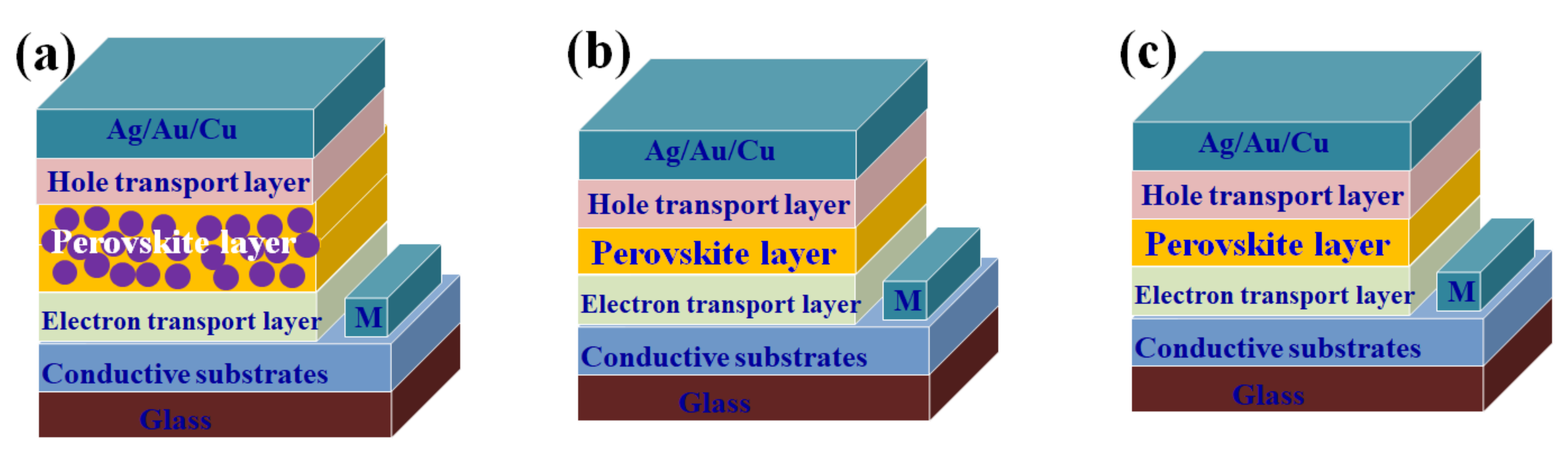
2. Structure of PSCs
3. Introduction of QDs
4. QD-Modified Interface Layer
4.1. QD-Modified Perovskite/ETL Interface
4.1.1. CQD-Modified Perovskite/ETL Interface
4.1.2. GQD-Modified Perovskite/ETL Interface
4.1.3. PQD-Modified Perovskite/ETL Interface
4.1.4. Other-QD-Modified Perovskite/ETL Interface

4.2. QD-Modified Perovskite/HTL Interface
4.2.1. CQD- and GQD-Modified Perovskite/HTL Interface
4.2.2. PQD-Modified Perovskite/HTL Interface
4.2.3. Other-QD-Modified Perovskite/HTL Interface


| QDs | Size | Device Structure | Voc | Jsc | FF % | PCE % | Ref. |
|---|---|---|---|---|---|---|---|
| CdTe | 10~20 nm | ITO/SnO2/FA0.57MA0.43PbIxBryCl3−x−y/ CdTe QDs/Spiro-OMeTAD/Au | 1.05 | 23.46 | 72 | 17.87 | [120] |
| CdSe/CsPbI3 | ~3 nm | FTO/TiO2/MAPbI3/ CdSe/CsPbI3 QDs/ Spiro-OMeTAD/Au | 0.976 | 24.60 | 71 | 17.10 | [121] |
| MoS2 | ~2.6 nm | FTO/c-TiO2/m-TiO2/MAPbI3/MoS2 QDs:Reduced graphene oxide/ Spiro-OMeTAD/Au | 1.11 | 22.81 | 80 | 20.12 | [115] |
| PbS | ~3.4 nm | FTO/c-TiO2/MAPbI3/PbS QDs/ Spiro-OMeTAD/Au | 1.14 | 23.17 | 72.83 | 19.24 | [113] |
| PbSO4(PbO)4 | 2~5 nm | FTO/c-TiO2/m-TiO2/CH3NH3PbI3/ PbSO4(PbO)4 QDs/ Spiro-OMeTAD/Au | 1.10 | 24.27 | 75 | 20.02 | [123] |
| Black Phosphorus | ~5.2 nm | ITO/PEDOT:PSS/BP QDs/MAPbI3/PCBM/Ag | 1.01 | 20.13 | 80 | 16.69 | [122] |
5. Summary
Author Contributions
Funding
Institutional Review Board Statement
Informed Consent Statement
Data Availability Statement
Acknowledgments
Conflicts of Interest
References
- Heo, J.H.; Song, D.H.; Patil, B.R.; Im, S.H. Recent Progress of Innovative Perovskite Hybrid Solar Cells. Isr. J. Chem. 2015, 55, 966–977. [Google Scholar] [CrossRef]
- Moore, K.; Wei, W. Applications of carbon nanomaterials in perovskite solar cells for solar energy conversion. Nano Mater. Sci. 2021, 3, 276–290. [Google Scholar] [CrossRef]
- Vakulchuk, R.; Overland, I.; Scholten, D. Renewable energy and geopolitics: A review. Renew. Sustain. Energy Rev. 2020, 122, 109547. [Google Scholar] [CrossRef]
- Kabir, E.; Kumar, P.; Kumar, S.; Adelodun, A.A.; Kim, K.-H. Solar energy: Potential and future prospects. Renew. Sustain. Energy Rev. 2018, 82, 894–900. [Google Scholar] [CrossRef]
- Ma, T.; Li, S.; Gu, W.; Weng, S.; Peng, J.; Xiao, G. Solar energy harvesting pavements on the road: Comparative study and performance assessment. Sustain. Cities Soc. 2022, 81, 103868. [Google Scholar] [CrossRef]
- Chi, W.; Banerjee, S.K. Development of perovskite solar cells by incorporating quantum dots. Chem. Eng. J. 2021, 426, 131588. [Google Scholar] [CrossRef]
- Sharmoukh, W.; Al Kiey, S.A.; Ali, B.A.; Menon, L.; Allam, N.K. Recent progress in the development of hole-transport materials to boost the power conversion efficiency of perovskite solar cells. Sustain. Mater. Technol. 2020, 26, e00210. [Google Scholar] [CrossRef]
- Kim, G.-H.; Kim, D.S. Development of perovskite solar cells with >25% conversion efficiency. Joule 2021, 5, 1033–1035. [Google Scholar] [CrossRef]
- Chao, L.; Niu, T.; Gao, W.; Ran, C.; Song, L.; Chen, Y.; Huang, W. Solvent Engineering of the Precursor Solution toward Large-Area Production of Perovskite Solar Cells. Adv. Mater. 2021, 33, 2005410. [Google Scholar] [CrossRef]
- Mesquita, I.; Andrade, L.; Mendes, A. Perovskite solar cells: Materials, configurations and stability. Renew. Sustain. Energy Rev. 2018, 82, 2471–2489. [Google Scholar] [CrossRef]
- Ren, K.; Huang, L.; Yue, S.; Lu, S.; Liu, K.; Azam, M.; Wang, Z.; Wei, Z.; Qu, S.; Wang, Z. Turning a disadvantage into an advantage: Synthesizing high-quality organometallic halide perovskite nanosheet arrays for humidity sensors. J. Mater. Chem. C 2017, 5, 2504–2508. [Google Scholar] [CrossRef]
- Sriabisha, R.; Hariharan, R. High efficiency perovskite solar cell. Mater. Today Proc. 2020, 33, 450–453. [Google Scholar] [CrossRef]
- Boyd, C.C.; Cheacharoen, R.; Leijtens, T.; McGehee, M.D. Understanding Degradation Mechanisms and Improving Stability of Perovskite Photovoltaics. Chem. Rev. 2019, 119, 3418–3451. [Google Scholar] [CrossRef]
- Niu, G.; Guo, X.; Wang, L. Review of recent progress in chemical stability of perovskite solar cells. J. Mater. Chem. A 2015, 3, 8970–8980. [Google Scholar] [CrossRef]
- Rakstys, K.; Igci, C.; Nazeeruddin, M.K. Efficiency vs. stability: Dopant-free hole transporting materials towards stabilized perovskite solar cells. Chem. Sci. 2019, 10, 6748–6769. [Google Scholar] [CrossRef] [Green Version]
- Zhang, H.; Ren, X.; Chen, X.; Mao, J.; Cheng, J.; Zhao, Y.; Liu, Y.; Milic, J.; Yin, W.-J.; Grätzel, M.; et al. Improving the stability and performance of perovskite solar cells via off-the-shelf post-device ligand treatment. Energy Environ. Sci. 2018, 11, 2253–2262. [Google Scholar] [CrossRef]
- Bae, S.; Kim, S.; Lee, S.-W.; Cho, K.J.; Park, S.; Lee, S.; Kang, Y.; Lee, H.-S.; Kim, D. Electric-Field-Induced Degradation of Methylammonium Lead Iodide Perovskite Solar Cells. J. Phys. Chem. Lett. 2016, 7, 3091–3096. [Google Scholar] [CrossRef]
- Li, R.; Ding, J.; Mu, X.; Kang, Y.; Wang, A.; Bi, W.; Zhang, Y.; Cao, J.; Dong, Q. Hyperbranched phthalocyanine enabling black-phase formamidinium perovskite solar cells processing and operating in humidity open air. J. Energy Chem. 2022, 71, 141–149. [Google Scholar] [CrossRef]
- Mohsseni, M.; Majles Ara, M.H.; Dehghani, M. Determination of critical total secondary phase densities in CZTS and investigation of their effects on the perovskite solar cell performance with CZTS as an HTL. Opt. Mater. 2022, 128, 112453. [Google Scholar] [CrossRef]
- Ripolles, T.S.; Nishinaka, K.; Ogomi, Y.; Miyata, Y.; Hayase, S. Efficiency enhancement by changing perovskite crystal phase and adding a charge extraction interlayer in organic amine free-perovskite solar cells based on cesium. Sol. Energy Mater. Sol. Cells 2016, 144, 532–536. [Google Scholar] [CrossRef]
- Kari, M.; Saghafi, K. Current-voltage hysteresis reduction of CH3NH3PbI3 planar perovskite solar cell by multi-layer absorber. Micro Nanostruct. 2022, 165, 207207. [Google Scholar] [CrossRef]
- Lin, Z. Relationship between ion vacancy mobility and hysteresis of perovskite solar cells. Chem. Phys. 2022, 554, 111422. [Google Scholar] [CrossRef]
- Wu, F.; Pathak, R.; Qiao, Q. Origin and alleviation of J-V hysteresis in perovskite solar cells: A short review. Catal. Today 2021, 374, 86–101. [Google Scholar] [CrossRef]
- Zhu, Z.; Ma, J.; Wang, Z.; Mu, C.; Fan, Z.; Du, L.; Bai, Y.; Fan, L.; Yan, H.; Phillips, D.L.; et al. Efficiency enhancement of perovskite solar cells through fast electron extraction: The role of graphene quantum dots. J. Am. Chem. Soc. 2014, 136, 3760–3763. [Google Scholar] [CrossRef]
- Ryu, J.; Lee, J.W.; Yu, H.; Yun, J.; Lee, K.; Lee, J.; Hwang, D.; Kang, J.; Kim, S.K.; Jang, J. Size effects of a graphene quantum dot modified-blocking TiO2 layer for efficient planar perovskite solar cells. J. Mater. Chem. A 2017, 5, 16834–16842. [Google Scholar] [CrossRef]
- Duan, J.; Zhao, Y.; He, B.; Tang, Q. High-Purity Inorganic Perovskite Films for Solar Cells with 9.72% Efficiency. Angew. Chem. Int. Ed. Engl. 2018, 57, 3787–3791. [Google Scholar] [CrossRef]
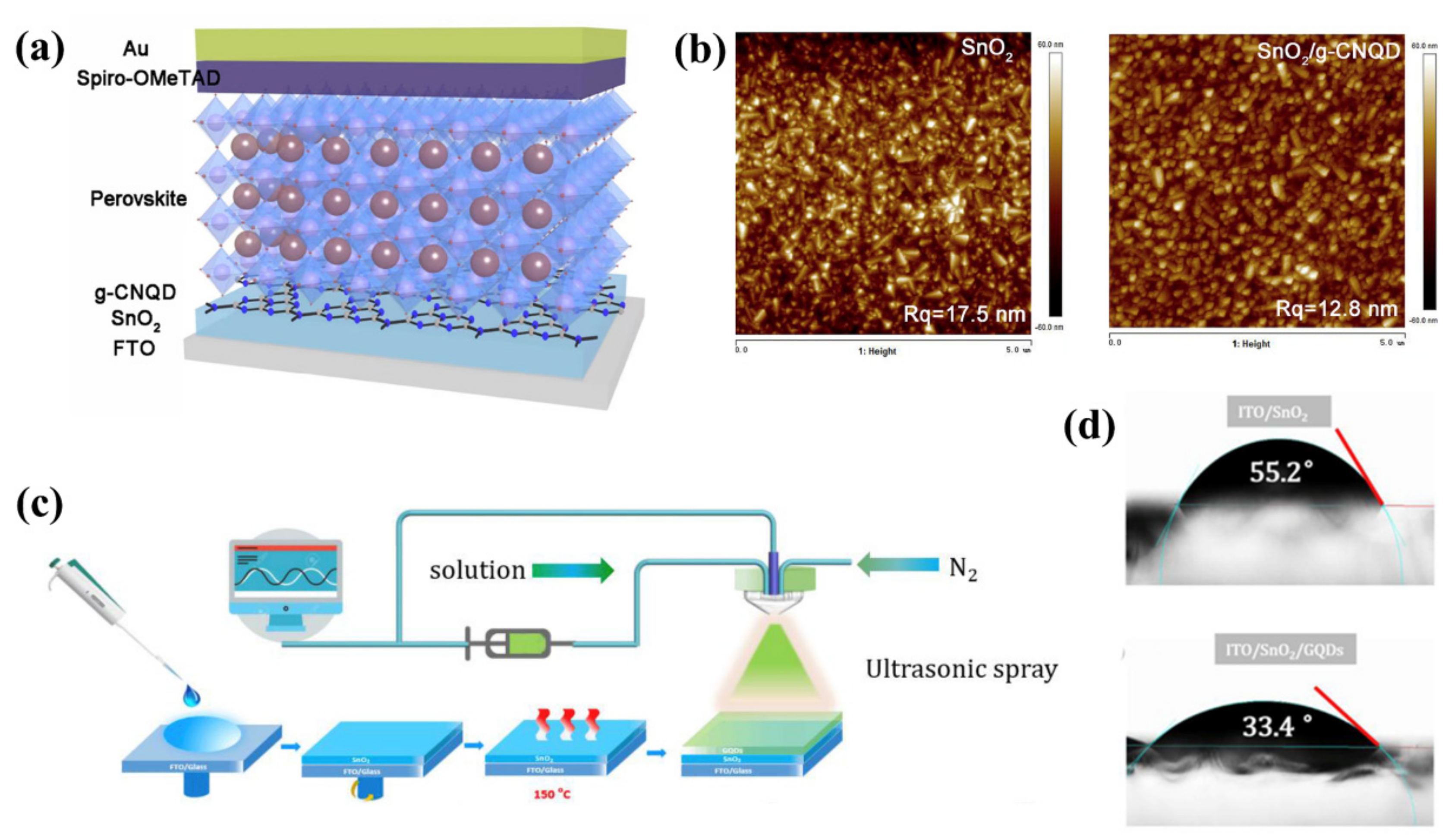
- Xia, H.; Ma, Z.; Xiao, Z.; Zhou, W.; Zhang, H.; Du, C.; Zhuang, J.; Cheng, X.; Liu, X.; Huang, Y. Interfacial modification using ultrasonic atomized graphene quantum dots for efficient perovskite solar cells. Org. Electron. 2019, 75, 105415. [Google Scholar] [CrossRef]
- Jin, J.; Chen, C.; Li, H.; Cheng, Y.; Xu, L.; Dong, B.; Song, H.; Dai, Q. Enhanced Performance and Photostability of Perovskite Solar Cells by Introduction of Fluorescent Carbon Dots. ACS Appl. Mater. Interfaces 2017, 9, 14518–14524. [Google Scholar] [CrossRef]
- Li, H.; Shi, W.; Huang, W.; Yao, E.P.; Han, J.; Chen, Z.; Liu, S.; Shen, Y.; Wang, M.; Yang, Y. Carbon Quantum Dots/TiOx Electron Transport Layer Boosts Efficiency of Planar Heterojunction Perovskite Solar Cells to 19. Nano Lett. 2017, 17, 2328–2335. [Google Scholar] [CrossRef]
- Xie, J.; Huang, K.; Yu, X.; Yang, Z.; Xiao, K.; Qiang, Y.; Zhu, X.; Xu, L.; Wang, P.; Cui, C.; et al. Enhanced Electronic Properties of SnO2 via Electron Transfer from Graphene Quantum Dots for Efficient Perovskite Solar Cells. ACS Nano 2017, 11, 9176–9182. [Google Scholar] [CrossRef]
- Yang, Z.; Xie, J.; Arivazhagan, V.; Xiao, K.; Qiang, Y.; Huang, K.; Hu, M.; Cui, C.; Yu, X.; Yang, D. Efficient and highly light stable planar perovskite solar cells with graphene quantum dots doped PCBM electron transport layer. Nano Energy 2017, 40, 345–351. [Google Scholar] [CrossRef]
- Liu, H.; Chen, Z.; Wang, H.; Ye, F.; Ma, J.; Zheng, X.; Gui, P.; Xiong, L.; Wen, J.; Fang, G. A facile room temperature solution synthesis of SnO2 quantum dots for perovskite solar cells. J. Mater. Chem. A 2019, 7, 10636–10643. [Google Scholar] [CrossRef]
- Wang, E.; Chen, P.; Yin, X.; Wu, Y.; Que, W. Tailoring Electronic Properties of SnO2 Quantum Dots via Aluminum Addition for High-Efficiency Perovskite Solar Cells. Sol. RRL 2019, 3, 1900041. [Google Scholar] [CrossRef]
- Vijayaraghavan, S.N.; Wall, J.; Li, L.; Xing, G.; Zhang, Q.; Yan, F. Low-temperature processed highly efficient hole transport layer free carbon-based planar perovskite solar cells with SnO2 quantum dot electron transport layer. Mater. Today Phys. 2020, 13, 100204. [Google Scholar] [CrossRef]
- Wang, E.; Chen, P.; Yin, X.; Wu, Y.; Que, W. Novel ethanol vapor annealing treatment of SnO2 quantum dots film for highly efficient planar heterojunction perovskite solar cells. Org. Electron. 2020, 84, 105751. [Google Scholar] [CrossRef]
- Park, S.Y.; Baek, M.Y.; Ju, Y.; Kim, D.H.; Moon, C.S.; Noh, J.H.; Jung, H.S. Simultaneous Ligand Exchange Fabrication of Flexible Perovskite Solar Cells using Newly Synthesized Uniform Tin Oxide Quantum Dots. J. Phys. Chem. Lett. 2018, 9, 5460–5467. [Google Scholar] [CrossRef]
- Remya, V.R.; Prajitha, V.; George, J.S.; Jibin, K.P.; Thomas, S. Chapter 7—Quantum dots: A brief introduction. In Nanoscale Processing; Thomas, S., Balakrishnan, P., Eds.; Elsevier: Amsterdam, The Netherlands, 2021; pp. 181–196. [Google Scholar]
- Alami, A.H.; Faraj, M. Quantum Dots: Types and Characteristics. In Encyclopedia of Smart Materials; Olabi, A.-G., Ed.; Elsevier: Oxford, UK, 2022; pp. 183–191. [Google Scholar]
- Paulo, S.; Stoica, G.; Cambarau, W.; Martinez-Ferrero, E.; Palomares, E. Carbon quantum dots as new hole transport material for perovskite solar cells. Synth. Met. 2016, 222, 17–22. [Google Scholar] [CrossRef]
- Zou, H.; Guo, D.; He, B.; Yu, J.; Fan, K. Enhanced photocurrent density of HTM-free perovskite solar cells by carbon quantum dots. Appl. Surf. Sci. 2018, 430, 625–631. [Google Scholar] [CrossRef]
- Yuan, J.; Ling, X.; Yang, D.; Li, F.; Zhou, S.; Shi, J.; Qian, Y.; Hu, J.; Sun, Y.; Yang, Y.; et al. Band-Aligned Polymeric Hole Transport Materials for Extremely Low Energy Loss α-CsPbI3 Perovskite Nanocrystal Solar Cells. Joule 2018, 2, 2450–2463. [Google Scholar] [CrossRef] [Green Version]
- Kim, J.-Y.; Baek, W.; Kim, S.; Kang, G.; Han, I.K.; Hyeon, T.; Park, M. Moisture proof hole transport layers based on CISe quantum dots for highly stable and large active area perovskite solar cells. Appl. Surf. Sci. 2019, 496, 143610. [Google Scholar] [CrossRef]
- Yang, L.; Li, Y.; Wang, L.; Pei, Y.; Wang, Z.; Zhang, Y.; Lin, H.; Li, X. Exfoliated Fluorographene Quantum Dots as Outstanding Passivants for Improved Flexible Perovskite Solar Cells. ACS Appl. Mater. Interfaces 2020, 12, 22992–23001. [Google Scholar] [CrossRef] [PubMed]
- Lv, Z.; He, L.; Jiang, H.; Ma, X.; Wang, F.; Fan, L.; Wei, M.; Yang, J.; Yang, L.; Yang, N. Diluted-CdS Quantum Dot-Assisted SnO2 Electron Transport Layer with Excellent Conductivity and Suitable Band Alignment for High-Performance Planar Perovskite Solar Cells. ACS Appl. Mater. Interfaces 2021, 13, 16326–16335. [Google Scholar] [CrossRef] [PubMed]
- Zheng, J.; Li, F.; Chen, C.; Du, Q.; Jin, M.; Li, H.; Ji, M.; Shen, Z. Perovskite Solar Cells Employing a PbSO4(PbO)4 Quantum Dot-Doped Spiro-OMeTAD Hole Transport Layer with an Efficiency over 22%. ACS Appl. Mater. Interfaces 2022, 14, 2989–2999. [Google Scholar] [CrossRef]
- Kim, E.-B.; Akhtar, M.S.; Shin, H.-S.; Ameen, S.; Nazeeruddin, M.K. A review on two-dimensional (2D) and 2D-3D multidimensional perovskite solar cells: Perovskites structures, stability, and photovoltaic performances. J. Photochem. Photobiol. C Photochem. Rev. 2021, 48, 100405. [Google Scholar] [CrossRef]
- Hernández-Balaguera, E.; Arredondo, B.; Pozo, G.d.; Romero, B. Exploring the impact of fractional-order capacitive behavior on the hysteresis effects of perovskite solar cells: A theoretical perspective. Commun. Nonlinear Sci. Numer. Simul. 2020, 90, 105371. [Google Scholar] [CrossRef]
- Zhang, F.; Zhu, K. Additive Engineering for Efficient and Stable Perovskite Solar Cells. Adv. Energy Mater. 2020, 10, 1902579. [Google Scholar] [CrossRef]
- Chen, J.; Park, N.-G. Causes and Solutions of Recombination in Perovskite Solar Cells. Adv. Mater. 2019, 31, 1803019. [Google Scholar] [CrossRef]
- Gan, X.; Yang, S.; Zhang, J.; Wang, G.; He, P.; Sun, H.; Yuan, H.; Yu, L.; Ding, G.; Zhu, Y. Graphite-N Doped Graphene Quantum Dots as Semiconductor Additive in Perovskite Solar Cells. ACS Appl. Mater. Interfaces 2019, 11, 37796–37803. [Google Scholar] [CrossRef]
- Benetti, D.; Jokar, E.; Yu, C.-H.; Fathi, A.; Zhao, H.; Vomiero, A.; Wei-Guang Diau, E.; Rosei, F. Hole-extraction and photostability enhancement in highly efficient inverted perovskite solar cells through carbon dot-based hybrid material. Nano Energy 2019, 62, 781–790. [Google Scholar] [CrossRef]
- Wang, Z.; Rong, X.; Wang, L.; Wang, W.; Lin, H.; Li, X. Dual Role of Amino-Functionalized Graphene Quantum Dots in NiOx Films for Efficient Inverted Flexible Perovskite Solar Cells. ACS Appl. Mater. Interfaces 2020, 12, 8342–8350. [Google Scholar] [CrossRef]
- Khanzada, L.S.; Levchuk, I.; Hou, Y.; Azimi, H.; Osvet, A.; Ahmad, R.; Brandl, M.; Herre, P.; Distaso, M.; Hock, R.; et al. Effective Ligand Engineering of the Cu2ZnSnS4 Nanocrystal Surface for Increasing Hole Transport Efficiency in Perovskite Solar Cells. Adv. Funct. Mater. 2016, 26, 8300–8306. [Google Scholar] [CrossRef]
- Guo, Q.; Yuan, F.; Zhang, B.; Zhou, S.; Zhang, J.; Bai, Y.; Fan, L.; Hayat, T.; Alsaedi, A.; Tan, Z.a. Passivation of the grain boundaries of CH3NH3PbI3 using carbon quantum dots for highly efficient perovskite solar cells with excellent environmental stability. Nanoscale 2019, 11, 115–124. [Google Scholar] [CrossRef]
- Zhou, Q.; Tang, S.; Yuan, G.; Zhu, W.; Huang, Y.; Li, S.; Lin, M. Tailored graphene quantum dots to passivate defects and accelerate charge extraction for all-inorganic CsPbIBr2 perovskite solar cells. J. Alloys Compd. 2022, 895, 162529. [Google Scholar] [CrossRef]
- Wang, B.; Li, B.; Shen, T.; Li, M.; Tian, J. ZnSe quantum dots downshifting layer for perovskite solar cells. J. Energy Chem. 2018, 27, 736–741. [Google Scholar] [CrossRef] [Green Version]
- Wang, Q.; Zhang, X.; Jin, Z.; Zhang, J.; Gao, Z.; Li, Y.; Liu, S.F. Energy-Down-Shift CsPbCl3:Mn Quantum Dots for Boosting the Efficiency and Stability of Perovskite Solar Cells. ACS Energy Lett. 2017, 2, 1479–1486. [Google Scholar] [CrossRef]
- Ye, M.; Gong, J.; Lai, Y.; Lin, C.; Lin, Z. High-Efficiency Photoelectrocatalytic Hydrogen Generation Enabled by Palladium Quantum Dots-Sensitized TiO2 Nanotube Arrays. J. Am. Chem. Soc. 2012, 134, 15720–15723. [Google Scholar] [CrossRef]
- Xu, Y.-F.; Yang, M.-Z.; Chen, B.-X.; Wang, X.-D.; Chen, H.-Y.; Kuang, D.-B.; Su, C.-Y. A CsPbBr3 Perovskite Quantum Dot/Graphene Oxide Composite for Photocatalytic CO2 Reduction. J. Am. Chem. Soc. 2017, 139, 5660–5663. [Google Scholar] [CrossRef]
- Zhang, S.; Liu, X.; Liu, C.; Luo, S.; Wang, L.; Cai, T.; Zeng, Y.; Yuan, J.; Dong, W.; Pei, Y.; et al. MoS2 Quantum Dot Growth Induced by S Vacancies in a ZnIn2S4 Monolayer: Atomic-Level Heterostructure for Photocatalytic Hydrogen Production. ACS Nano 2018, 12, 751–758. [Google Scholar] [CrossRef]
- Zhang, X.; Zeng, Q.; Xiong, Y.; Ji, T.; Wang, C.; Shen, X.; Lu, M.; Wang, H.; Wen, S.; Zhang, Y.; et al. Energy Level Modification with Carbon Dot Interlayers Enables Efficient Perovskite Solar Cells and Quantum Dot Based Light-Emitting Diodes. Adv. Funct. Mater. 2020, 30, 1910530. [Google Scholar] [CrossRef]
- Zheng, Z.; Zhuge, F.; Wang, Y.; Zhang, J.; Gan, L.; Zhou, X.; Li, H.; Zhai, T. Decorating Perovskite Quantum Dots in TiO2 Nanotubes Array for Broadband Response Photodetector. Adv. Funct. Mater. 2017, 27, 1703115. [Google Scholar] [CrossRef]
- Lu, J.; Sheng, X.; Tong, G.; Yu, Z.; Sun, X.; Yu, L.; Xu, X.; Wang, J.; Xu, J.; Shi, Y.; et al. Ultrafast Solar-Blind Ultraviolet Detection by Inorganic Perovskite CsPbX3 Quantum Dots Radial Junction Architecture. Adv. Mater. 2017, 29, 1700400. [Google Scholar] [CrossRef]
- Li, X.; Wu, Y.; Zhang, S.; Cai, B.; Gu, Y.; Song, J.; Zeng, H. CsPbX3 Quantum Dots for Lighting and Displays: Room-Temperature Synthesis, Photoluminescence Superiorities, Underlying Origins and White Light-Emitting Diodes. Adv. Funct. Mater. 2016, 26, 2435–2445. [Google Scholar] [CrossRef]
- Wu, K.; Liang, G.; Shang, Q.; Ren, Y.; Kong, D.; Lian, T. Ultrafast Interfacial Electron and Hole Transfer from CsPbBr3 Perovskite Quantum Dots. J. Am. Chem. Soc. 2015, 137, 12792–12795. [Google Scholar] [CrossRef]
- Yuan, F.; He, P.; Xi, Z.; Li, X.; Li, Y.; Zhong, H.; Fan, L.; Yang, S. Highly efficient and stable white LEDs based on pure red narrow bandwidth emission triangular carbon quantum dots for wide-color gamut backlight displays. Nano Res. 2019, 12, 1669–1674. [Google Scholar] [CrossRef]
- Tu, Y.; Wu, J.; Zheng, M.; Huo, J.; Zhou, P.; Lan, Z.; Lin, J.; Huang, M. TiO2 quantum dots as superb compact block layers for high-performance CH3NH3PbI3 perovskite solar cells with an efficiency of 16.97%. Nanoscale 2015, 7, 20539–20546. [Google Scholar] [CrossRef]
- Tavakoli, M.M.; Tavakoli, R.; Nourbakhsh, Z.; Waleed, A.; Virk, U.S.; Fan, Z. High Efficiency and Stable Perovskite Solar Cell Using ZnO/rGO QDs as an Electron Transfer Layer. Adv. Mater. Interfaces 2016, 3, 1500790. [Google Scholar] [CrossRef]
- Jaffri, S.B.; Ahmad, K.S. Interfacial engineering revolutionizers: Perovskite nanocrystals and quantum dots accentuated performance enhancement in perovskite solar cells. Crit. Rev. Solid State Mater. Sci. 2021, 46, 251–279. [Google Scholar] [CrossRef]
- He, C.; Wang, Z.L. Triboelectric nanogenerator as a new technology for effective PM2.5 removing with zero ozone emission. Prog. Nat. Sci. Mater. Int. 2018, 28, 99–112. [Google Scholar] [CrossRef]
- Guo, R.; Zeng, D.; Xie, Y.; Ling, Y.; Zhou, D.; Jiang, L.; Jiao, W.; Zhao, J.; Li, S. Carbon nitride quantum dots (CNQDs)/TiO2 nanoparticle heterojunction photocatalysts for enhanced ultraviolet-visible-light-driven bisphenol a degradation and H2 production. Int. J. Hydrogen Energy 2020, 45, 22534–22544. [Google Scholar] [CrossRef]
- Chandra, S.; Pathan, S.H.; Mitra, S.; Modha, B.H.; Goswami, A.; Pramanik, P. Tuning of photoluminescence on different surface functionalized carbon quantum dots. RSC Adv. 2012, 2, 3602–3606. [Google Scholar] [CrossRef]
- Nekoueian, K.; Amiri, M.; Sillanpää, M.; Marken, F.; Boukherroub, R.; Szunerits, S. Carbon-based quantum particles: An electroanalytical and biomedical perspective. Chem. Soc. Rev. 2019, 48, 4281–4316. [Google Scholar] [CrossRef]
- Tang, D.; Zhang, H.; Huang, H.; Liu, R.; Han, Y.; Liu, Y.; Tong, C.; Kang, Z. Carbon quantum dots enhance the photocatalytic performance of BiVO4 with different exposed facets. Dalton Trans. 2013, 42, 6285–6289. [Google Scholar] [CrossRef]
- Liu, Y.; Yu, Y.-X.; Zhang, W.-D. Carbon quantum dots-doped CdS microspheres with enhanced photocatalytic performance. J. Alloys Compd. 2013, 569, 102–110. [Google Scholar] [CrossRef]
- Ding, J.; Zhao, Y.; Duan, J.; He, B.; Tang, Q. Alloy-Controlled Work Function for Enhanced Charge Extraction in All-Inorganic CsPbBr3 Perovskite Solar Cells. ChemSusChem 2018, 11, 1432–1437. [Google Scholar] [CrossRef]
- Liu, P.; Sun, Y.; Wang, S.; Zhang, H.; Gong, Y.; Li, F.; Shi, Y.; Du, Y.; Li, X.; Guo, S.-S.; et al. Two dimensional graphitic carbon nitride quantum dots modified perovskite solar cells and photodetectors with high performances. J. Power Sources 2020, 451, 227825. [Google Scholar] [CrossRef]
- Chen, H.; Luo, Q.; Liu, T.; Tai, M.; Lin, J.; Murugadoss, V.; Lin, H.; Wang, J.; Guo, Z.; Wang, N. Boosting Multiple Interfaces by Co-Doped Graphene Quantum Dots for High Efficiency and Durability Perovskite Solar Cells. ACS Appl. Mater. Interfaces 2020, 12, 13941–13949. [Google Scholar] [CrossRef]
- Gao, Z.W.; Wang, Y.; Liu, H.; Sun, J.; Kim, J.; Li, Y.; Xu, B.; Choy, W.C.H. Tailoring the Interface in FAPbI3 Planar Perovskite Solar Cells by Imidazole—Graphene—Quantum—Dots. Adv. Funct. Mater. 2021, 31, 2101438. [Google Scholar] [CrossRef]
- Irannejad, N.; Rezaei, B.; Ensafi, A.A. Upconversion graphene quantum dots incorporation in performance enhancement of p-i-n perovskite solar cells. J. Environ. Chem. Eng. 2021, 9, 106898. [Google Scholar] [CrossRef]
- Jindal, S.; Giripunje, S.M. An insight into electronic and optical properties of multilayer graphene quantum dots synthesized by hydrothermal approach. Synth. Met. 2018, 239, 36–42. [Google Scholar] [CrossRef]
- Liu, Q.; Zhang, J.; He, H.; Huang, G.; Xing, B.; Jia, J.; Zhang, C. Green Preparation of High Yield Fluorescent Graphene Quantum Dots from Coal-Tar-Pitch by Mild Oxidation. Nanomaterials 2018, 8, 844. [Google Scholar] [CrossRef] [Green Version]
- Zhang, X.; Wang, Q.; Jin, Z.; Chen, Y.; Liu, H.; Wang, J.; Li, Y.; Liu, S. Graphdiyne Quantum Dots for Much Improved Stability and Efficiency of Perovskite Solar Cells. Adv. Mater. Interfaces 2018, 5, 1701117. [Google Scholar] [CrossRef]
- Zheng, X.; Troughton, J.; Gasparini, N.; Lin, Y.; Wei, M.; Hou, Y.; Liu, J.; Song, K.; Chen, Z.; Yang, C.; et al. Quantum Dots Supply Bulk- and Surface-Passivation Agents for Efficient and Stable Perovskite Solar Cells. Joule 2019, 3, 1963–1976. [Google Scholar] [CrossRef]
- Yang, W.; Su, R.; Luo, D.; Hu, Q.; Zhang, F.; Xu, Z.; Wang, Z.; Tang, J.; Lv, Z.; Yang, X.; et al. Surface modification induced by perovskite quantum dots for triple-cation perovskite solar cells. Nano Energy 2020, 67, 104189. [Google Scholar] [CrossRef]
- Wang, H.; Song, Y.; Dang, S.; Jiang, N.; Feng, J.; Tian, W.; Dong, Q. Reducing Photovoltage Loss in Inverted Perovskite Solar Cells by Quantum Dots Alloying Modification at Cathode Contact. Sol. RRL 2019, 4, 1900468. [Google Scholar] [CrossRef]
- Yang, Y.; Wang, W. Effects of incorporating PbS quantum dots in perovskite solar cells based on CH3NH3PbI3. J. Power Sources 2015, 293, 577–584. [Google Scholar] [CrossRef] [Green Version]
- Turner, D.B.; Hassan, Y.; Scholes, G.D. Exciton Superposition States in CdSe Nanocrystals Measured Using Broadband Two-Dimensional Electronic Spectroscopy. Nano Lett. 2012, 12, 880–886. [Google Scholar] [CrossRef]
- Chen, L.; Bao, H.; Tan, T.; Prezhdo, O.V.; Ruan, X. Shape and Temperature Dependence of Hot Carrier Relaxation Dynamics in Spherical and Elongated CdSe Quantum Dots. J. Phys. Chem. C 2011, 115, 11400–11406. [Google Scholar] [CrossRef]
- Magaryan, K.A.; Karimullin, K.R.; Vasil’eva, I.A.; Naumov, A.V. Analysis of the Temperature Dependence of the Exciton Luminescence Spectra of Cadmium Selenide Quantum Dots Grown in a Liquid Crystal Matrix. Opt. Spectrosc. 2019, 126, 41–43. [Google Scholar] [CrossRef]
- Prodanović, N.; Vukmirović, N.; Ikonić, Z.; Harrison, P.; Indjin, D. Importance of Polaronic Effects for Charge Transport in CdSe Quantum Dot Solids. J. Phys. Chem. Lett. 2014, 5, 1335–1340. [Google Scholar] [CrossRef] [PubMed]
- Mueller, M.L.; Yan, X.; Dragnea, B.; Li, L.-S. Slow Hot-Carrier Relaxation in Colloidal Graphene Quantum Dots. Nano Lett. 2011, 11, 56–60. [Google Scholar] [CrossRef] [PubMed]
- Ali, S.M.; Ramay, S.M.; Aziz, M.H.; ur-Rehman, N.; AlGarawi, M.S.; AlGhamd, S.S.; Mahmood, A.; Alkhuraiji, T.S.; Atiq, S. Efficiency enhancement of perovskite solar cells by incorporation of CdS quantum dot through fast electron injection. Org. Electron. 2018, 62, 21–25. [Google Scholar] [CrossRef]
- Yenel, E. Synthesis and application of colloidal CdS quantum dots as interface modification material in perovskite solar cells. Turk. J. Chem. 2021, 45, 1952–1958. [Google Scholar] [CrossRef]
- Hanmandlu, C.; Swamy, S.; Singh, A.; Hsin-An, C.; Liu, C.-C.; Lai, C.-S.; Mohapatra, A.; Pao, C.-W.; Chen, P.; Chu, C.-W. Suppression of surface defects to achieve hysteresis-free inverted perovskite solar cells via quantum dot passivation. J. Mater. Chem. A 2020, 8, 5263–5274. [Google Scholar] [CrossRef]
- Gao, F.; Dai, H.; Pan, H.; Chen, Y.; Wang, J.; Chen, Z. Performance enhancement of perovskite solar cells by employing TiO2 nanorod arrays decorated with CuInS2 quantum dots. J. Colloid Interface Sci. 2018, 513, 693–699. [Google Scholar] [CrossRef]
- Gao, F.; Zheng, Q.; Zhang, Y. Stability Improvement of Perovskite Solar Cells for Application of CuInS2 Quantum Dot-Modified TiO2 Nanoarrays. ACS Omega 2019, 4, 3432–3438. [Google Scholar] [CrossRef] [Green Version]
- He, M.; Pang, X.; Liu, X.; Jiang, B.; He, Y.; Snaith, H.; Lin, Z. Monodisperse Dual-Functional Upconversion Nanoparticles Enabled Near-Infrared Organolead Halide Perovskite Solar Cells. Angew. Chem. Int. Ed. Engl. 2016, 55, 4280–4284. [Google Scholar] [CrossRef]
- Qi, J.; Xiong, H.; Wang, G.; Xie, H.; Jia, W.; Zhang, Q.; Li, Y.; Wang, H. High-performance solar cells with induced crystallization of perovskite by an evenly distributed CdSe quantum dots seed-mediated underlayer. J. Power Sources 2018, 376, 46–54. [Google Scholar] [CrossRef]
- Zhou, S.; Tang, R.; Yin, L. Slow-Photon-Effect-Induced Photoelectrical-Conversion Efficiency Enhancement for Carbon-Quantum-Dot-Sensitized Inorganic CsPbBr3 Inverse Opal Perovskite Solar Cells. Adv. Mater. 2017, 29, 1703682. [Google Scholar] [CrossRef]
- Wei, X.; Liu, X.; Liu, H.; Yang, S.; Zeng, H.; Meng, F.; Lei, X.; Liu, J. Exfoliated graphitic carbon nitride self-recognizing CH3NH3PbI3 grain boundaries by hydrogen bonding interaction for improved perovskite solar cells. Sol. Energy 2019, 181, 161–168. [Google Scholar] [CrossRef]
- Khorshidi, E.; Rezaei, B.; Blätte, D.; Buyruk, A.; Reus, M.A.; Hanisch, J.; Böller, B.; Müller-Buschbaum, P.; Ameri, T. Hydrophobic Graphene Quantum Dots for Defect Passivation and Enhanced Moisture Stability of CH3NH3PbI3 Perovskite Solar Cells. Sol. RRL 2022, 2200023. [Google Scholar] [CrossRef]
- Cha, M.; Da, P.; Wang, J.; Wang, W.; Chen, Z.; Xiu, F.; Zheng, G.; Wang, Z.S. Enhancing Perovskite Solar Cell Performance by Interface Engineering Using CH3NH3PbBr0.9I2.1 Quantum Dots. J. Am. Chem. Soc. 2016, 138, 8581–8587. [Google Scholar] [CrossRef] [PubMed]
- Bian, H.; Bai, D.; Jin, Z.; Wang, K.; Liang, L.; Wang, H.; Zhang, J.; Wang, Q.; Liu, S. Graded Bandgap CsPbI2+xBr1+x Perovskite Solar Cells with a Stabilized Efficiency of 14.4%. Joule 2018, 2, 1500–1510. [Google Scholar] [CrossRef] [Green Version]
- Liu, C.; Hu, M.; Zhou, X.; Wu, J.; Zhang, L.; Kong, W.; Li, X.; Zhao, X.; Dai, S.; Xu, B.; et al. Efficiency and stability enhancement of perovskite solar cells by introducing CsPbI3 quantum dots as an interface engineering layer. NPG Asia Mater. 2018, 10, 552–561. [Google Scholar] [CrossRef]
- Han, S.; Zhang, H.; Wang, R.; He, Q. Bidentate ligand modified CsPbI2Br quantum dots as an interface for high-performance carbon-based perovskite solar cells. Mater. Sci. Semicond. Process. 2021, 131, 105847. [Google Scholar] [CrossRef]
- Fatima, K.; Haider, M.I.; Bashir, A.; Qamar, S.; Qureshi, A.A.; Akhter, Z.; Sultan, M. Surface modification of CsPbI2Br for improved performance of inorganic perovskite solar cells. Phys. E Low-Dimens. Syst. Nanostruct. 2022, 142, 115265. [Google Scholar] [CrossRef]
- Zhang, J.; Bai, D.; Jin, Z.; Bian, H.; Wang, K.; Sun, J.; Wang, Q.; Liu, S. 3D–2D–0D Interface Profiling for Record Efficiency All-Inorganic CsPbBrI2 Perovskite Solar Cells with Superior Stability. Adv. Energy Mater. 2018, 8, 1703246. [Google Scholar] [CrossRef]
- Akin, S.; Altintas, Y.; Mutlugun, E.; Sonmezoglu, S. Cesium lead based inorganic perovskite quantum-dots as interfacial layer for highly stable perovskite solar cells with exceeding 21% efficiency. Nano Energy 2019, 60, 557–566. [Google Scholar] [CrossRef]
- Que, M.; Dai, Z.; Yang, H.; Zhu, H.; Zong, Y.; Que, W.; Padture, N.P.; Zhou, Y.; Chen, O. Quantum-Dot-Induced Cesium-Rich Surface Imparts Enhanced Stability to Formamidinium Lead Iodide Perovskite Solar Cells. ACS Energy Lett. 2019, 4, 1970–1975. [Google Scholar] [CrossRef]
- Yao, Y.; Hang, P.; Wang, P.; Xu, L.; Cui, C.; Xie, J.; Xiao, K.; Li, G.; Lin, P.; Liu, S.; et al. CsPbBr3 quantum dots assisted crystallization of solution-processed perovskite films with preferential orientation for high performance perovskite solar cells. Nanotechnology 2019, 31, 085401. [Google Scholar] [CrossRef]
- Zhang, J.; Jin, Z.; Liang, L.; Wang, H.; Bai, D.; Bian, H.; Wang, K.; Wang, Q.; Yuan, N.; Ding, J.; et al. Iodine-Optimized Interface for Inorganic CsPbI2Br Perovskite Solar Cell to Attain High Stabilized Efficiency Exceeding 14%. Adv. Sci. 2018, 5, 1801123. [Google Scholar] [CrossRef] [Green Version]
- Zhu, X.; Cheng, B.; Li, X.; Zhang, J.; Zhang, L. Enhanced efficiency of perovskite solar cells by PbS quantum dot modification. Appl. Surf. Sci. 2019, 487, 32–40. [Google Scholar] [CrossRef]
- Wu, W.; Xu, H.; Liu, G.; Zheng, H.; Pan, X. Introduction of 4-hydroxybenzaldehyde as interface modifier with multidimensional defects passivation effect for high-performance perovskite solar cells. Appl. Surf. Sci. 2021, 570, 151259. [Google Scholar] [CrossRef]
- Najafi, L.; Taheri, B.; Martin-Garcia, B.; Bellani, S.; Di Girolamo, D.; Agresti, A.; Oropesa-Nunez, R.; Pescetelli, S.; Vesce, L.; Calabro, E.; et al. MoS2 Quantum Dot/Graphene Hybrids for Advanced Interface Engineering of a CH3NH3PbI3 Perovskite Solar Cell with an Efficiency of over 20. ACS Nano 2018, 12, 10736–10754. [Google Scholar] [CrossRef] [Green Version]
- Hao, F.; Stoumpos, C.C.; Chang, R.P.H.; Kanatzidis, M.G. Anomalous Band Gap Behavior in Mixed Sn and Pb Perovskites Enables Broadening of Absorption Spectrum in Solar Cells. J. Am. Chem. Soc. 2014, 136, 8094–8099. [Google Scholar] [CrossRef]
- Olthof, S. Research Update: The electronic structure of hybrid perovskite layers and their energetic alignment in devices. APL Mater. 2016, 4, 091502. [Google Scholar] [CrossRef] [Green Version]
- Schulz, P.; Whittaker-Brooks, L.L.; MacLeod, B.A.; Olson, D.C.; Loo, Y.-L.; Kahn, A. Electronic Level Alignment in Inverted Organometal Perovskite Solar Cells. Adv. Mater. Interfaces 2015, 2, 1400532. [Google Scholar] [CrossRef]
- Torres-Herrera, D.M.; Moreno-Romero, P.M.; Cabrera-German, D.; Cortina-Marrero, H.J.; Sotelo-Lerma, M.; Hu, H. Thermal co-evaporated MoOx:Au thin films and its application as anode modifier in perovskite solar cells. Sol. Energy 2020, 206, 136–144. [Google Scholar] [CrossRef]
- Xiao, J.-W.; Ma, S.; Yu, S.; Zhou, C.; Liu, P.; Chen, Y.; Zhou, H.; Li, Y.; Chen, Q. Ligand engineering on CdTe quantum dots in perovskite solar cells for suppressed hysteresis. Nano Energy 2018, 46, 45–53. [Google Scholar] [CrossRef]
- Ge, J.; Li, W.; He, X.; Chen, H.; Fang, W.; Du, X.; Li, Y.; Zhao, L. Hybrid CdSe/CsPbI3 quantum dots for interface engineering in perovskite solar cells. Sustain. Energy Fuels 2020, 4, 1837–1843. [Google Scholar] [CrossRef]
- Chen, W.; Li, K.; Wang, Y.; Feng, X.; Liao, Z.; Su, Q.; Lin, X.; He, Z. Black Phosphorus Quantum Dots for Hole Extraction of Typical Planar Hybrid Perovskite Solar Cells. J. Phys. Chem. Lett. 2017, 8, 591–598. [Google Scholar] [CrossRef]
- Chen, C.; Li, F.; Zhu, L.; Shen, Z.; Weng, Y.; Lou, Q.; Tan, F.; Yue, G.; Huang, Q.; Wang, M. Efficient and stable perovskite solar cells thanks to dual functions of oleyl amine-coated PbSO4(PbO)4 quantum dots: Defect passivation and moisture/oxygen blocking. Nano Energy 2020, 68, 104313. [Google Scholar] [CrossRef]

| QDs | Size | Device Structure | Voc | Jsc | FF % | PCE % | Ref. |
|---|---|---|---|---|---|---|---|
| CQDs | ~ | FTO/c-TiO2/m-TiO2/CQDs/ CsPbBr3/carbon:PtNi NWS | 1.43 | 6.78 | 80.9 | 7.86 | [76] |
| GQDs | ~5 nm | FTO/c-TiO2/m-TiO2/ GQDs/CsPbBr3/Carbon | 1.46 | 8.12 | 82 | 9.72 | [26] |
| GQDs | 5~10 nm | FTO/c-TiO2/m-TiO2/GQDs/ MAPbI3/Spiro-OMeTAD/Au | 0.94 | 17.06 | 64 | 10.15 | [24] |
| GQDs | 7~14 nm | FTO/c-TiO2/GQDs/MAPbI3/ Spiro-OMeTAD/Au | 1.12 | 22.47 | 76 | 19.11 | [25] |
| GQDs | ~ | FTO/SnO2/GQDs/MAPbI3/ Spiro-OMeTAD/Au | 1.03 | 23.36 | 68 | 16.54 | [27] |
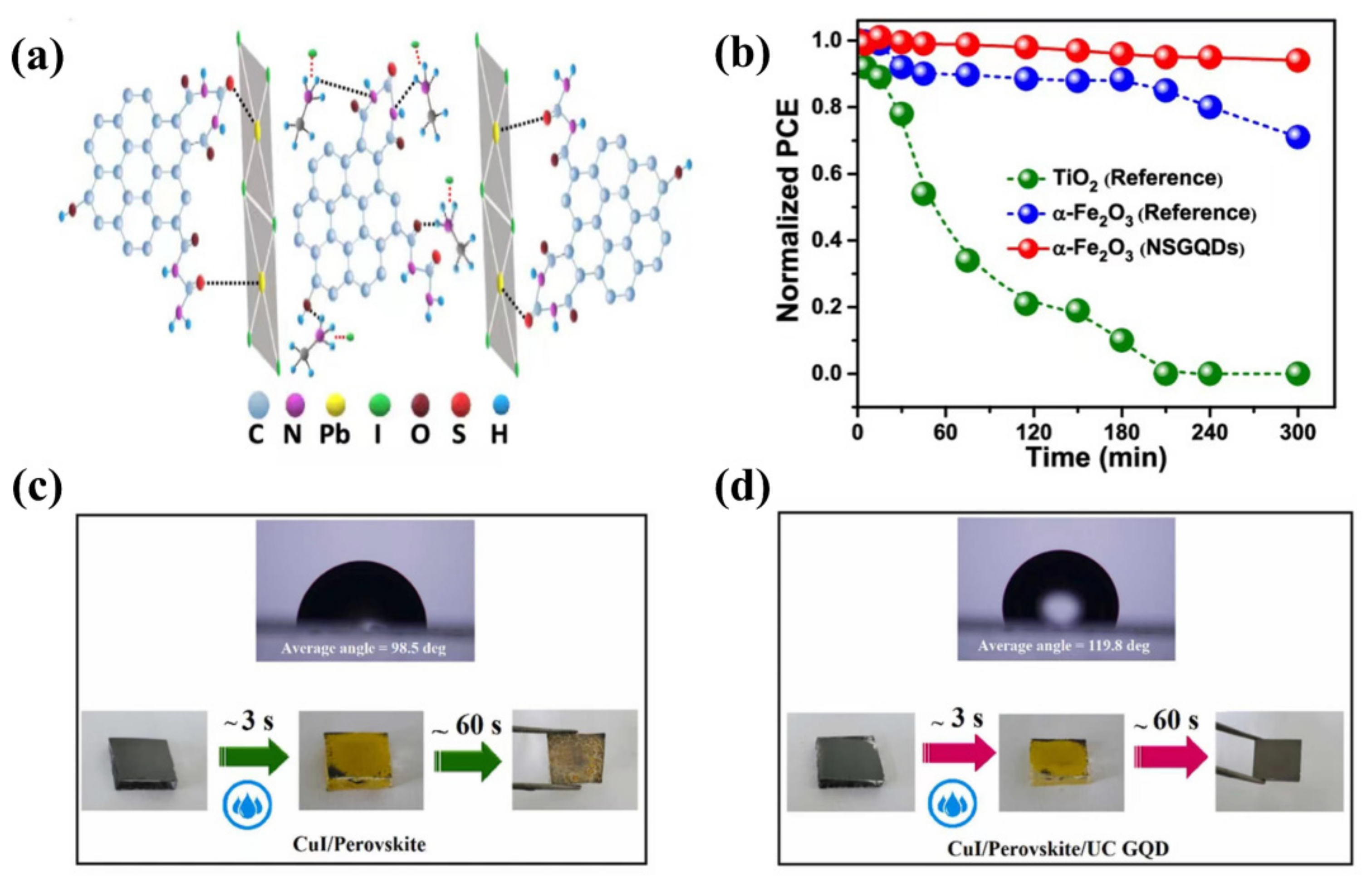
| NSGQDS | ~3 nm | FTO/α-Fe2O3/NSGQDs/ MAPbI3:NSGQDs/ NSGQDs/Spiro-OMeTAD/Au | 1.03 | 23.50 | 79 | 19.20 | [78] |
| I-GQDs | 10 nm | ITO/SnO2/I-GQDs/FAPbI3/ PCBM:C60/Ag | 1.073 | 25.42 | 82 | 22.37 | [79] |
| UC GQDs | 4~4.5 nm | FTO/CuI/ Cs0.05(MA0.17FA0.83)0.95Pb(I0.83Br0.17)3/ UC GQDs/PCBM/Au | 1.15 | 20.99 | 82 | 19.79 | [80] |
| Graphdiyne | 3~5 nm | FTO/TiO2/GD QDs/CH3NH3PbI3:GD QDS/Spiro-OMeTAD:GD QDs/Au | 1.12 | 22.48 | 79 | 19.89 | [83] |
| Graphite carbon nitride | 10~30 nm | FTO/SnO2/Graphite carbon nitride QDs/CsxMAyFA1−x−yPbIzBr3−z/ Spiro-OMeTAD/Au | 1.14 | 23.39 | 80 | 21.23 | [77] |
| QDs | Size | Device Structure | Voc | Jsc | FF % | PCE % | Ref. |
|---|---|---|---|---|---|---|---|
| CsPbI3 | ~10 nm | ITO/PTAA/ Cs0.05(FA0.83MA0.17)0.95Pb(I0.83Br0.17)3 /CsPbI3 QDs/C60/BCP/Cu | 1.15 | 22.90 | 78 | 20.60 | [86] |
| CsPbBr3 | ~18 nm | ITO/PTAA/ Cs0.05(FA0.83MA0.17)0.95Pb(I0.83Br0.17)3 /CsPbBr3 QDs/C60/BCP/Cu | 1.19 | 22.95 | 77 | 21.03 | [85] |
| CsPbBrCl2 | ~7 nm | ITO/PTAA/MAPbI3/CsPbBrCl2 QDs/ C60/BCP/Copper | 1.15 | 23.40 | 80 | 21.5 | [84] |
| QDs | Size | Device Structure | Voc | Jsc | FF % | PCE % | Ref. |
|---|---|---|---|---|---|---|---|
| PbS | 5 nm | FTO/TiO2/PbS QDs/CH3NH3PbI3/P3HT/Pt | 0.88 | 6.30 | 49.3 | 4.92 | [87] |
| CdS | 4~5 nm | ITO/m-TiO2/CdS QDs/MAPbI3/ Spiro-OMeTAD/Au | 0.94 | 16.86 | 64 | 10.52 | [93] |
| CdS | 5 nm | FTO/c-TiO2/CdS QDs/MAPbI3/ Spiro-OMeTAD/Au | 0.95 | 20.6 | 54 | 13.2 | [94] |
| CdSe | 2.4~3.5 nm | ITO/c-TiO2/m-TiO2/CdSe QDs/MAPbI3/ Spiro-OMeTAD/Au | 1.08 | 20.57 | 70 | 15.68 | [99] |
| CdSe@ZnS | 6~7 nm | ITO/PEDOT:PSS/MAPbI3/CdSe@ZnS QDs/C60/BCP/Ag | 1.08 | 23.5 | 77 | 19.6 | [95] |
| CuInS2 | 3~5 nm | ITO/TiO2 nanorod arrays/CuInS2 QDs/ MAPbI3/Spiro-OMeTAD/Au | 0.98 | 17.60 | 69 | 11.70 | [96] |
| CuInS2 | 1~3 nm | FTO/TiO2/CuInS2 QDs/MAPbI3/ Spiro-OMeTAD/Au | 0.98 | 19.2 | 71 | 13.3 | [97] |
| NaYF4:Yb/Er | 16.3 nm | FTO/c-TiO2/NaYF4:Yb/Er QDs/CH3NH3PbI3/ Spiro-OMeTAD/Ag | 1.06 | 23.1 | 73.8 | 18.1 | [98] |
| QDs | Size | Device Structure | Voc | Jsc | FF % | PCE % | Ref. |
|---|---|---|---|---|---|---|---|
| CQDs | ~20 nm | FTO/c-TiO2/m-TiO2/ CsPbBr3/CQDs/ Spiro-OMeTAD/Ag | 1.06 | 11.34 | 69 | 8.29 | [100] |
| E-g-C3N4 | 20~50 nm | FTO/c-TiO2/CH3NH3PbI3/E-g-C3N4 QDs/Spiro-OMeTAD/Au | 1.10 | 23.2 | 62 | 15.8 | [101] |
| Hydrophobic GQDs | 7 nm | ITO/SnO2/CH3NH3PbI3/HGQDs/ Spiro-OMeTAD/Au | 1.10 | 22.27 | 75 | 18.30 | [102] |
| QDs | Size | Device Structure | Voc | Jsc | FF % | PCE % | Ref. |
|---|---|---|---|---|---|---|---|
| CsPbBrI2 | 15~20 nm | FTO/TiO2/CsPbBrI2/CsPbBrI2 NSs/CsPbBrI2 QDs/PTAA/Au | 1.19 | 12.93 | 80.5 | 12.39 | [108] |
| CsPbBrI2 | 10~15 nm | FTO/c-TiO2/CsPbBrI2/ CsPbBrI2 QDs/PTAA/Au | 1.22 | 14.51 | 79.6 | 14.12 | [112] |
| CsPbBr3 | ~7.5 nm | ITO/SnO2/MAPbI3/CsPbBr3 QDs/Spiro-OMeTAD/Au | 1.11 | 23.57 | 76.88 | 20.17 | [111] |
| CsPbI3 | 9~13 nm | FTO/c-TiO2/m-TiO2/ MA0.17FA0.83Pb(I0.83Br0.17)3/ CsPbI3 QDs/Spiro-OMeTAD/Au | 1.09 | 24.42 | 69.72 | 18.56 | [105] |
| Mn-CsPbI3 | 15~20 nm | FTO/c-TiO2/CsPbI2Br/Mn-CsPbI3 QDs/PTAA/Au | 1.20 | 14.45 | 78.7 | 14.45 | [104] |
| Cs0.57FA0.43PbI3 | 10.7 nm | FTO/SnO2/FAPbI3/Cs0.57FA0.43PbI3 QDs/Spiro-OMeTAD/Au | 1.12 | 24.44 | 76 | 20.82 | [110] |
| CsPbBr1.85I1.15 | ~10 nm | FTO/c-TiO2/m-TiO2/ Cs0.05(FA0.85MA0.15)0.95Pb(I0.85Br0.15)3/CsPbBr1.85I1.15 QDs/ Spiro-OMeTAD/Au | 1.14 | 23.42 | 79 | 21.14 | [109] |
| MAPbBr0.9I2.1 | ~5 nm | FTO/c-TiO2/MAPbI3/ MAPbBr0.9I2.1 QDs/ Spiro-OMeTAD/Cr/Au | 0.95 | 19.51 | 72 | 13.32 | [103] |
Publisher’s Note: MDPI stays neutral with regard to jurisdictional claims in published maps and institutional affiliations. |
© 2022 by the authors. Licensee MDPI, Basel, Switzerland. This article is an open access article distributed under the terms and conditions of the Creative Commons Attribution (CC BY) license (https://creativecommons.org/licenses/by/4.0/).
Share and Cite
Zhou, Y.; Luo, X.; Yang, J.; Qiu, Q.; Xie, T.; Liang, T. Application of Quantum Dot Interface Modification Layer in Perovskite Solar Cells: Progress and Perspectives. Nanomaterials 2022, 12, 2102. https://doi.org/10.3390/nano12122102
Zhou Y, Luo X, Yang J, Qiu Q, Xie T, Liang T. Application of Quantum Dot Interface Modification Layer in Perovskite Solar Cells: Progress and Perspectives. Nanomaterials. 2022; 12(12):2102. https://doi.org/10.3390/nano12122102
Chicago/Turabian StyleZhou, Yankai, Xingrui Luo, Jiayan Yang, Qingqing Qiu, Tengfeng Xie, and Tongxiang Liang. 2022. "Application of Quantum Dot Interface Modification Layer in Perovskite Solar Cells: Progress and Perspectives" Nanomaterials 12, no. 12: 2102. https://doi.org/10.3390/nano12122102
APA StyleZhou, Y., Luo, X., Yang, J., Qiu, Q., Xie, T., & Liang, T. (2022). Application of Quantum Dot Interface Modification Layer in Perovskite Solar Cells: Progress and Perspectives. Nanomaterials, 12(12), 2102. https://doi.org/10.3390/nano12122102