Article

Transformation of Amorphous Terbium Metal–Organic Framework on Terbium Oxide TbOx(111) Thin Film on Pt(111) Substrate: Structure of TbxOy Film

1
Institute of Materials Research, Slovak Academy of Sciences, Watsonova 47, 040 01 Kosice, Slovakia
2
Institute of Catalysis, Bulgarian Academy of Sciences, Acad. G. Bonchev St., 1113 Sofia, Bulgaria
*
Author to whom correspondence should be addressed.
Nanomaterials 2022, 12(16), 2817; https://doi.org/10.3390/nano12162817
Submission received: 31 July 2022 / Revised: 10 August 2022 / Accepted: 14 August 2022 / Published: 17 August 2022
(This article belongs to the Special Issue Advanced Metal-Organic Frameworks)

Abstract

:
The present study is focused on the synthesis and structural properties of amorphous terbium metal–organic framework thin film (TbMOF-TF) and its transformation to terbium oxide by pyrolysis at 450 °C in the air. The crystalline (cTbMOF) and amorphous (aTbMOF) films were prepared by solvothermal synthesis using different amounts (0.4 and 0.7 mmol) of the modulator (sodium acetate), respectively. The powders were characterized by differential scanning calorimetry (DSC), thermogravimetry (TG), Fourier transform infrared (FTIR), Raman spectroscopy, and scanning electron microscopy (SEM). The varied chemical composition of the surface of TbMOFs and TbxOy was investigated by X-ray photoelectron spectroscopy (XPS). X-ray diffraction (XRD) and transmission electron microscopy (TEM) revealed that aTbMOF had been fully transformed to a Tb4O7 phase with a cubic crystal structure at 450 °C. The amorphous aTbMOF-TF film was prepared by dropping a colloidal solution of amorphous precursor nanocrystals on the SiO2/Si substrates covered with Pt as an interlayer. XPS confirmed the presence of Tb in two states, Tb3+ and Tb4+. The amorphous film has a rough, porous microstructure and is composed of large clusters of worm-like particles, while terbium oxide film consists of fine crystallites of cubic fluorite cF-TbOx, c-Tb4O7, and c-Tb2O3 phases. The surface topography was investigated by a combination of confocal (CM) and atomic force microscopy (AFM). The amorphous film is porous and rough, which is contrast to the crystalline terbium oxide film.

Graphical Abstract

1. Introduction

Metal–organic frameworks (MOFs), which belong to the subclass of porous coordination polymers (PCPs), are materials built from metal ions and organic bridging ligands [1,2]. MOFs have attracted much attention in various fields where they are used, such as sensor technology, catalysis, drug delivery, thin films, luminescence, gas storage, and separation [1].
Amorphous materials are excellent due to their “dangling bonds” and, in many applications, are more active than their crystalline counterparts [3,4,5,6]. While most research efforts have focused on crystalline MOFs, only a few amorphous (aMOFs) have been reported. From the study of Bennett et al. [7], it can be concluded that aMOFs created by introducing pressure, temperature, or ball milling still preserve the basic building blocks and short-range connectivity. FeMOF has a nanocomposite structure containing both crystalline and amorphous phases [8]. Lanthanide metal–organic frameworks (LnMOFs) are currently gaining increasing attention due to their potential applications in areas such as gas adsorption, catalysis, magnetism, and especially for their photoluminescence properties [9,10].
Nowadays, MOFs are available in several structures, such as nanocrystals (NCs), nanospheres, nanosheets, needles, hierarchical monoliths, thin films (TFs), membranes, and glasses [11]. Amongst these structures, MOF-TFs have attracted more attention due to their great potential in the development of nanotechnology applications such as optics, photonics, electronics, catalytic coatings, solar cells, batteries, and supercapacitors [11]. MOF-TFs deposited on substrates of variant functions have various applications [11,12]. In terms of fabrication techniques, commonly used procedures are known, such as hydro/solvothermal synthesis, layer-by-layer (LBL), and electrochemical methods. The coordination modulation method was first described by Kitagawa and Ferey for the synthesis of MOF nanocrystals [13,14]. Cai et al. and Li et al. later adopted this method to synthesize LnMOF nanocrystals using some monocarboxylic acids and carboxylate salts as modulators [10,15]. In special conditions, when redundant amounts of the modulator are added, the synthesis can lead to the origin of amorphous aMOF-TF [16]. Crystalline TbMOF as Tb(BTC)(H2O), prepared by the solvothermal synthesis, with the addition of 1,3,5-benzene tricarboxylic acid (BTC) and sodium acetate (NaOAc), changed when the amount of NaOAc was increased up to 0.7 mmol, resulting in the formation of the product in the amorphous phase [10].
Terbium oxides are used in various scientific and technological applications, such as optical, ceramic, and chemical ones [17]. The conventional thermolysis of Tb salts in the air usually yields oxygen-deficient fluorite terbium oxides TbOx of type x ≈ 1.75 [17]. These oxides were—by mistake—considered to be single-phase intermediate Tb4O7, but in fact, such a crystalline phase cannot be obtained, and the oxides TbO1.75 appeared to be two-phase mixtures of the related fluorite trigonal Tb7O12 and triclinic Tb11O20 [17,18]. Porous bimetallic Ce1−xTbxOy crystals in powder form were prepared by the direct pyrolysis of Ce1−xTbx-MOFs precursors [19]. It is known that in binary Tb oxides, the cations can exist in two states: Tb3+ and Tb4+ [17]. These distinct Tb3+/Tb4+ cation equilibria lead to different phase transitions, such as Tb02, Tb11O20, Tb4O7, and Tb7O12 [20]. Terbium oxides include the stoichiometric oxides Tb2O3 and TbO2, as well as non-stoichiometric oxides TbO1.714, TbO1.750, TbO1.818, TbO1.833, and TbO1.875 [21]. Non-stoichiometric oxides are transition compounds of hybrid efficiency with compositions ranging between Tb2O3 and TbO2. The highest terbium oxides (Tb11O20 and Tb7O12) are unstable and are subject to decomposition at high temperatures with the removal of oxygen. Tb11O20 converts to Tb7012 at ~600 °C in air and Tb7O12 to Tb2O3 above 1000 °C [21].
In films, all lanthanides can create stable sesquioxides (Ln2O3); only Pr and Tb are known to can form a wide range of intermediate oxides of Ln3+ and Ln4+ states (e.g., Pr6O11, Tb4O7) [22]. Terbium oxide films possess a wide variety of functional properties and can be used as gas sensors, luminophores, and optical electronics [23,24]. Polycrystalline terbium oxide films were grown on Si(111) substrates by Tb(dpm)3 vapor decomposition [23,24]. After annealing in air at temperatures of 400 and 650 °C, the films of Tb11O20, Tb7O12, and Tb4O7 differed in composition [23,24]. Lee et al. [25,26] prepared terbium oxide films with varying thicknesses by reactive physical vapor deposition (RPVD) of metallic terbium on Pt(111) substrate. Hexagonal film growth proceeds according to the Stranski–Krastanov mechanism, in which oxygen-deficient cubic fluorite cF-TbOx(111) initially forms a well-connected wetting layer, and the phases of δ-Tb11O20, ι-Tb7O12, TbOx (x = 1.75), and cF-TbO3 are progressively formed [26]. Similarly, terbium oxide films prepared by RPVD deposition on Cu(111) contained crystalline hexagonal dendrites of cF-TbOx(111) [22].
In this work, we investigated the structural and morphological properties of amorphous TbMOF (powder and film) and its thermal decomposition to terbium oxide during pyrolysis at 450 °C. The TbMOF-TF thin film was prepared by solvothermal synthesis with a [Tb(btc)] structure (BTC: Benzene-1,3,5-tricarboxylate) on a Pt/SiO2/Si substrate. The chemical composition, microstructure, and topography of the TbMOF-TF and TbxOy-TF films were analyzed by XRD, FTIR, Raman spectra, SEM, TEM, AFM, and CM methods. We reported a facile strategy to prepare amorphous aMOFs by the introduction of Tb and further pyrolysis at 450 °C to form a unique terbium oxide thin film with a thickness of ~400 nm on a Pt/SiO2/Si substrate. The novelty is a fabricated porous film, which is composed of morphologically different phases TbOx, Tb4O7, and Tb2O3 nanoparticles. The prepared films are suitable candidates for optoelectronic applications as gas sensors.

2. Materials and Methods

2.1. Chemicals and Materials Used

All the chemicals used (including solvents) were of analytical grade, purchased from Sigma-Aldrich, and used as-is without any further purification. 1,3,5-benzenetricarboxylic acid (BTC), Tb(NO3)3·6H2O, N,N-dimethylformamide (DMF), sodium acetate (NaOAc), ethanol (EtOH), and deionized water were used for the solvothermal synthesis of the two MOF types, both crystalline (cTbMOF) and amorphous (aTbMOF).

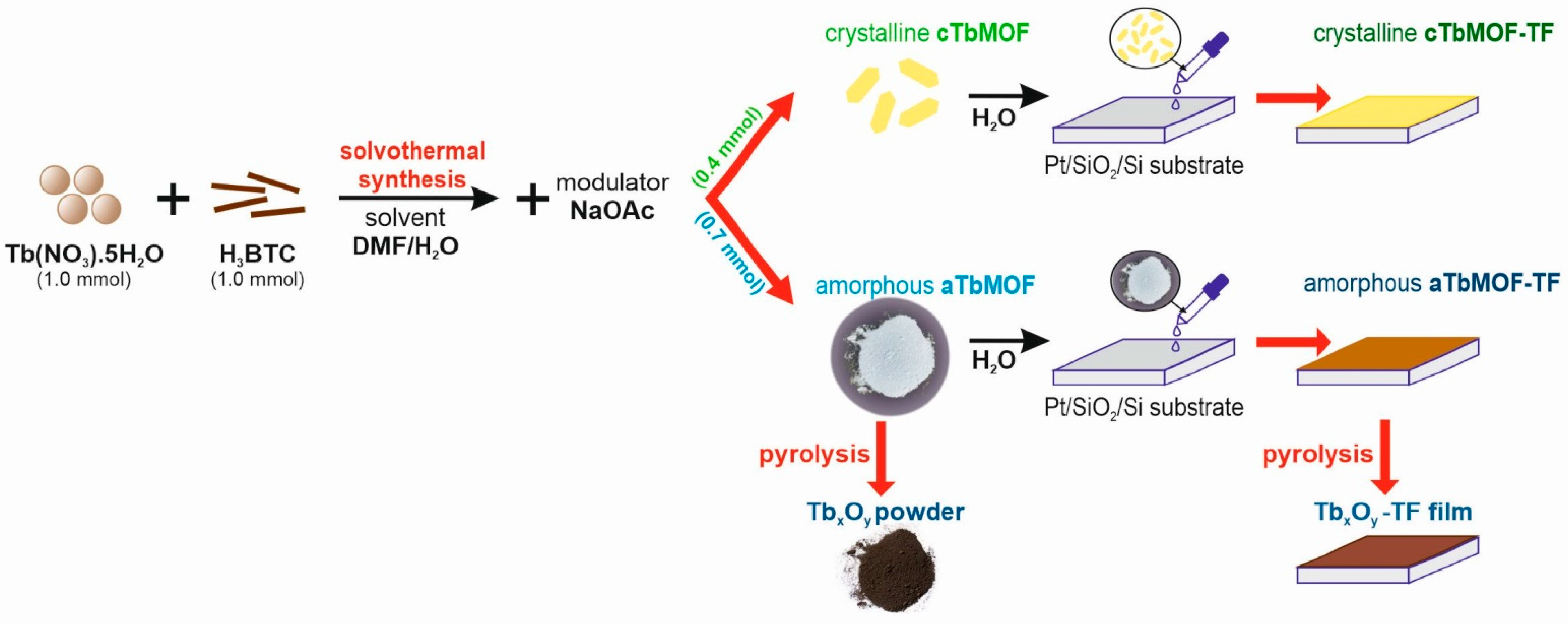
2.2. Preparation of cTbMOF and aTbMOF

The TbMOFs were prepared through modified solvothermal synthesis [7,10,19] according to previous work [27,28], as described in Scheme 1. Terbium(III) nitrate hydrate Ln(NO3)3·6H2O (1.0 mmol, 0.45 g) and H3BTC (1.0 mmol, 0.21 g) were dissolved in 30 mL of the DMF/H2O (1:1 v/v) solvents mixture together with the NaOAc modulator. The preparation procedures for cTbMOF and aTbMOF were the same and were performed using different amounts of modulator NaOAc for crystalline (0.4 mmol, 0.033 g) and amorphous (0.7 mmol, 0.055 g) TbMOFs. The two solutions of cTbMOF and aTbMOF were mixed at 25 °C for 1 h and then heated up to 60 °C, held for 48 h, and cooled down to room temperature. After synthesis, the products were isolated by centrifugation and washed several times with ethanol and water, respectively, and then dried in air. The prepared cTbMOF and aTbMOF had a yield of 70% (0.339 g) and 72% (0.349 g), respectively, without elemental analysis. The TbxOy crystals were prepared by calcination of the as-synthesized aTbMOF at 450 °C in the air for 2 h. The framework of the Ce1−xTbxMOF crystals was prepared using a similar method and started to collapse at 350 °C [19].

2.3. Preparation of cTbMOF-TF and aTbMOF-TF Thin Films

With the aid of crystalline and amorphous TbBTC colloidal seeds, the cTbMOF-TF and aTbMOF-TF thin films were prepared based on the substrates (Pt/SiO2/Si) at conditions similar to those described in Scheme 1. The powders of cTbMOF and aTbMOF were individually redispersed in H2O, so milky colloidal solutions were obtained with the concentrations of TbBTC of 0.03 g/mL. The colloidal solutions of the TbMOF were deposited onto the substrates by drop-casting. The mixed slurries were deposited on pre-cleaned silicon substrates covered with SiO2 and Pt. As the initial substrates, p-type silicon [100] single-crystal wafers with a diameter of 50 mm and 270 μm were used. The Pt layer was applied to the substrate by ion-sputtering from a Pt metal target. The final thickness of the Pt layer obtained on the surface of the 250 nm SiO2 film was about 20 nm. Continuous thin films of TbMOF were directly grown on Pt(111) [25,26]. MOFs were grown by repeating two drop-casting deposition cycles. The thickness of the MOF films can be easily controlled by the TbBTC concentration in the colloidal solution. The deposited films were then dried at 60 °C for 2 h. The prepared crystalline and amorphous TbBTC films were denoted as cTbMOF-TF and aTbMOF-TF. The TbxOy-TF thin film was prepared by calcination of the aTbMOF-TF thin film at 450 °C in the air for 2 h.

2.4. Characterization of the Obtained Powders (TbMOF and TbxOy) and Thin Films (TbMOF-TF and TbxOy-TF)

The thermal properties and the decomposition process of TbMOFs were analyzed by differential scanning calorimetry (DSC) coupled with thermogravimetric (TG) analysis (JUPITER STA 449-F1, NETZSCH, Selb, Germany) in platinum crucibles, temperature range of 50 to 1000 °C, and 10 °C min−1 heating rate in air. The chemical/phase composition of the obtained samples was studied by FTIR (Shimadzu (Kyoto, Japan) IRAffinity 1 with KBr pellets) and Raman spectroscopy (Raman spectroscope HORIBA BX 41TF, Kyoto, Japan); the phase composition was determined by X-ray diffraction analysis (XRD, X Pert Pro, Philips, Amsterdam, Netherlands, with CuKα radiation). The diffraction patterns were recorded in a 2θ range from 10 to 60° with a 4°min−1 scan rate. The additional composition and valence state inquiry was assessed by X-ray photoelectron spectroscopy (XPS). XPS measurements were carried out on an ESCALAB MkII (Thermo Fisher Scientific, Waltham, MA, USA) electron spectrometer equipped with a twin-anode MgKα/AlKα non-monochromated X-ray source. The measurements were taken with an AlKα X-ray source (1486.6 eV). The energy range was scaled using a standardizing C 1s line of acquired hydrocarbons to 285.0 eV for the electrostatic sample charging. The obtained data were analyzed and processed by SpecsLab2 CasaXPS 2.3.25 software (Casa Software Ltd., Berlin, Germany). The processing of the recorded spectra included a subtraction of X-ray satellites and Shirley-type background. The relative concentrations of the different chemical species were determined based on the normalization of the peak areas to their photoionization cross-sections, calculated by Scofield.
The surface morphologies of the samples were examined using Scanning Electron Microscopy (FESEM/FIB, Auriga Compact, Carl Zeiss, Oberkochen, Germany) equipped with an energy-dispersive X-ray analyzer (EDS) and high-resolution transmission electron microscopy (TEM, JEOL-JEM 2100F, Tokyo, Japan), using a scanning transmission electron microscopy mode (STEM) and EDS (Oxford Energy TEM250, Abingdon, UK). Before scanning, all samples were coated with carbon to enhance their conductivity. The surface topography and roughness of the films were estimated by a combination of confocal (CM, PluNeox 3D optical surface profiler by SENSOFAR (Barcelona, Spain) with 20× objective) and atomic force microscopy (AFM, Dimension ICON, by Veeco Instruments, Plainview, NY, USA).

3. Results and Discussion

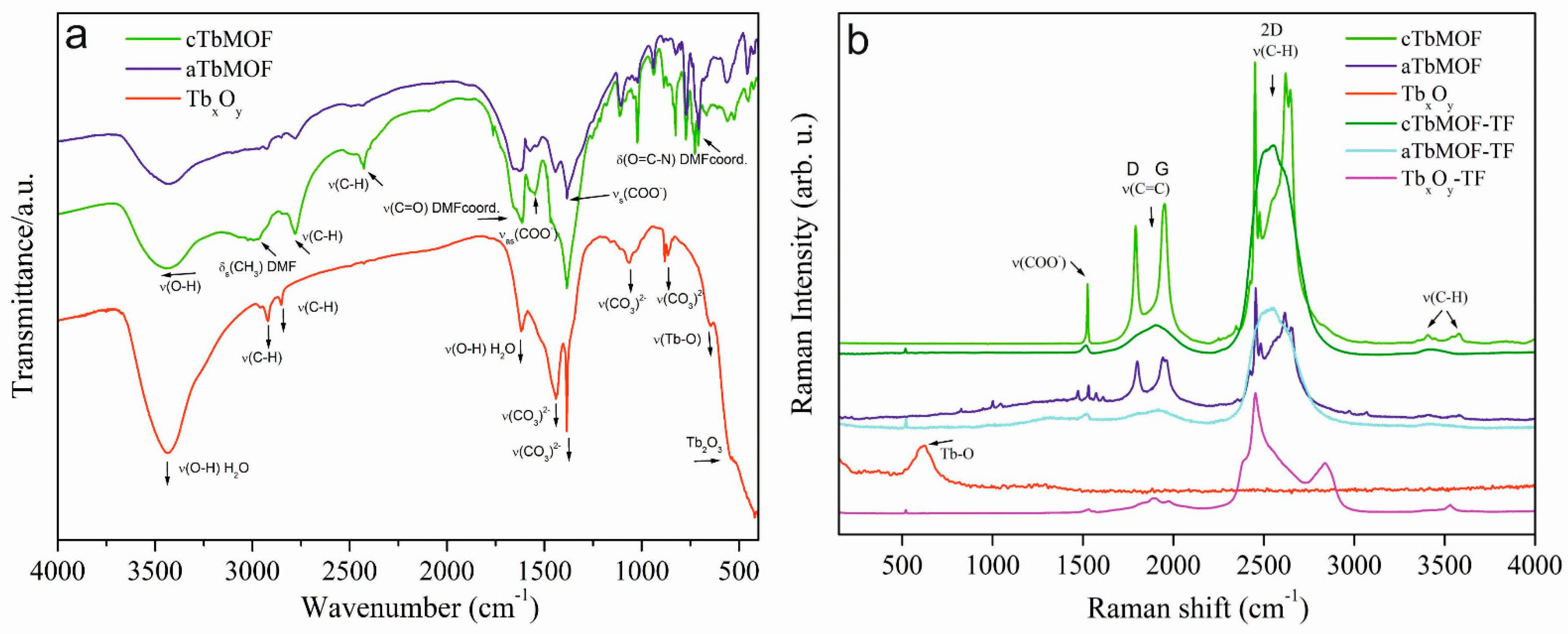
3.1. Structural Characterization of Tb-Based Powders and Thin Films

DSC and TG curves of crystalline cTbMOF, amorphous aTbMOF, and TbxOy powders are shown in Figure S1. Both samples of MOF have similar curves up to 400 °C. The weight losses in the temperature ranges of 150–220 °C and 220–350 °C are cognates with the release of trapped DMF solvent and water [29]. The notable difference between crystalline and amorphous MOF appears in the range of 410–650 °C. In this temperature region, the weight loss originates from the decomposition of the organic linkers of the framework. Amorphous MOF decomposes slowly by forming CO2 with an onset at ~380 °C and ending at ~650 °C, whereas crystalline start to release CO2 at higher temperatures of ~400 °C and up to ~670 °C. The TbMOFs have great thermal stability. After complete dehydration of terbium oxide (TbxOy sample) in the temperature range of ~50–200 °C, the carbonate structure of Tb2(CO3)3 was formed, which was thermally stable until 400 °C, after which it completely decomposed into terbium oxide Tb4O7 (wide exo peak at 700 °C) in the temperature range between 450 and 760 °C [30,31]. A small endo peak at 840 °C represents the transformation of Tb4O7 to Tb2O3 oxide [18]. Based on the DSC and TG results, it was confirmed that the amorphous aTbMOF was thermally decomposed into terbium oxide at 450 °C.
Figure 1 shows the FTIR and Raman spectra of amorphous (aTbMOF), crystalline (cTbMOF), and aTbMOF pyrolyzed at 450 °C (sample TbxOy) powders and corresponding films (TF). In the FTIR spectra (Figure 1a), the wide peak at 3435 cm−1 is assigned to υ (O–H) groups. The effect of acetate groups from sodium acetate for cTbMOF and aTbMOF can be noticed in the regions at 2998, 2780, and 2430 cm−1, which are assigned to stretching υ(C–H) vibrations. The peak at 1630 cm−1 belongs to ν(C=O) of DMF. In the spectra, the bands in zones 1560–1518 cm−1 and 1385 cm−1 were marked as stretching vibrations of the COO groups υas and υs, respectively. The powerful peaks provide the C–H bending benzene vibrations that shifted to the region of 765 and 720 cm−1 [28]. The peak that appeared at 565 cm−1 can be assigned to the stretching vibration of Tb–O. The structural designation of the TbMOFs is marked as [Tb(btc)(H2O)(dmf)] [27,28]. The peaks in the 1630–1370 cm−1 region disappear in the TbxOy sample, indicating that the TbMOF skeleton structure collapsed [19]. From FTIR analysis, we can see that crystalline TbxOy is a carbonate structure of Tb2(CO3)3·nH2O [32]. The bands located at 1440, 1380, 1060, and 876 cm−1 can be assigned to the carbonate (CO3)2− structure [21,32], whereas the bands at 3440 and 1615 cm−1 are assigned to the ν(O–H) and ν(HOH) modes of vibration of crystalline water, respectively [21].
The Raman spectra of powders and films are depicted in Figure 1b. The spectra of crystalline and amorphous samples of the same chemical composition can be significantly different, primarily because of the presence or absence of spatial order. Exceptional peaks at about 1795; 1950; and in the region of 2350–2800 cm−1, corresponding to D, G, and 2D bands, respectively, are also visible on the spectra. The peaks of the powders are sharper than those of the films. The development of the cTbMOF was confirmed by the detection of Raman bands at 1525, 1895, and 2540 cm−1, which were identified as ν(COO), ν(C=O), and ν(C–H), respectively, according to the literature [3]. The lines in the region of 2800–3100 cm−1 are ascribed to the stretching of the –CH group and asymmetric stretching of -NH bonds. Raman spectra of the films have broadened peaks. The peak at 520 cm−1 corresponds to the characteristic band of Tb–O [3,33]. Terbium oxide Tb4O7 has been reported as a mixed-valence compound with a non-stoichiometric structure [34]. The TbxOy powder shows one broadened peak at 620 cm−1. In the TbxOy-TF film, both the intensities of D and G peaks increase [23]. Raman spectra show that the carbonization and TbxOy-TF formation temperature is >400 °C. In agreement with the XRD, the FTIR spectra (Figure 1a and Figure 2a) for annealed aTbMOF sample also represent the remaining unchanged main building block of the MOF structure. The band recorded at 530 cm−1 assigned to the Tb–O bond [35] and sharp bands at 2485, 2845 cm−1, and 3523 cm−1 are (C–H) vibrations. In the FTIR and Raman spectra results, the bands consequent from the presence of ligands in aTbMOF were deleted, which is a qualitative confirmation of terbium oxide formation from a carbonate structure.
The crystalline cTbMOF complex is 3D open framework, and each asymmetric unit contains one eight-coordinated Tb3+ ion, one BTC ligand (C9H3O6), two coordinated DMF molecules (C3H7NO), and one free guest water molecule (H2O) [36,37] as Tb(BTC)(DMF)2·H2O. In Figure S2, each Tb3+ ion is coordinated with eight oxygen atoms from four BTC ligands through two chelating bidentate carboxylate groups, two monodentate carboxylate groups, and two terminal DMF molecules. The empirical formula is C15H19N2O9Tb [36].
Figure 2 shows the XRD patterns for both samples (crystalline and amorphous): TbMOF powders as-synthesized and after thermal treatment at 450 °C (TbxOy) of the same film. For cTbMOF, the results were compared with the crystallographic data in the Cambridge Database: CIF no. 617492 for Tb(BTC)(DMF)2·H2O; the match confirms the expected tetragonal phase for TbBTC [38]. As displayed in Figure 2a, all peaks of the sample synthesized with 0.4 mmol sodium acetate agree with the CIF, indicating they are phase Tb(BTC)(DMF)2·(H2O). When the amount of sodium acetate is increased to 0.7 mmol, an amorphous phase occurs [10,29]. For this sample, there is only one broad “hump” caused by diffuse scattering. This is a typical characteristic of amorphous aMOFs [5,9]. In XRD of TbxOy powder (Figure 2a), the peaks at 450 °C at 29.52, 33.9°, 48.6°, and 57.8° 2θ correspond to the (111), (200), (202), and (311) planes of Tb4O7 (PDF no. 13-0387). This indicates that after pyrolysis, the aTbMOF and cTbMOF precursor have been fully transformed into Tb4O7 with a cubic crystal structure [19,39]. Figure 2b shows the XRD pattern for cTbMOF-TF, aTbMOF-TF, and TbxOy-TF thin films on Pt/SiO2/Si substrates. Similar to the XRD of crystalline powder, the cTbMOF-TF film (TbBTC phase) reveals peaks at 10.5, 11.5, 16.1, 21.3, and 29.3° (2θ) and Pt and Si peaks from the substrate. Another film is the amorphous aTbMOF-TF, which pyrolyzed to (TbxOy-TF) consisting of three phases, cubic fluorite cF-TbOx (x = 1.75), PDF no. 03-065-7172) [40]; cubic c-Tb4O7 (PDF no. 13-0387) [21,23,41,42,43]; and cubic c-Tb2O3 (PDF no. 19-1326) [32]. The XRD spectrum of TbxOy-TF suggests that the film has binary terbium oxides with Tb4+ and Tb3+ states. The pyrolysis of TbMOF or Tb salts in the air generally yields oxygen-deficient, fluorite-related terbium oxides TbOx with a composition of x ≈ 1.75–1.83 [17]. Intermediate Tb11O20, Tb24O44, and Tb48O88 phases in the terbium oxide TbOx system have a fluorite structure [40]. Two oxides with the composition of Tb11O20 and Tb7O12 are probably formed at a temperature below 400 °C [23]. The TbO1.75 oxide appeared to represent a two-phase mixture of the fluorite-related stable ι-Tb11O20 (triclinic structure) and metastable δ-Tb7O12 (rhombohedral structure) [17]. The Tb7O12 phase is transformed to c-Tb4O7 and Tb2O3 at a temperature above 400 °C with corresponding mixtures of +3 and +4 valences [20,44]. Based on the XRD results, characteristic peaks of terbium oxide correspond with the crystalline structure of c-Tb4O7 in the TbxOy precursor and three phases (cF-TbOx, c-Tb4O7, and c-Tb2O3) in the TbxOy-TF film, and we did not observe the characteristic peaks of aTbMOF.

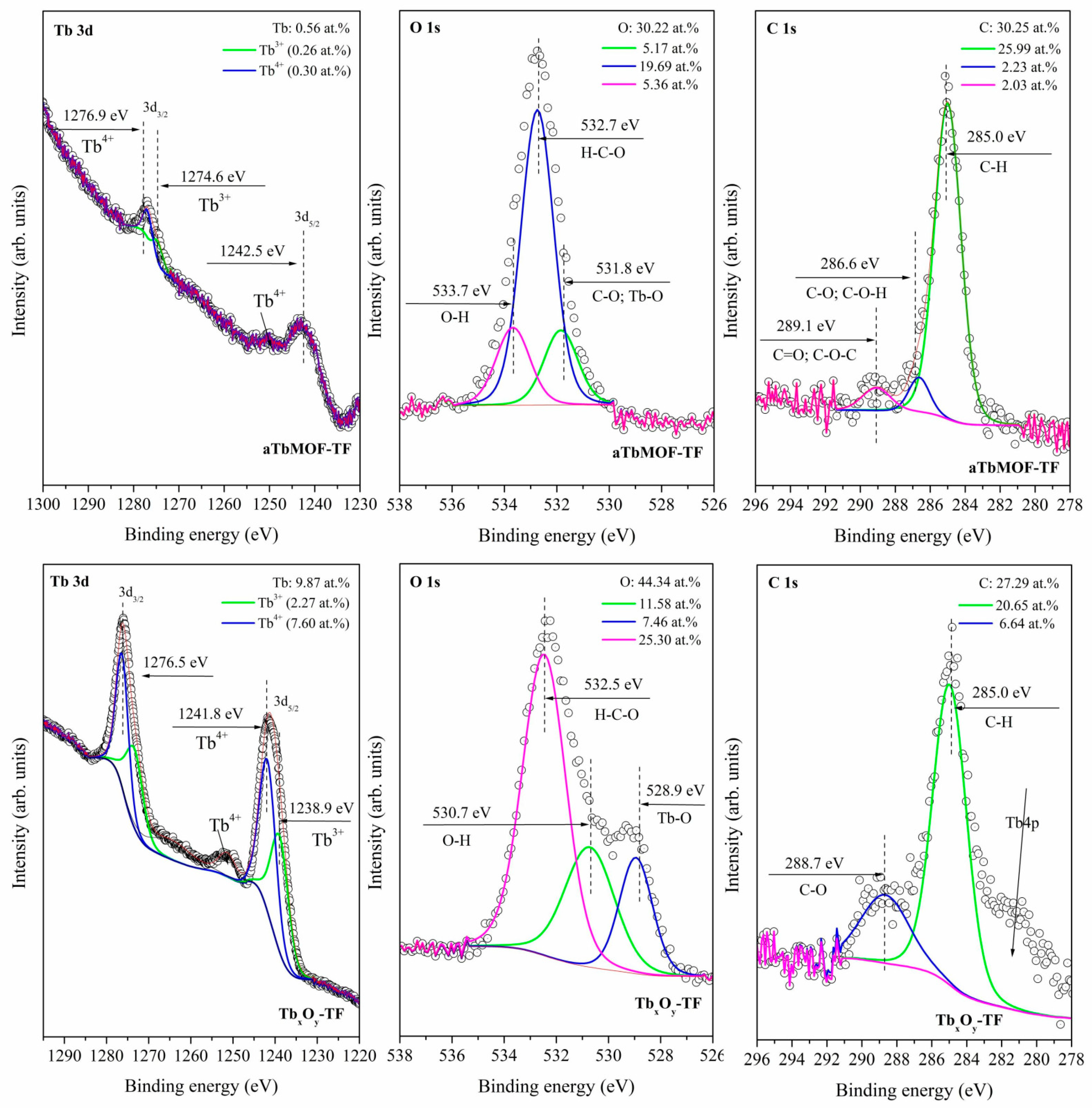
3.2. XPS Characterization of the Surfaces of Powders and Films

The XPS survey spectra for aTbMOF powder and aTbMOF-TF and TbxOy-TF films are shown in Figure S3, where all peaks corresponding to the characteristic electronic transitions of Tb, O, N and C and Pt and Si (from the substrate) for films are visible. The TbxOy-TF film contains carbon impurities. Tb 3d peak overlaps with the Auger peak of CKLL, and Tb 4d overlaps with Si 2s.
XPS core level spectra of Tb 3d, O 1s and C 1s for three samples are observed in Figure S4. The highest peaks for Tb 3d and Tb 4d are in TbxOy-TF film. The XPS Tb 3d spectrum for the samples represents two peaks at 1245 and 1277 eV, assigned to 3d5/2 and 3d3/2 of Tb3+, respectively. The presence of Tb4+ was found in a small peak at 1250 eV [28]. The XPS spectrum of O 1s and C 1s in all of the samples showed peaks centered at 533 and 285 eV, respectively. The total concentration in atomic percent of Tb, O, C and N elements on the surface of amorphous powder and both films was determined in Table S1.
XPS core-level spectra of Tb 3d, O 1s, and C 1s for aTbMOF-TF and TbxOy-TF films are depicted in Figure 3. The content of Tb, O, and C elements on the surface of the aTbMOF-TF film in at.% was determined as 0.56, 30.22, and 30.25 %, respectively. In TbxOy-TF film, the Tb and O content increases to 9.87 and 44.34%, respectively, but the C content decreases to 27.29%. The high-resolution (HR) XPS spectrum of the aTbMOF-TF film shows two peaks centered at 1276.9 (3d3/2) and 1242.5 eV (3d5/2), similar to TbxOy-TF film (1276.5 and 1241.8 eV).
Figure 3 shows the detailed Tb 3d core-level XPS spectra together with the deconvolution analysis of the various Tb valence states for both films. Since the Tb content in the MOF film is low (0.56 at. %), the intensity of both peaks (Tb 3d5/2 and Tb 3d3/2) is quite low, and the Tb 3d5/2 (1242.5 eV) peak overlaps with the Auger peak of CKLL; therefore, the analysis can only be realized over the Tb 3d3/2 peak. The Tb 3d5/2 band can be resolved into the two sub-bands peaking at 1274.6 (Tb3+) and 1276.9 eV (Tb4+). In the terbium oxide film (Tb 9.87 at.%), there are two principal Tb 3d5/2 and Tb 3d3/2 bands peaking at 1241.8 and 1276.5 eV, respectively. Two sub-bands peaking at 1238.9 and 1273.7 eV can be ascribed to the Tb3+ state, and the two peaking at 1241.8 and 1276.5 eV can be ascribed to the Tb4+ state. According to XPS analysis results, Zhu et al. [42] reported Tb2O3 (Tb3+) and TbO2 (Tb4+) in the Tb4O7 film.
The O 1s peak was deconvoluted, and three peaks centered at 531.8, 532.7, and 533.7 eV were attributed to the Tb–C–O, H–C–O, and O–H, bonds of aTbMOF-TF. The binding energy of O 1s changes from its initial 528.9 eV (Tb–O) via 530.7 (O–H) to 532.5 eV (H–C–O) in the TbxOy-TF film. In the aTbMOF-TF film, the C 1s peak was deconvoluted into peaks centered at 285.0, 286.6, and 289.1 eV, representing C–H, C–O, C–O–H, and C=O/C–O–C, respectively. In the TbxOy-TF film, the peak at 285.0 eV is related to C-H bonds. The peak at 288.7 eV is related to C-O bonds as carbonates (CO3)2−. The XPS C 1s, O 1s, and Tb 3d core level spectra of amorphous film and its annealed sample are supported well by the XRD, Raman, and FTIR results. Qualitatively appreciable change is detected for the sample annealed up to 450 °C, with clear framework decomposition (mainly in the form of CO2 loss) and carbonization [35].
Figure S5 shows the Pt 4f spectra of the Pt/SiO2 substrate in aTbMOF-TF film. It is the Pt 4f (4f7/2 and 4f5/2) doublet signal from the spectrum at 71.1 and 74.5 eV, respectively. The binding energy (Pt 4f7/2) for the sample was 71.1 eV, which is the same as the corresponding value of 71.2 eV for bulk platinum metal (Pt0) [45]. After annealing of the film at 450 °C (TbxOy-TF), the Pt 4f signal shifted by 0.2 eV to a lower BEs (Figure S6). Figure S5 shows the XPS Si 2s and Tb 4d core-level spectra recorded in the high-resolution mode at 149.9 (Si4+) and 149.9 eV (Tb3+). The XPS spectrum of the Si 2p line at 103.2 eV (Si4+, SiO2) in the TbxOy-TF sample is shown in Figure S6. In the Pt/SiO2/Si substrate, Pt 4f is about 0.5 eV higher BE in comparison to the samples with both films; therefore, we assume that we have some interaction between Pt and silicon substrate. A binding energy of 72.8 eV is typical for Pt/Si, Pt2Si, Pt(OH)2, and even for PtSi [45]. XPS confirmed the presence of Tb in two Tb3+ and Tb4+ valence states in both films.

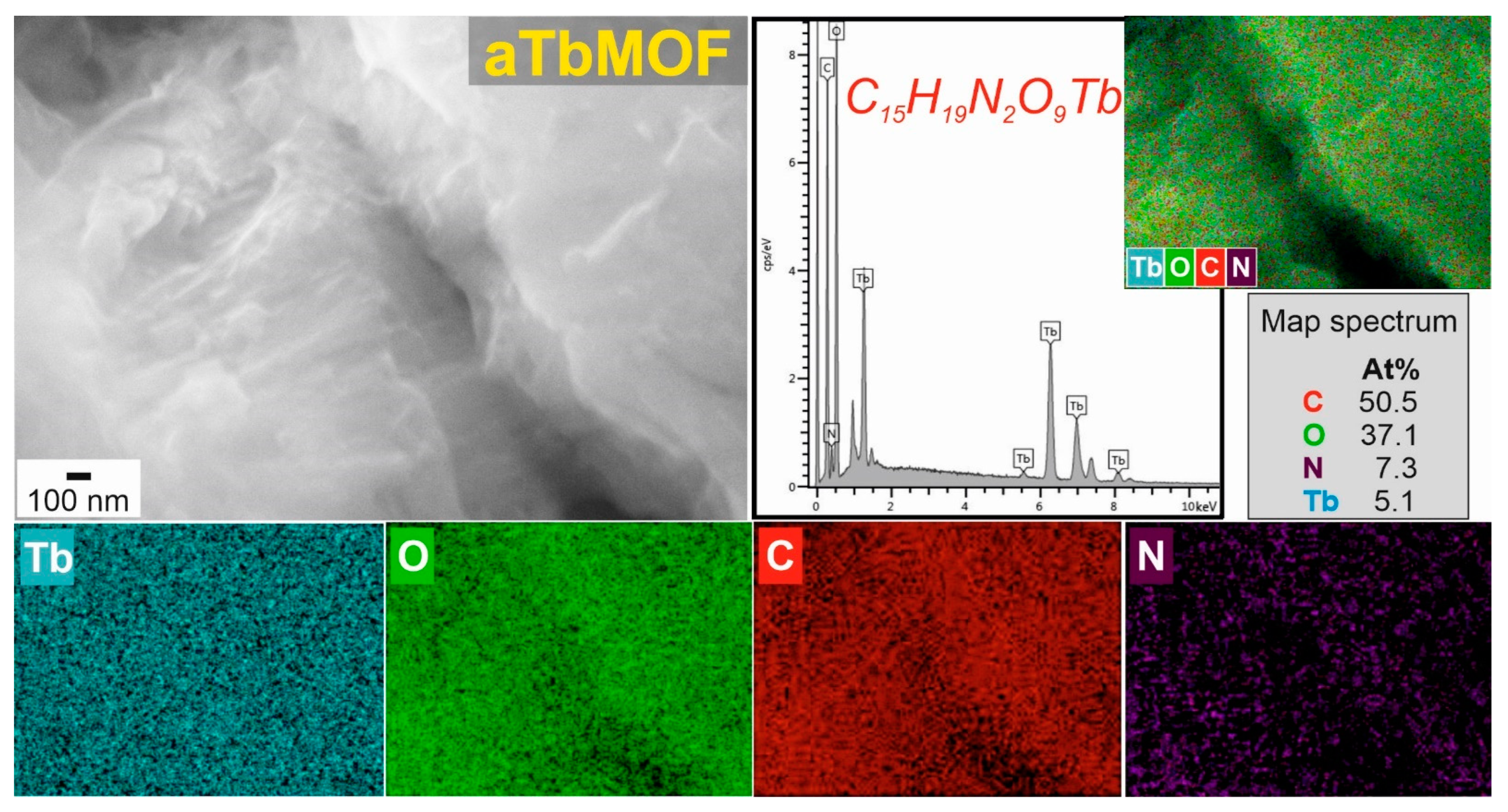
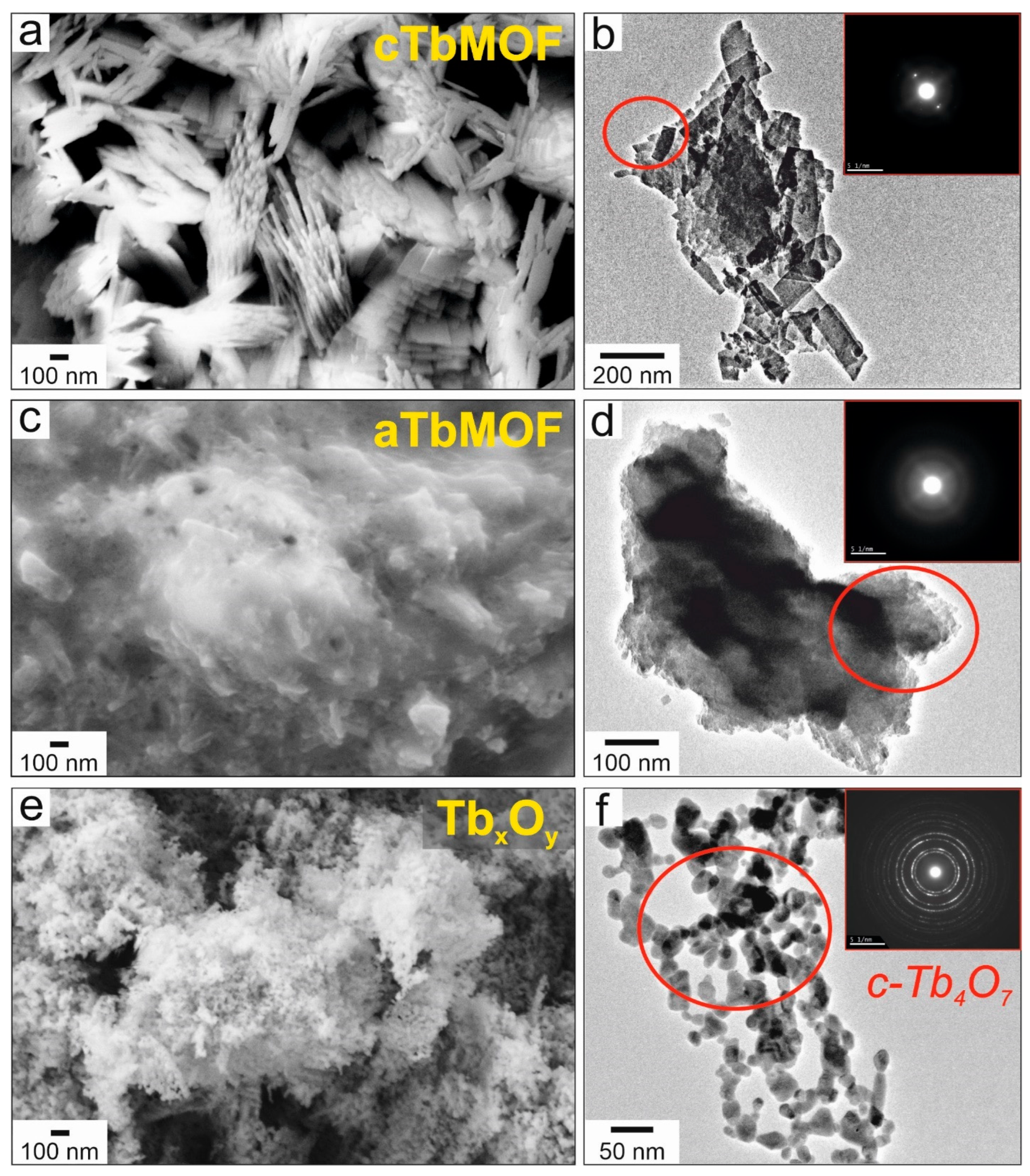
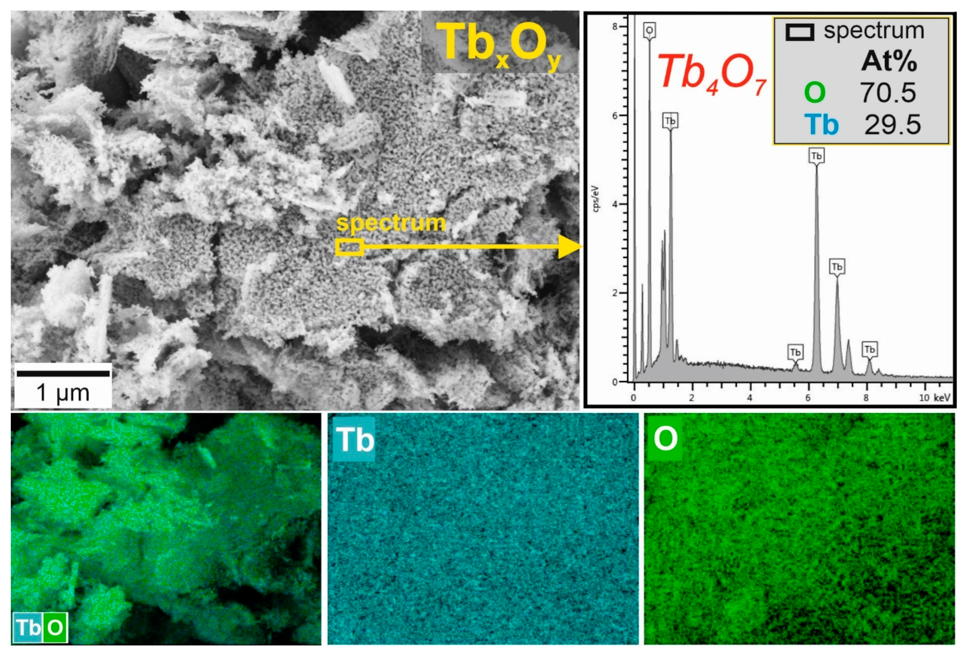
3.3. Morphological Characterization of Powders

The surface morphology of the samples was characterized using SEM and TEM. The images of TbMOF (crystalline and amorphous) and TbxOy powders are shown in Figure 4 and Figure S7. Observation of crystalline cTbMOF in Figure 4a reveals that the nano straw sheaves ~500 nm in length contained smaller rice-like crystals. As shown in Figure 4b, nanoparticles of TbBTC with an average size of 200 nm were observed by TEM, similar to particles of another lanthanide DyBTC with a NaOAc modulator [29]. Amorphous aTbMOF (confirmed by XRD analysis) was obtained when the amount of NaOAc was 0.7 mmol (Figure 4c,d and Figure S7a,b). The high-resolution transmission electron microscopy (HR-TEM) image reveals no lattice fringes, and the selected area electron diffraction (SAED) shows no perceptible diffraction rings (Figure 4d and Figure S7b). Figure 4e and Figure S7c depict the SEM surface morphology of the pyrolyzed aTbMOF sample. This TbxOy powder exhibits a sponge-like surface. In addition, the surface of samples is covered with randomly distributed pores [21]. During annealing, uniform nanoparticles of Tb oxide are formed and aggregated to Tb4O7 crystals (Ostwald ripening) [19]. The TEM images of the TbxOy powder (Figure 4f and Figure S7d) show that the particles of Tb4O7 were irregular in shape. The aggregates are composed of small primary nanoparticles (10–20 nm). This range of sizes is in agreement with the size (6–12 nm) for Tb4O7 reported in the literature [21].
The SEM images and EDS mapping (Figure 5 and Figure 6) of aTbMOF and TbxOy samples further detected the presence of Tb, O, and C as incorporated elements in the amorphous sample and Tb4O7, respectively. EDS spectra of aTbMOF and TbxOy show significant peaks of elements in surface samples. The surface composition for aTbMOF in at.% of Tb, O, C, and N were determined as 5.1, 37.1, 50.5, and 7.3, respectively. The values calculated for the assumed formula of crystalline [Ln(btc)(dmf)2(H2O)], C15H19N2O9Tb is C9.9HxN1.4O7.3Tb. The concentration of the Tb and O elements (in at.%) from the EDS spectra of the TbxOy sample are 29.5 and 79.5, respectively. It is known that in binary Tb oxides, the terbium cations can exist in two states: Tb3+ and Tb4+ [17]. These various Tb3+/Tb4+ cationic equilibria lead to different phase transitions, such as TbO2, Tb11O20, Tb4O7, and Tb7O12 [20].
Clusters of small nanoparticles of Tb4O7 (TEM images) are shown in Figure 7. Terbium oxide prepared from aTbMOF by pyrolysis at 450 °C (sample TbxOy) has a fine crystalline structure with crystallite sizes ranging from 5 to 20 nm, as seen in Figure 7a,b. From the results of the selected area, electron diffraction (SAED) (Figure 7c) determined a cubic c-Tb4O7 structure with a space group of F m-3m (225) [17,43]. The HR TEM image (Figure 7b) showed that the lattice spacings of the nanoparticles were 0.31 and 0.273 nm, close to the values of the interplanar distance of the (111) and (200) planes for the Tb4O7 nanostructure. Specifically, the average background subtraction filtering (ABSF) image (Figure 7d) indicated an interplanar spacing of 0.308 nm for the (111) plane, 0.271 nm for the (200) plane, and 0.192 nm for the (200) plane of the cubic Tb4O7. These observations are in agreement with XRD (Figure 2a) and the EDS spectrum in Figure 7e. SEM and TEM results of powders showed the clusters of small Tb4O7 nanoparticles with various morphologies and irregular shapes with crystallite sizes ranging from 5 to 20 nm in comparison with straw sheaves ~500 nm in length for crystalline cTbMOF and an amorphous morphology of aTbMOF.

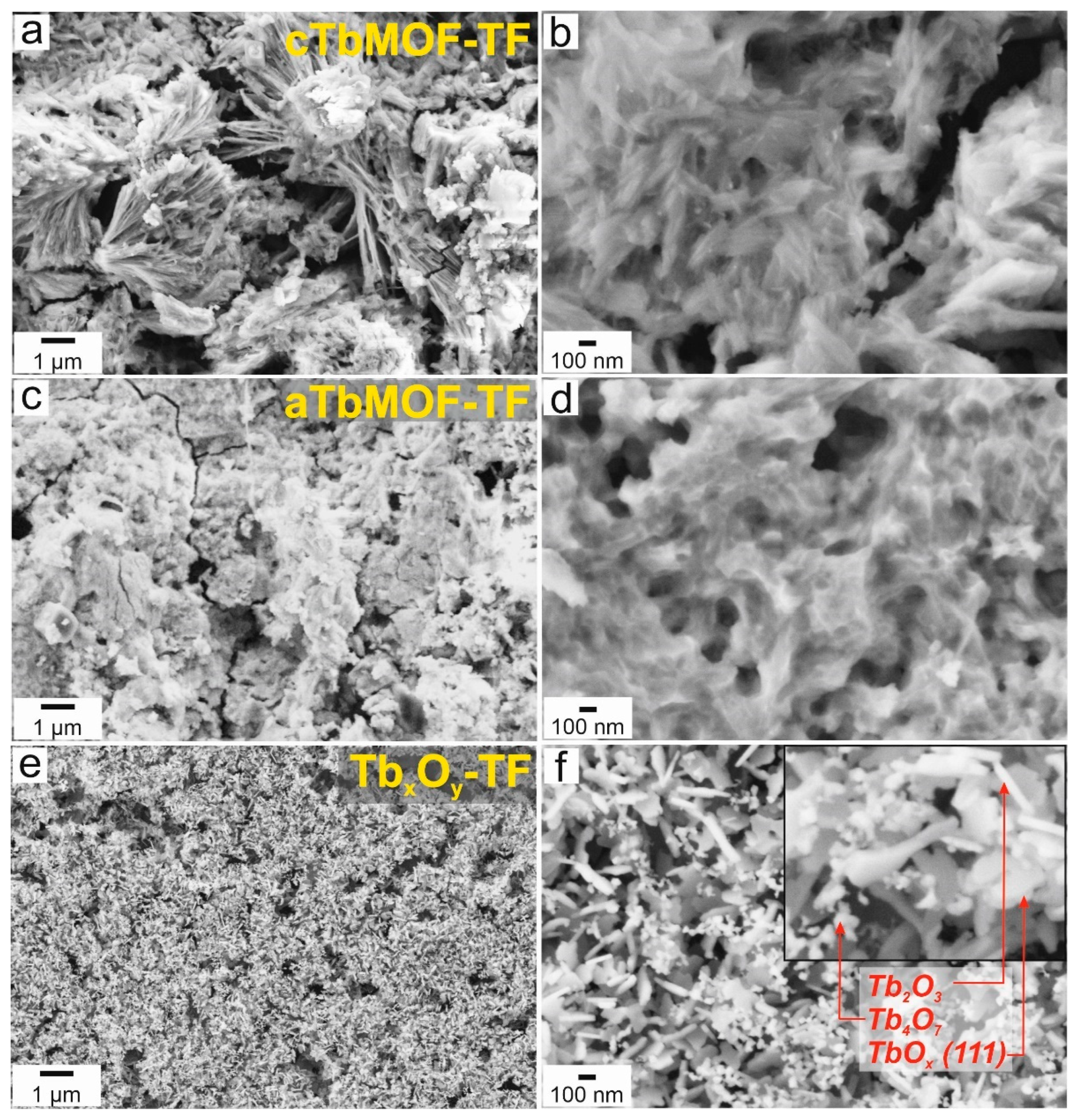
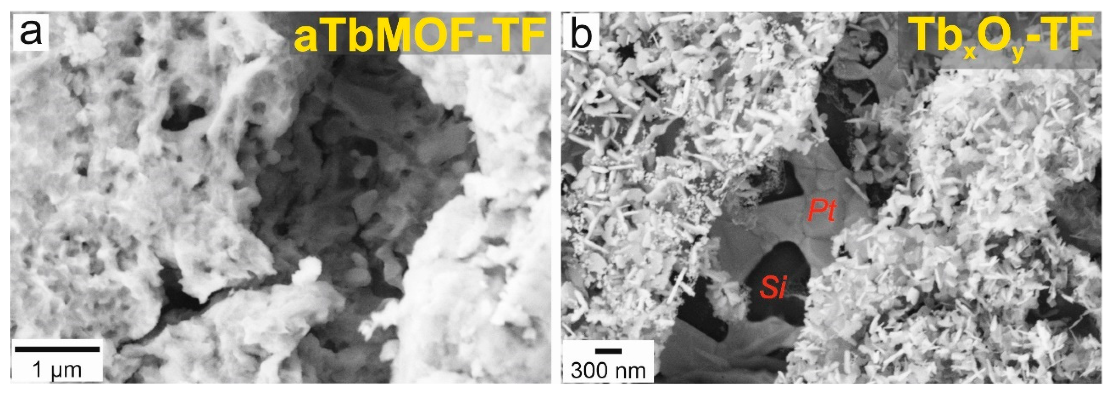
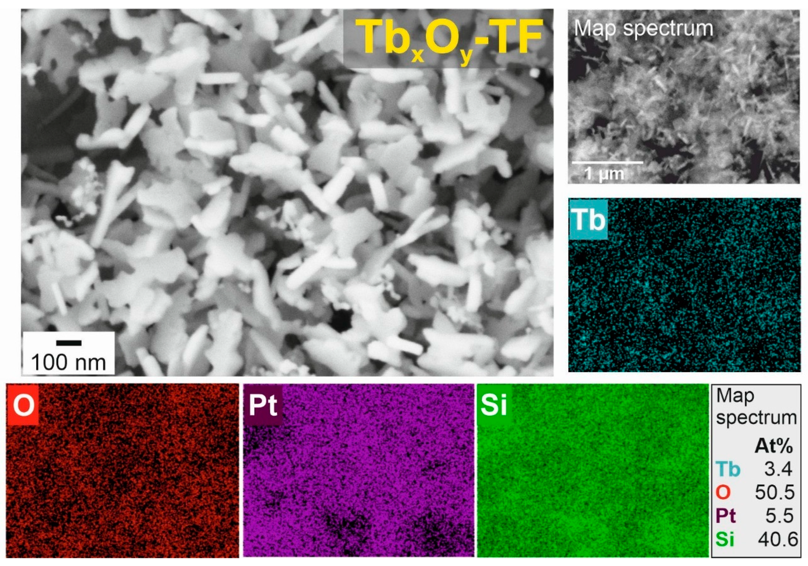
3.4. Morphological Characterization of Films

SEM surface microstructures of TbMOF (crystalline and amorphous) and terbium oxide films prepared on Pt/SiO2/Si are shown in Figure 8. The SEM image of cTbMOF (Figure 8a,b) reveals a straw sheaf-like structure, which is in agreement with that reported in the literature [46]. As shown in Figure 8b, the MOF needle-like particles display different elongated shapes 80–150 nm in size in the porous microstructure of the crystalline film. A SEM image of amorphous MOF film shows that the surface of samples becomes very rough (Figure 8c,d). A similar microstructure with a very rough amorphous MOF surface was observed in aNiFeMOF and aFeCoMOF with worm-like particles [3,6]. SEM image clearly shows the macroporous structure of aMOF, which is formed by worm-like nanoparticles with a diameter of ~100 nm (Figure 8d). In Figure 8e,f we see the macroporous surface microstructures of the amorphous TbMOF film annealed at 450 °C (TbxOy-TF sample). A mixture of three terbium oxide structures with different shapes: TbOx (flower-like), Tb4O7 (flakes), and Tb2O3 (needles), according to XRD data (Figure 4b), is recorded in the enlarged SEM image (Figure 8f). For comparison, the SEM surfaces of microstructures of the Pt layer on SiO2/Si substrates deposited and annealed at 450 °C are observed in Figure S8a,b, respectively. The Pt/SiO2/Si substrate secures Pt(111) as nucleation sites and improves the growth of aTbMOF film on its surface (Figure 9a), along with the adhesion between the TbxOy film and Pt layer (Figure 9b). The SiO2 layer (~250 nm) is visible below the Pt layer (~20 nm) of the substrate. The thickness of TbxOy and TbMOF films is ~400 nm and ~900 nm, respectively. Figure S9a visualizes the size of pores in the range of 73 to 180 nm for the amorphous MOF film. In Figure S9b, the particle shape and size of TbOx (flower-like, 119 nm), Tb2O3 (needles, 183 nm), and Tb4O7 (flakes, 38 nm) can be observed.
The polycrystalline terbium oxide film differed in composition and consisted of cubic fluorite cF-TbOx(111), cF-Tb2O3, and c-Tb4O7 phases [23,24]. The TbxOy-TF film grows by a mechanism that is analogous to the Stranski–Krastanov mechanism in that single wetting layer forms of TbOx (x = 1.75), followed by the growth of well-defined, multilayered islands [25,26,47]. Relatively strong interaction with the Pt(111) surface forces the TbOx thin film to adopt a defective fluorite structure rather than the preferred bixbyite (Tb2O3) structure [47]. Irregularly shaped TbOx islands coexist with smaller flower-like particles [22]. These are crystalline with hexagonal structures concerning the Pt(111) surface, which is consistent with cubic fluorite TbOx(111) [22]. The flower-like structure of TbOx consists of plentiful leaf-like nanolayers grown outwardly, which leads to a high surface area. These nanosheets are approximately 30 nm in thickness and 100 nm in width [48]. The formation of the c-Tb2O3(111) phase (needles) likely occurs through the successive formation of metastable orthorhombic ι-Tb7O12 and triclinic δ-Tb11O20 phases, which were consistent with c-Tb4O7 (flakes) and the variable-density TbOx phase [26].
In Figure S10 and Figure 10, the SEM and EDS mapping of the elements in the aTbMOF-TF and TbxOy-TF films are shown. EDS spectra of the films show several peaks corresponding to Tb, O, and C elements (Figure S10) and Tb and O (Figure 10), whereas Pt and Si are from the substrate, and the molar ratios of terbium ions matched well with the supposed compound formula. In SEM results, thermal decomposition of worm-like particles in the microstructure of the amorphous aTbMOF-TF film caused the formation of nanoparticles with three terbium oxide structures of different shapes and sizes.

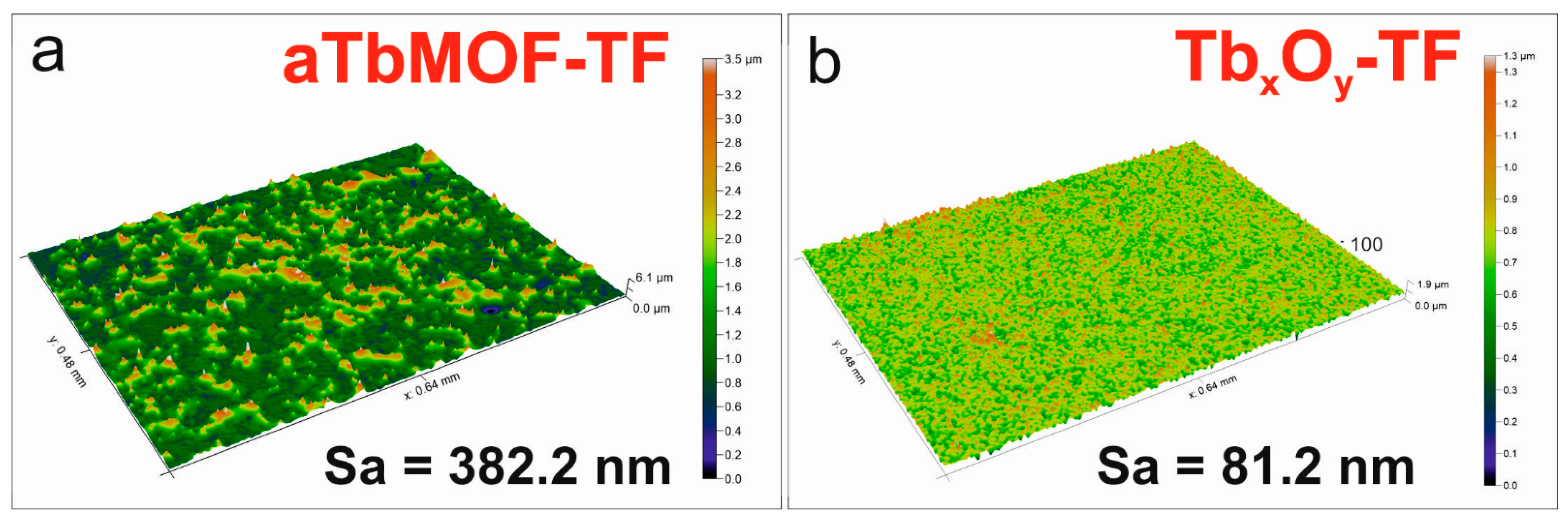
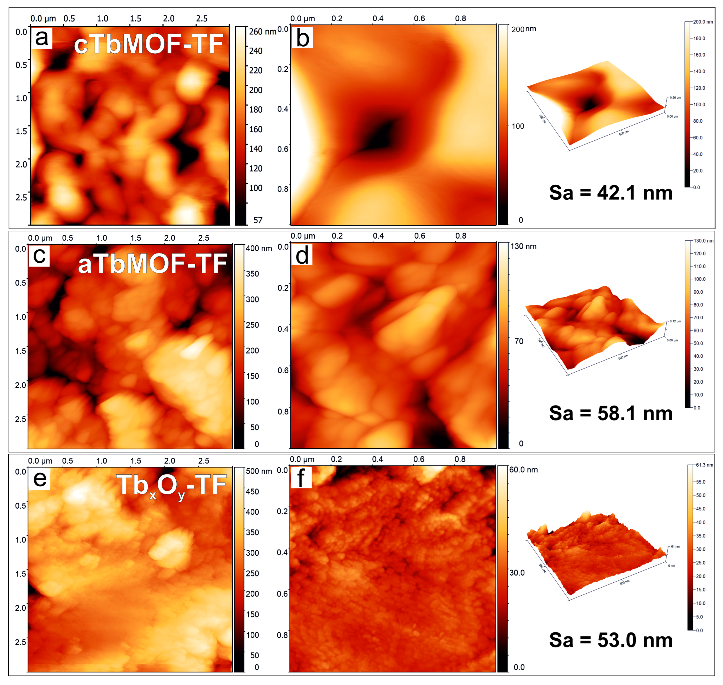
3.5. Topography Characterization of Films

The surface topography of the films was investigated by a combination of atomic force (AFM) and confocal microscopy (CM). After the Pt deposition on the SiO2/Si substrate, AFM and CM measurements were performed to confirm the coating uniformity and study the homogeneity of the Pt interlayer (Figure S11). AFM revealed the particulate nature of the coating and allowed us to determine the mean size of the particles, which was measured as about 20 nm. One can see the presence of areas with a low surface roughness of the Pt films, giving average roughness of Sa = 1.5 nm (AFM) according to 3 μm × 3 μm and 1 μm × 1 μm scans in Figure S11a,b and Sa = 5.9 nm (CM) by 0.68 mm × 0.48 mm (637 µm × 478 µm) (Figure S11c,d).
Figure 11 shows AFM images of porous TbMOF (crystalline and amorphous) and TbxOy-TF thin films. Two-dimensional and three-dimensional AFM images show that the cTbMOF-TF (Figure 11a,b) film surface topography consists of uniform clusters of particles. These areas disappear on the surface of the amorphous film (Figure 11c,d), and its roughness for the same size of scan is higher compared to crystalline MOF film [3,6]. The Pt film on the substrate formed a homogenous nanoparticulate layer, which acts as an intermediate one and improves the adhesion of the amorphous TbMOF-TF film to the substrate. Thermal treatment does not only lead to MOF structure elimination but also decreases the roughness of the TbxOy-TF film surface (Figure 11e,f). Sa surface roughness values of the films were calculated as 42.1 nm for cTbMOF-TF, 58.1 nm for aTbMOF-TF, and 53.0 nm for TbxOy-TF films from a 3 μm × 3 μm image. According to the roughness of Sa obtained from the CM results shown in Figure 12, the amorphous film (Figure 12a) is very rough and is composed of large clusters, which is contrast to terbium oxide film (Figure 12b).
The combination of the applied spectroscopic methods lets us conclude that we have taken an amorphous TbMOF thin film and subsequently transformed it into oxide film, which was shown to be of rather fine quality. The AFM and CM surface profile corresponds very well with the SEM micrographs of films depicted in Figure 8. Additionally, the SEM and XRD results of films show the formation of TbOx, Tb2O3, and Tb4O7 particles in the TbxOy-TF film.
Further investigations of samples of thin films can involve luminescence characterization as the terbium mean lifetime and quantum efficiency. TbMOF-TF and terbium oxide films have great application prospects in luminescence sensing, especially in biological and environmental luminescent sensors.

4. Conclusions

The crystalline and amorphous terbium metal–organic frameworks (TbMOFs) powders were prepared by solvothermal synthesis using different amounts of sodium acetate (NaOAc) as a modulator. A higher concentration of modulator may lead to the formation of amorphous aTbMOF. A porous amorphous aTbMOF-TF thin film was obtained by deposition from a water suspension of amorphous powder on the SiO2/Si substrates using Pt(111) as an interlayer. The amorphous MOF powder and corresponding amorphous film, after pyrolysis at 450 °C in the air, were transformed into terbium oxide TbxOy and TbxOy-TF, respectively. The TbxOy powder consists of a single cubic phase c-Tb4O7 and has a fine crystalline structure with crystallite sizes ranging from 5 to 20 nm, in contrast to the porous TbxOy-TF film, which is composed of three different phases, namely, cubic fluorite cF-TbOx(111); (x = 1.75), c-Tb4O7, and c-Tb2O3. The different morphologies and sizes of particles of flower-like TbOx (~119 nm) islands, needle-like Tb2O3 (~183 nm), and flake-like Tb4O7 (~38 nm) were observed. XPS established the presence of Tb in two valence states, Tb3+/Tb4+, in films.
Thermal treatment not only led to MOF structure transformation but also a reduction in average roughness (Sa) of the TbxOy-TF film surface. Sa surface roughness values, obtained by CM, were calculated as 382 nm for aTbMOF-TF and 81 nm for TbxOy-TF. The presented methodology is suitable for the preparation of terbium oxide films for optoelectronic and sensor applications.

Supplementary Materials

The following supporting information can be downloaded at: https://www.mdpi.com/article/10.3390/nano12162817/s1, Figure S1: DSC/TG curves of crystalline (cTbMOF), amorphous (aTbMOF), and amorphous aTbMOF powders, heated at 450 °C (TbxOy); Figure S2: Coordination environment of Tb(BTC)(DMF)2(H2O); TbMOF, Figure S3: XPS survey spectra of amorphous powder (aTbMOF), amorphous thin film (aTbMOF-TF), and TbxOy-TF on SiO2/Si substrates with Pt interlayer; Figure S4: HR XPS spectra of Tb 3d, O 1s, and C 1s for amorphous aTbMOF powder and aTbMOF-TF film and TbxOy-TF film; Figure S5: HR XPS spectra of Pt 4f and Si 2s and Tb 4d for amorphous aTbMOF-TF thin film; Figure S6: HR XPS spectra of Pt 4f and Si 2p (substrate) for TbxOy-TF thin film; Figure S7: SEM and TEM images of (a,b) amorphous aTbMOF and (c,d) TbxOy powders; Figure S9: SEM surface microstructures of (a) aTbMOF-TF (with pore sizes) and (b) TbxOy-TF thin films (with particle sizes); Figure S10: SEM surface microstructures and EDS elemental mapping of the amorphous aTbMOF-TF thin film; Figure S11: (a,b) 2D and 3D-AFM topography and (c,d) confocal microscopy (CM) scans of the Pt/SiO2/Si substrate sample in isometric and 3D representations of Pt-interlayer; Table S1: XPS elemental atomic % of aTbMOF, aTbMOF-TF, and TbxOy-TF samples.

Author Contributions

Investigation, conceptualization, resources, writing—original draft preparation, H.B.; writing—review and editing, methodology, H.B. and E.M.; investigation, formal analysis, M.S., L.M., T.S., I.S., A.K., M.L. and H.K. All authors have read and agreed to the published version of the manuscript.

Funding

The research was supported by the Grant Agency of the Slovak Academy of Sciences through project VEGA no. 2/0037/20 and APVV-20-0299.

Data Availability Statement

The data presented in this study are available on request from the corresponding author. These data are not publicly available due to excessive size and complex format.

Conflicts of Interest

The authors declare no conflict of interest.

References

  1. Nasruddin, N.; Zulys, A.; Fayza, Y.; Buhori, A.; Naufal, M.; Ghiyats, M.; Saha, B.B. Synthesis and characterization of a novel microporous lanthanide based metal-organic framework (MOF) using napthalenedicarboxylate acid. J. Mater. Res. Technol. 2020, 9, 7409–7417. [Google Scholar] [CrossRef]
  2. Zhong, M.; Kong, L.; Zhao, K.; Zhang, Y.H.; Li, N.; Bu, X.H. Recent Progress of Nanoscale Metal-Organic Frameworks in Synthesis and Battery Applications. Adv. Sci. 2021, 8, 2001980. [Google Scholar] [CrossRef] [PubMed]
  3. Wei, K.; Wang, X.; Jiao, X.; Li, C.; Chen, D. Self-supported three-dimensional macroporous amorphous NiFe bimetallic-organic frameworks for enhanced water oxidation. Appl. Surf. Sci. 2021, 550, 149323. [Google Scholar] [CrossRef]
  4. Fonseca, J.; Gong, T.; Jiao, L.; Jiang, H.L. Metal-organic frameworks (MOFs) beyond crystallinity: Amorphous MOFs, MOF liquids and MOF glasses. J. Mater. Chem. A 2021, 9, 10562. [Google Scholar] [CrossRef]
  5. Bennett, T.D.; Cheetham, A.K. Amorphous Metal-Organic Frameworks. Acc. Chem. Res. 2014, 47, 1555–1562. [Google Scholar] [CrossRef]
  6. Liu, C.; Wang, J.; Wan, J.; Cheng, Y.; Huang, R.; Zhang, C.; Hu, W.; Wei, G.; Yu, C. Amorphous Metal-Organic Framework-Dominated Nanocomposites with Both Compositional and Structural Heterogeneity for Oxygen Evolution. Angew. Chem. Int. Ed. 2019, 132, 14587. [Google Scholar] [CrossRef]
  7. Yang, F.; Li, W.; Tang, B. Facile Synthesis of Amorphous UiO-66 (Zr-MOF) for Supercapacitor Application. J. Alloys Compd. 2018, 733, 8–14. [Google Scholar] [CrossRef]
  8. Sapnik, A.F.; Bechis, I.; Collins, S.M.; Johnstone, D.N.; Divitini, G.; Smith, A.J.; Chater, P.A.; Addicoat, M.A.; Johnson, T.; Keen, D.A.; et al. Mixed hierarchical local structure in a disordered metal–organic framework. Nat. Commun. 2021, 12, 2062. [Google Scholar] [CrossRef]
  9. Colodrero, R.M.P.; Papathanasiou, K.E.; Stavgianoudaki, N.; Olivera-Pastor, P.; Losilla, E.R.; Aranda, M.A.G.; León-Reina, L.; Sanz, J.; Sobrados, I.; Choquesillo-Lazarte, D.; et al. Multifunctional Luminescent and Proton-Conducting Lanthanide Carboxyphosphonate Open-Framework Hybrids Exhibiting Crystalline-to-Amorphous-to-Crystalline Transformations. Chem. Mater. 2012, 24, 3780–3792. [Google Scholar] [CrossRef]
  10. Cai, D.; Guo, H.; Wen, L.; Liu, C. Fabrication of hierarchical architectures of Tb-MOF by a ‘‘green coordination modulation method’’ for the sensing of heavy metal ions. Cryst. Eng. Comm. 2013, 15, 6702–6708. [Google Scholar] [CrossRef]
  11. Zhang, Y.; Chang, C.H. Metal-Organic Framework Thin Films: Fabrication, Modification, and Patterning. Processes 2020, 8, 377. [Google Scholar] [CrossRef]
  12. Hu, M.; Shu, Y.; Kirillov, A.; Liu, W.; Yang, L.; Dou, W. Epoxy Functional Composites Based on Lanthanide Metal−Organic Frameworks for Luminescent Polymer Materials. ACS Appl. Mater. Interfaces 2021, 13, 7625–7634. [Google Scholar] [CrossRef]
  13. Tsuruoka, T.; Furukawa, S.; Takashima, Y.; Yoshida, K.; Isoda, S.; Kitagawa, S. Nanoporous nanorods fabricated by coordination modulation and oriented attachment growth. Angew. Chem. Int. Ed. 2009, 48, 4739–4743. [Google Scholar] [CrossRef] [PubMed]
  14. Horcajada, P.; Serre, C.; Grosso, D.; Boissière, C.; Perruchas, S.; Sanchez, C.; Férey, G. Colloidal Route for Preparing Optical Thin Films of Nanoporous Metal–Organic Frameworks. Adv. Mater. 2009, 21, 1931–1935. [Google Scholar] [CrossRef]
  15. Li, X.; Lu, S.; Tu, D.; Zheng, W.; Chen, X. Luminescent lanthanide metal-organic framework nanoprobes: From fundamentals to bioapplications. Nanoscale 2020, 12, 15021–15035. [Google Scholar] [CrossRef] [PubMed]
  16. Shan, B.; James, J.B.; Armstrong, M.R.; Close, E.C.; Letham, P.A.; Nikkhah, K.; Lin, Y.S.; Mu, B. Influences of Deprotonation and Modulation on Nucleation and Growth of UiO-66: Intergrowth and Orientation. J. Phys. Chem. C 2018, 122, 2200–2206. [Google Scholar] [CrossRef]
  17. Fursikov, P.V.; Abdusalyamova, M.N.; Makhmudov, F.A.; Shairmardanov, E.N.; Kovalev, I.D.; Kovalev, D.Y.; Morgunov, R.B.; Koplak, O.V.; Volodin, A.A.; Khodos, I.I.; et al. Structural features and magnetic behavior of nanocrystalline powders of terbium oxide prepared by the thermal decomposition of terbium acetate in air. J. Alloys Compd. 2016, 657, 163–173. [Google Scholar] [CrossRef]
  18. Balabanov, S.S.; Permin, D.A.; Rostokina, E.Y.; Egorov, S.V.; Sorokinb, A.A.; Kuznetsov, D.D. Synthesis and structural characterization of ultrafine terbium oxide powders. Ceram. Int. 2017, 43, 16569–16574. [Google Scholar] [CrossRef]
  19. Zhao, L.; Sun, K.; Youliwasi, N.; Guo, H.; Yang, G.; Jiao, F.; Dong, B.; Chai, Y.; Mintova, S.; Liu, C. Highly Sensitive H2O2 Sensor Based on Porous Bimetallic Oxide Ce1−xTbxOy Derived from Homeotypic Ln-MOFs. Appl. Surf. Sci. 2019, 470, 91–98. [Google Scholar] [CrossRef]
  20. Veber, P.; Velázquez, M.; Gadret, G.; Rytz, D.; Peltz, M.; Decourt, R. Flux growth at 1230 °C of cubic Tb2O3 single crystals and characterization of their optical and magnetic properties. Cryst. Eng. Comm. 2015, 17, 492–497. [Google Scholar] [CrossRef]
  21. Abu-Zied, B.M.; Mohamed, A.R.N.; Asiri, A.M. Effect of Thermal Treatment on the Formation, Textural and Electrical Conductivity Properties of Nanocrystalline Tb4O7. J. Nanosci. Nanotechnol. 2015, 15, 4487–4492. [Google Scholar] [CrossRef] [PubMed]
  22. Höcker, J.; Cartas, W.; Schaefer, A.; Bäumer, M.; Weaver, J.F.; Falta, J.; Flege, J.I. Growth, Structure, and Stability of the High-index TbOx(112) Surface on Cu(111). J. Phys. Chem. C 2015, 119, 14175–14184. [Google Scholar] [CrossRef]
  23. Belaya, S.V.; Bakovets, V.V.; Boronin, A.I.; Koshcheev, S.V.; Lobzareva, M.N.; Korolkov, I.V.; Stabnikov, P.A. Terbium oxide films grown by chemical vapor deposition from terbium(III) dipivaloylmethanate. Inorg. Mater. 2014, 50, 379–386. [Google Scholar] [CrossRef]
  24. Belaya, S.V.; Bakovets, V.V.; Asanov, I.P.; Korolkov, I.V.; Sulyaeva, V.S. MOCVD Synthesis of Terbium Oxide Films and their Optical Properties. Chem. Vap. Depos. 2015, 21, 150–155. [Google Scholar] [CrossRef]
  25. Lee, C.J.; Mehar, V.; Weaver, J.F. Growth and Structure of Tb2O3(111) Films on Pt(111). J. Phys. Chem. C 2018, 122, 9997–10005. [Google Scholar] [CrossRef]
  26. Lee, C.J.; Sayal, A.; Vashishtha, S.; Weaver, J.F. Redox-mediated transformation of a Tb2O3(111) thin film from the cubic fluorite to bixbyite structure. Phys. Chem. Chem. Phys. 2020, 22, 379–390. [Google Scholar] [CrossRef]
  27. Brunckova, H.; Mudra, E.; Rocha, L.; Nassar, E.; Nascimento, W.; Kolev, H.; Kovalcikova, A.; Molcanova, Z.; Podobova, M.; Medvecky, L. Preparation, and characterization of isostructural lanthanide Eu/Gd/Tb metal-organic framework thin film for luminescent applications. Appl. Surf. Sci. 2021, 542, 148731. [Google Scholar] [CrossRef]
  28. Brunckova, H.; Mudra, E.; Rocha, L.; Nassar, E.; Nascimento, W.; Kolev, H.; Lisnichuk, M.; Kovalcikova, A.; Molcanova, Z.; Streckova, M.; et al. Nanostructure and Luminescent Properties of Bimetallic Lanthanide Eu/Gd, Tb/Gd and Eu/Tb Coordination Polymers. Inorganics 2021, 9, 77. [Google Scholar] [CrossRef]
  29. Guo, H.; Zhu, Y.; Wang, S.; Su, S.; Zhou, L.; Zhang, H. Combining Coordination Modulation with Acid-Base Adjustment for the Control over Size of Metal-Organic Frameworks. Chem. Mater. 2012, 24, 444–450. [Google Scholar] [CrossRef]
  30. Utochnikova, V.V.; Pietraszkiewicz, O.; Kozbiał, M.; Gierycz, P.; Pietraszkiewicz, M.; Kuzmina, N.P. Mixed-ligand terbium terephthalates: Synthesis, photophysical and thermal properties and use for luminescent terbium terephthalate thin film deposition. J. Photochem. Photobiol. A Chem. 2013, 253, 72–80. [Google Scholar] [CrossRef]
  31. Siqueira, A.B.; Carvalho, C.T.; Ionashiro, E.Y.; Bannach, G.; Rodrigues, E.C.; Ionashiro, M. Synthesis, characterization and thermal behavior of solid 2-methoxybenzoates of trivalent metals. J. Therm. Anal. Calorim. 2008, 92, 945–951. [Google Scholar] [CrossRef]
  32. Rahimi-Nasrabadi, M.; Pourmortazavi, S.M.; Ganjali, M.R.; Norouzi, P. Nanosized terbium carbonate, and oxide particles: Optimized synthesis, and application as photodegradation catalyst. J. Mater. Sci. Mater Electron 2018, 29, 2988–2998. [Google Scholar] [CrossRef]
  33. Malasi, A.; Taz, H.; Farah, A.; Patel, M.; Lawrie, B.; Pooser, R.; Baddorf, A.; Duscher, G.; Kalyanaraman, R. Novel Iron-based ternary amorphous oxide semiconductor with very high transparency, electronic conductivity, and mobility. Sci. Rep. 2015, 5, 18157. [Google Scholar] [CrossRef] [PubMed]
  34. Cui, J.; Hope, G.A. Raman and Fluorescence Spectroscopy of CeO2, Er2O3, Nd2O3, Tm2O3, Yb2O3, La2O3, and Tb4O7. J. Spectrosc. 2015, 2015, 940172. [Google Scholar] [CrossRef]
  35. Gadipelli, S.; Guo, Z. Postsynthesis Annealing of MOF-5 Remarkably Enhances the Framework Structural Stability and CO2 Uptake. Chem. Mater. 2014, 26, 6333–6338. [Google Scholar] [CrossRef]
  36. Li, Z.; Zhu, G.; Guo, X.; Zhao, X.; Jin, Z.; Qiu, S. Synthesis, Structure, and Luminescent and Magnetic Properties of Novel Lanthanide Metal-Organic Frameworks with Zeolite-like Topology. Inorg. Chem. 2007, 46, 5174–5178. [Google Scholar] [CrossRef]
  37. Laurikenas, A.; Beganskiene, A.; Kareiva, A. On the Synthesis and Characterization of Lanthanide Metal-Organic Frameworks. Ceramics 2018, 1, 6. [Google Scholar] [CrossRef]
  38. Garduńo-Wilches, I.A.; Alarcón-Flores, G.; Carro-Gastélum, A.; Carmona-Téllez, S.; Aguilar-Frutis, M.A.; Loera-Serna, S. Enhanced photoluminescence quantum yield of terbium nano-MOFs synthesized by microwave assisted solvothermal method. Nano-Struct. Nano-Objects 2021, 26, 100736. [Google Scholar] [CrossRef]
  39. Zhang, Y.; Deng, J.; Zhang, H.; Liu, Y.; Dai, H. Three-dimensionally ordered macroporous Pr6O11 and Tb4O7 with mesoporous walls: Preparation, characterization, and catalytic activity for CO oxidation. Catal. Today 2015, 245, 28–36. [Google Scholar] [CrossRef]
  40. Tuenge, R.T.; Eyring, L.J. On the structures of the intermediate phases in the terbium oxide system. Solid State Chem. 1982, 41, 75–89. [Google Scholar] [CrossRef]
  41. Jeong, S.Y.; Moon, Y.K.; Kim, J.K.; Park, S.W.; Jo, Y.K.; Kang, Y.C.; Lee, J.H. A General Solution to Mitigate Water Poisoning of Oxide Chemiresistors: Bilayer Sensors with Tb4O7 Overlayer. Adv. Funct. Mater. 2021, 31, 2007895. [Google Scholar] [CrossRef]
  42. Zhu, C.; Lv, C.; Jiang, M.; Zhou, J.; Li, D.; Ma, X.; Yang, D. Green electroluminescence from Tb4O7 films on silicon: Impact excitation of Tb3+ ions by hot carriers. Appl. Phys. Lett. 2016, 108, 051113. [Google Scholar] [CrossRef]
  43. Lonappan, D.; Shekar, N.C.; Sahu, P.; Kumar, J.; Paul, R.; Paul, P. Unusually large structural stability of terbium oxide phase under high pressure. J. Alloys Compd. 2010, 490, 47–49. [Google Scholar] [CrossRef]
  44. Tseng, K.P.; Yang, Q.; McCormack, S.J.; Kriven, W.M. High-entropy, phase-constrained, lanthanide sesquioxide. J. Am. Ceram. Soc. 2020, 103, 569–576. [Google Scholar] [CrossRef]
  45. Smirnov, M.Y.; Vovk, E.I.; Kalinkin, A.V.; Pashis, A.V.; Bukhtiyarov, V.I. An XPS Study of the Oxidation of Noble Metal Particles Evaporated onto the Surface of an Oxide Support in Their Reaction with NOx. Kinet. Catal. 2012, 53, 117–124. [Google Scholar] [CrossRef]
  46. Kaur, H.; Shrivastav, V.; Kumar, M.; Sharma, A.L.; Deep, A. Investigations on optoelectronic properties of metal (Terbium)-organic framework / tris(8-hydroxyquinolinato) aluminium composite for potential device applications. Mater. Chem. Phys. 2020, 255, 123569. [Google Scholar] [CrossRef]
  47. Jhang, J.H.; Schaefer, A.; Cartas, W.; Epuri, S.; Baumer, M.; Weaver, J.F. Growth and Partial Reduction of Sm2O3(111) Thin Films on Pt(111): Evidence for the Formation of SmO(100). J. Phys. Chem. C 2013, 117, 21396–21406. [Google Scholar] [CrossRef]
  48. Lu, X.H.; Li, G.R.; Yu, X.L.; Tong, Y.X. Electrochemical Synthesis and Characterization of TbO2−x Flowerlike Nanostructures. Electrochem. Solid-State Lett. 2008, 11, K85–K88. [Google Scholar] [CrossRef]
Scheme 1. Preparation of crystalline (cTbMOF), amorphous (aTbMOF), and TbxOy powders and cTbMOF-TF, aTbMOF-TF, and TbxOy-TF thin films (TF).
Nanomaterials 12 02817 sch001
Figure 1. (a) FTIR and (b) Raman spectra of crystalline (cTbMOF), amorphous (aTbMOF), and TbxOy powders and cTbMOF-TF, aTbMOF-TF, and TbxOy-TF thin films.
Nanomaterials 12 02817 g001
Figure 2. XRD patterns of (a) cTbMOFs, aTbMOF, and TbxOy powders and (b) cTbMOF-TF, aTbMOF-TF, and TbxOy-TF thin films.
Nanomaterials 12 02817 g002
Figure 3. HR XPS spectra of Tb 3d, O 1s, and C 1s for amorphous aTbMOF-TF and terbium oxide TbxOy-TF thin films.
Nanomaterials 12 02817 g003
Figure 4. SEM and TEM images of (a,b) crystalline (cTbMOF), (c,d) amorphous (aTbMOF), and (e,f) TbxOy powders; (insets show their diffractograms).
Nanomaterials 12 02817 g004
Figure 5. SEM surface morphology images of amorphous (aTbMOF) powder and EDS elemental mapping.
Nanomaterials 12 02817 g005
Figure 6. SEM surface morphology images of TbxOy powder and EDS elemental mapping.
Nanomaterials 12 02817 g006
Figure 7. (a,b) HR TEM images of terbium oxide (TbxOy) powder, (c) diffractogram of cubic c-Tb4O7 structure, (d) average background subtraction filtering (ABSF) image, and (e) EDS spectrum of Tb4O7 oxide.
Nanomaterials 12 02817 g007
Figure 8. SEM surface microstructures of (a,b) crystalline cTbMOF-TF, (c,d) amorphous aTbMOF-TF, and (e,f) TbxOy-TF thin films on Pt/SiO2/Si substrates (in the inset, three types of particles are visible: flower-like TbOx(111), rod-like Tb2O3,and flake-likeTb4O7).
Nanomaterials 12 02817 g008
Figure 9. SEM surface microstructures of (a) amorphous aTbMOF-TF and (b) TbxOy-TF films on Pt/SiO2/Si substrates (visible Pt—white and SiO2—black).
Nanomaterials 12 02817 g009
Figure 10. SEM surface microstructure images and EDS elemental mapping of TbxOy-TF thin film.
Nanomaterials 12 02817 g010
Figure 11. Two-dimensional and three-dimensional AFM surface topography microstructures of (a,b) cTbMOF-TF, (c,d) aTbMOF-TF, and (e,f) TbxOy-TF thin films at different scale areas from 3 × 3 μm2 to 1 × 1 μm2 with average roughness Sa.
Nanomaterials 12 02817 g011
Figure 12. Confocal microscopy (CM) scans of (a) aTbMOF-TF and (b) TbxOy-TF thin films in 3D representations with average roughness Sa.
Nanomaterials 12 02817 g012
Publisher’s Note: MDPI stays neutral with regard to jurisdictional claims in published maps and institutional affiliations.

