
The Theory of Surface-Enhanced Raman Spectroscopy on Organic Semiconductors: Graphene

Abstract
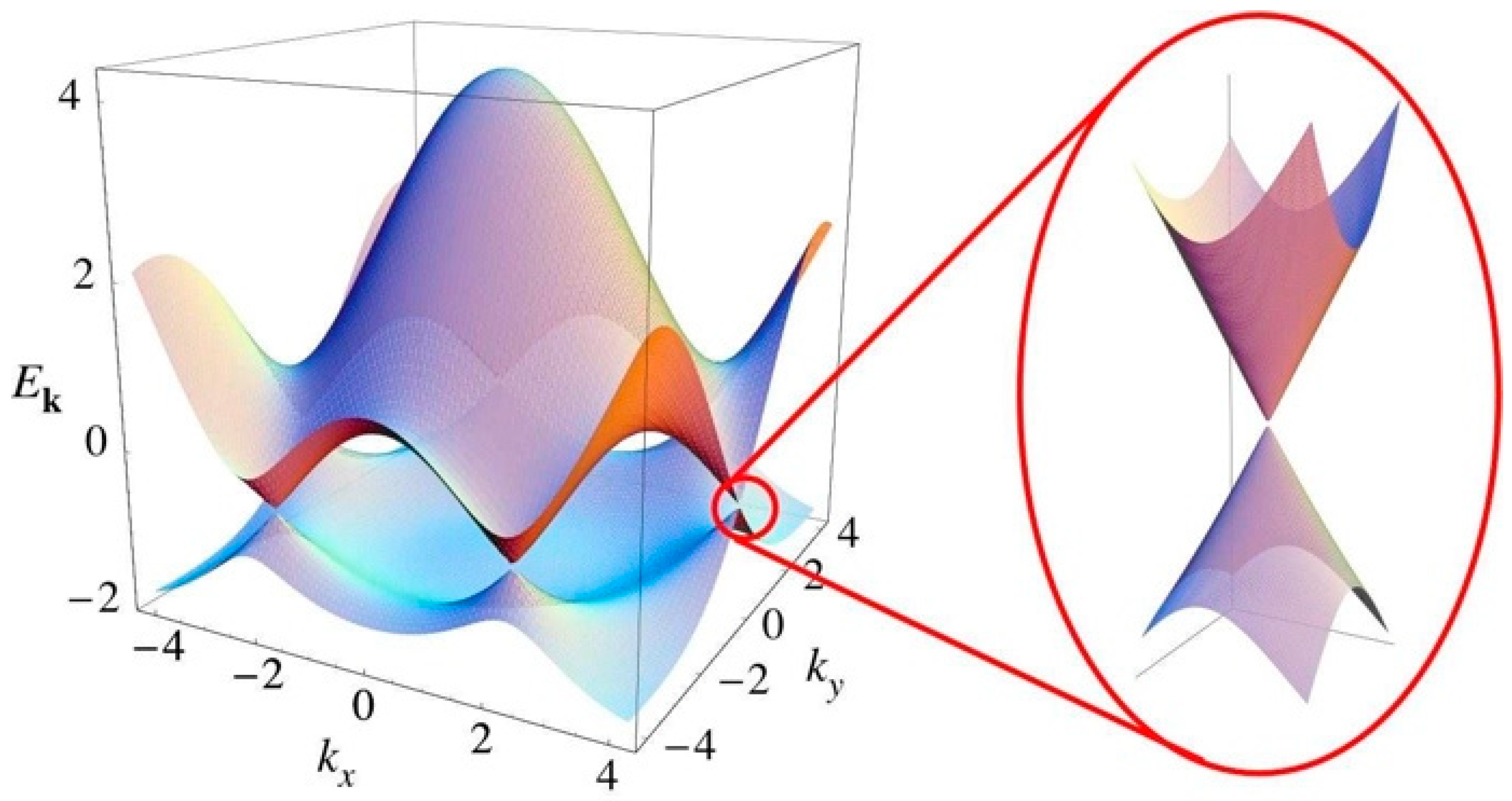
:1. Introduction
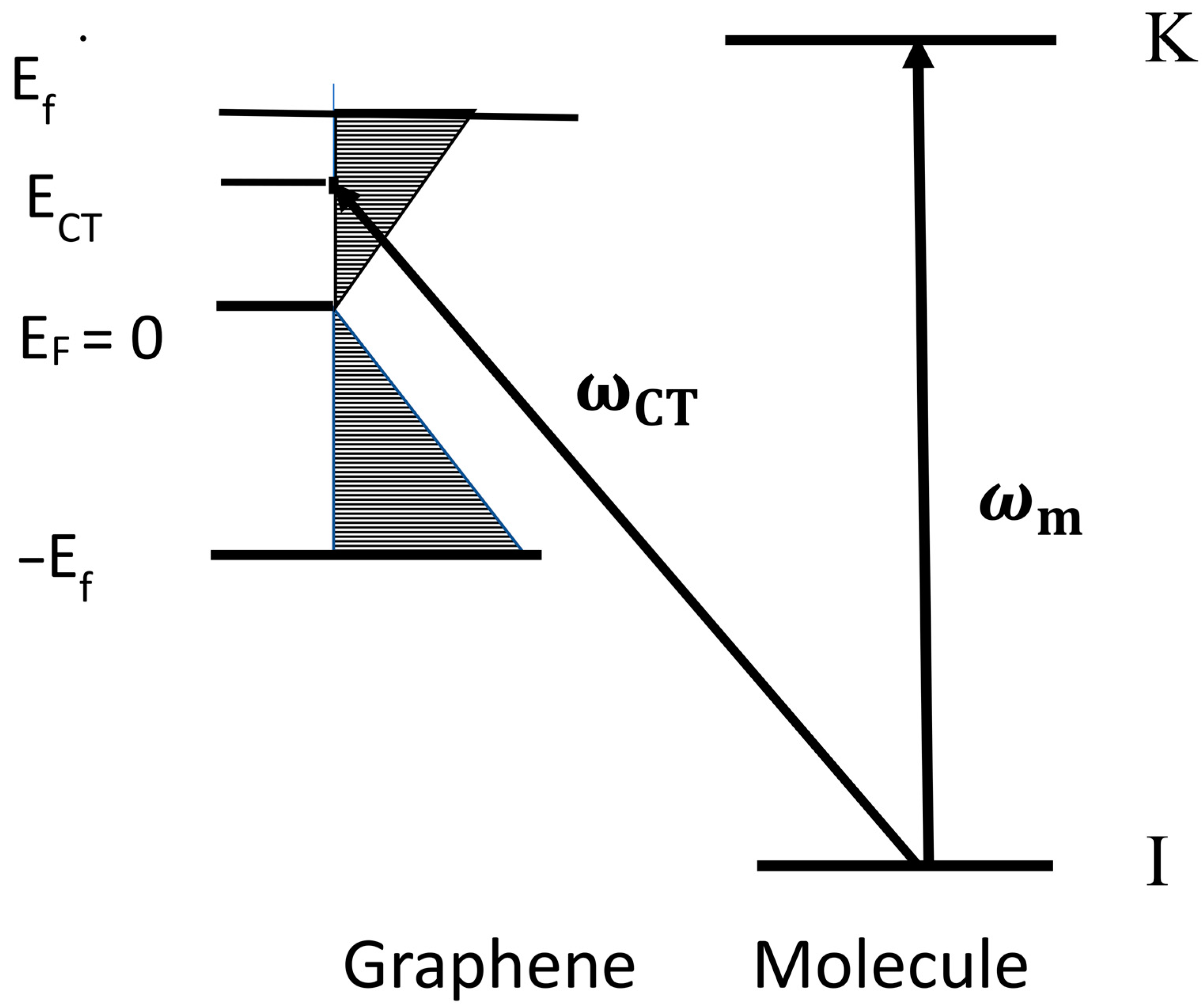
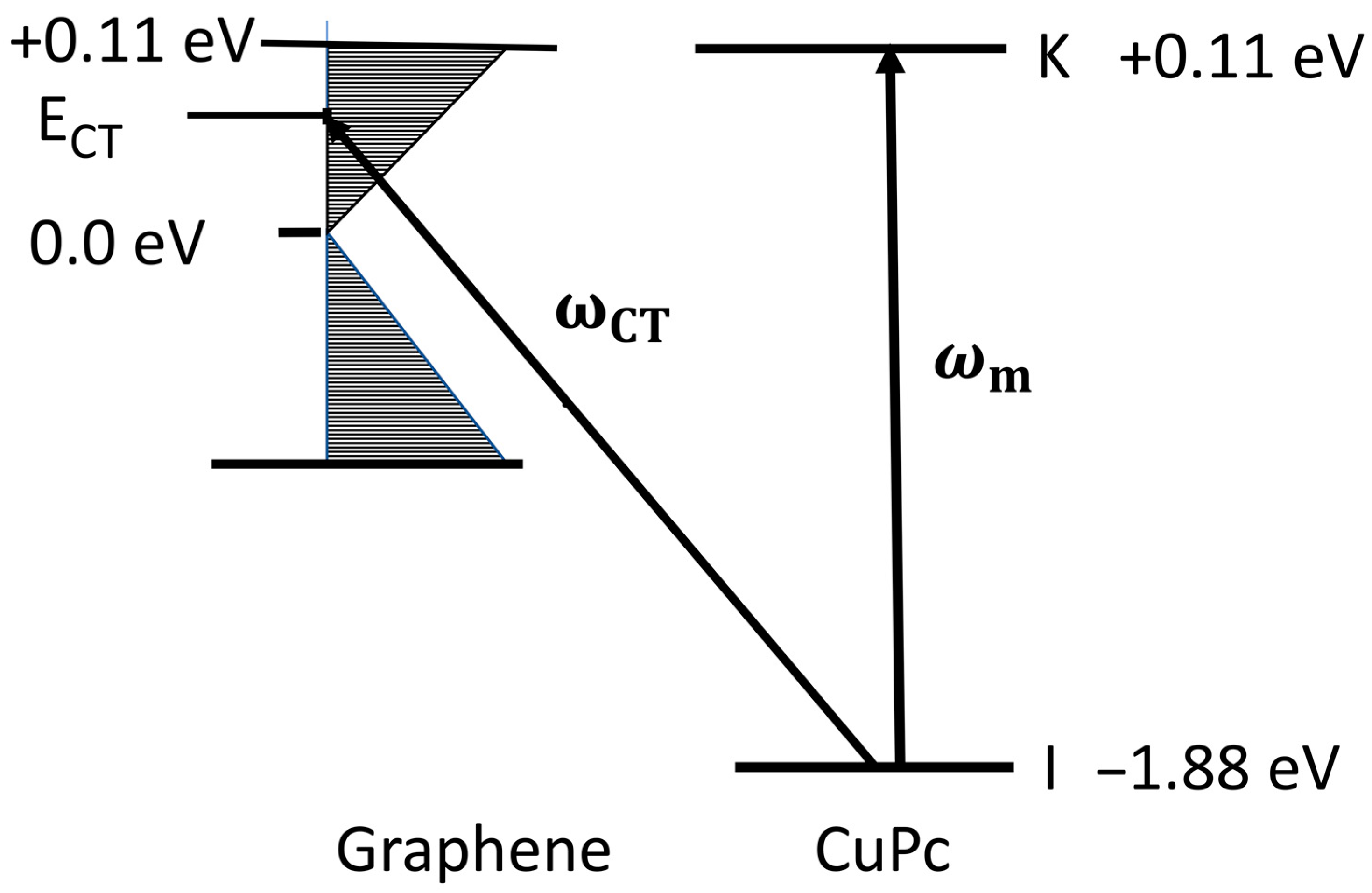
2. Optimum SERS Intensities from a Molecule Adsorbed on Mono-Layer Graphene
3. Discussion
Funding
Data Availability Statement
Conflicts of Interest
References and Note
- Van Duyne, R.P. Surface Enhanced Raman Scattering. In Chemical and Biochemical Applications of Lasers; Moore, C.B., Ed.; Academic Press: New York, NY, USA, 1979; Volume 4, p. 101. [Google Scholar]
- Kneipp, K.; Wang, Y.; Kneipp, H.; Perelman, L.T.; Itzkan, I.; Dasari, R.R.; Feld, M.S. Single Molecule Detection Using Surface-Enhanced Raman Scattering (SERS). Phys. Rev. Lett. 1997, 78, 1667–1670. [Google Scholar] [CrossRef] [Green Version]
- Lombardi, J.R.; Birke, R.L. A Unified Approach to Surface-Enhanced Raman Spectroscopy. J. Phys. Chem. C 2008, 112, 5605–5617. [Google Scholar] [CrossRef]
- Lombardi, J.R.; Birke, R.L.; Lu, T.; Xu, J. Charge-transfer theory of surface enhanced Raman spectroscopy: Herzberg–Teller contributions. J. Chem. Phys. 1986, 84, 4174–4180. [Google Scholar] [CrossRef]
- Quagliano, L.G. Observation of Molecules Adsorbed on III−V Semiconductor Quantum Dots by Surface Enhanced Raman Scattering. J. Am. Chem. Soc. 2004, 126, 7393–7398. [Google Scholar] [CrossRef]
- Lombardi, J.R.; Birke, R.L. Theory of Surface-Enhanced Raman Scattering in Semiconductors. J. Phys. Chem. C 2014, 118, 11120–11130. [Google Scholar] [CrossRef]
- Yilmaz, M.; Babur, E.; Ozdemir, M.; Gieseking, R.L.; Dede, Y.; Tamer, U.; Schatz, G.C.; Facchetti, A.; Usta, H.; Demirel, G. Nanostructured organic semiconductor films for molecular detection with surface-enhanced Raman spectroscopy. Nat. Mater. 2017, 16, 918–924. [Google Scholar] [CrossRef]
- Lombardi, J.R. Raman Spectroscopy Enhanced by Organic Semiconductors. Nat. Mater. 2017, 16, 878–880. [Google Scholar] [CrossRef]
- Cong, S.; Liu, X.; Jiang, Y.; Zhang, W.; Zhao, Z. Surface Enhanced Raman Scattering Revealed by Interfacial Charge-Transfer Transitions. Innov. Rev. 2020, 1, 100051. [Google Scholar] [CrossRef]
- Lombardi, J.R. The theory of surface-enhanced Raman scattering on semiconductor nanoparticles; toward the optimization of SERS sensors. Faraday Discuss. 2017, 205, 105–120. [Google Scholar] [CrossRef]
- Ling, X.; Fang, W.; Lee, Y.-H.; Araujo, P.T.; Zhang, X.; Rodriguez-Nieva, J.F.; Lin, Y.X.; Zhang, J.; Kong, J.; Dresselhaus, M.S. Raman Enhancement Effect on Two-Dimensional Layered Materials: Graphene, h-BN and MoS2. Nano Lett. 2014, 14, 3033–3040. [Google Scholar] [CrossRef]
- Ling, X.; Xie, L.; Fang, Y.; Xu, H.; Zhang, H.; Kong, J.; Dresselhaus, M.S.; Zhang, J.; Liu, Z. Can Graphene be used as a Substrate for Raman Enhancement? Nano Lett. 2010, 10, 553–561. [Google Scholar] [CrossRef] [PubMed]
- Liu, M.; Chen, W. Graphene nanosheets-supported Ag nanoparticles for ultrasensitive detection of TNT by surface-enhanced Raman spectroscopy. Biosens. Bioelectron. 2013, 46, 68–73. [Google Scholar] [CrossRef] [PubMed]
- Xu, W.; Ling, X.; Xiao, J.; Dresselhaus, M.S.; Kong, J.; Xu, H.; Liu, Z.; Zhang, J. Surface enhanced Raman spectroscopy on a flat graphene surface. Proc. Natl. Acad. Sci. USA 2012, 109, 9281–9286. [Google Scholar] [CrossRef] [Green Version]
- Xu, W.; Mao, N.; Zhang, J. Graphene: A Platform for Surface-Enhanced Raman Spectroscopy. Small 2013, 9, 1206–1224. [Google Scholar] [CrossRef] [PubMed]
- Albrecht, A.C. On the Theory of Raman Intensities. J. Chem. Phys. 1961, 34, 1476. [Google Scholar] [CrossRef]
- Lombardi, J.R. The theory of surface-enhanced Raman spectroscopy on organic semiconductors: J-aggregates. Chem. Phys. Lett. 2020, 751, 137553. [Google Scholar] [CrossRef]
- Neto, A.C.; Guinea, F.; Peres, N.M.; Novoselov, K.S.; Geim, A.K. The Electronic Properties of Graphene. arXiv 2008, arXiv:0709.1163v2. [Google Scholar]
- Hou, X.; Tang, X.; Wei, Y.; Wang, S.; Hao, Q.; Hou, J.-M.; Qiu, T. Role of dispersion relation effect in topological surface-enhanced Raman scattering. Cell Rep. Phys. Sci. 2021, 2, 100488. [Google Scholar] [CrossRef]
- Note, in most SERS studies it is common to take the origin of the energy to be the vacuum level. Thus, the ionization potential of the molecule is the energy of the HOMO. We nevertheless follow here the most common scaling of Graphene studies such that the Dirac point is chosen as the energy origin.
- Fu, X.; Bei, F.; Wang, X.; O’Brien, S.; Lombardi, J.R. Excitation profile of surface-enhanced Raman scattering in graphene–metal nanoparticle-based derivatives. Nanoscale 2010, 2, 1461–1466. [Google Scholar] [CrossRef]
- Londero, P.S.; Leona, M.; Lombardi, J.R. Definitive evidence for linked resonances in surface-enhanced Raman scattering: Excitation profile of Cu phthalocyanine. Appl. Phys. Lett. 2013, 102, 111101. [Google Scholar] [CrossRef]
- Ling, X.; Moura, L.G.; Pimenta, M.A.; Zhang, J. Charge-Transfer Mechanism in Graphene-Enhanced Raman Scattering. J. Phys. Chem. C 2012, 116, 25112–25118. [Google Scholar] [CrossRef]
- Ling, X.; Huang, S.; Deng, S.; Mao, N.; Kong, J.; Dresselhaus, M.S.; Zhang, J. Lighting Up the Raman Signal of Molecules in the Vicinity of Graphene Related Materials. Accounts Chem. Res. 2015, 48, 1862–1870. [Google Scholar] [CrossRef] [PubMed]
- Xiong, Z.; Meng, S.; Ma, X.; Gao, B.; Zhao, H. Dramatic n-Type Doping of Monolayer Graphene with Ferroelectric LiNbO3 Crystals and Bilayer Two-Dimensional Electron Gases. J. Phys. Chem. C 2022, 126, 4534–4541. [Google Scholar] [CrossRef]
Publisher’s Note: MDPI stays neutral with regard to jurisdictional claims in published maps and institutional affiliations. |
© 2022 by the author. Licensee MDPI, Basel, Switzerland. This article is an open access article distributed under the terms and conditions of the Creative Commons Attribution (CC BY) license (https://creativecommons.org/licenses/by/4.0/).
Share and Cite
Lombardi, J.R. The Theory of Surface-Enhanced Raman Spectroscopy on Organic Semiconductors: Graphene. Nanomaterials 2022, 12, 2737. https://doi.org/10.3390/nano12162737
Lombardi JR. The Theory of Surface-Enhanced Raman Spectroscopy on Organic Semiconductors: Graphene. Nanomaterials. 2022; 12(16):2737. https://doi.org/10.3390/nano12162737
Chicago/Turabian StyleLombardi, John R. 2022. "The Theory of Surface-Enhanced Raman Spectroscopy on Organic Semiconductors: Graphene" Nanomaterials 12, no. 16: 2737. https://doi.org/10.3390/nano12162737
APA StyleLombardi, J. R. (2022). The Theory of Surface-Enhanced Raman Spectroscopy on Organic Semiconductors: Graphene. Nanomaterials, 12(16), 2737. https://doi.org/10.3390/nano12162737