
Tunable Spin and Orbital Edelstein Effect at (111) LaAlO3/SrTiO3 Interface

 , and
, and 
Abstract
:1. Introduction
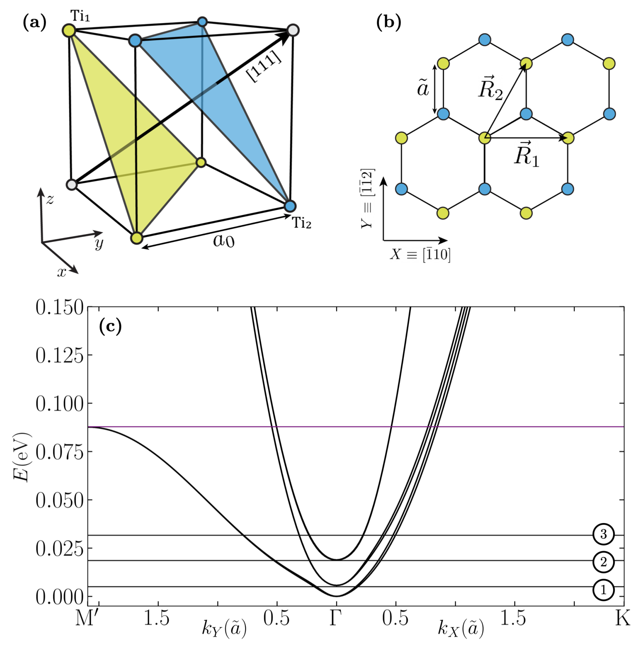
2. Methods
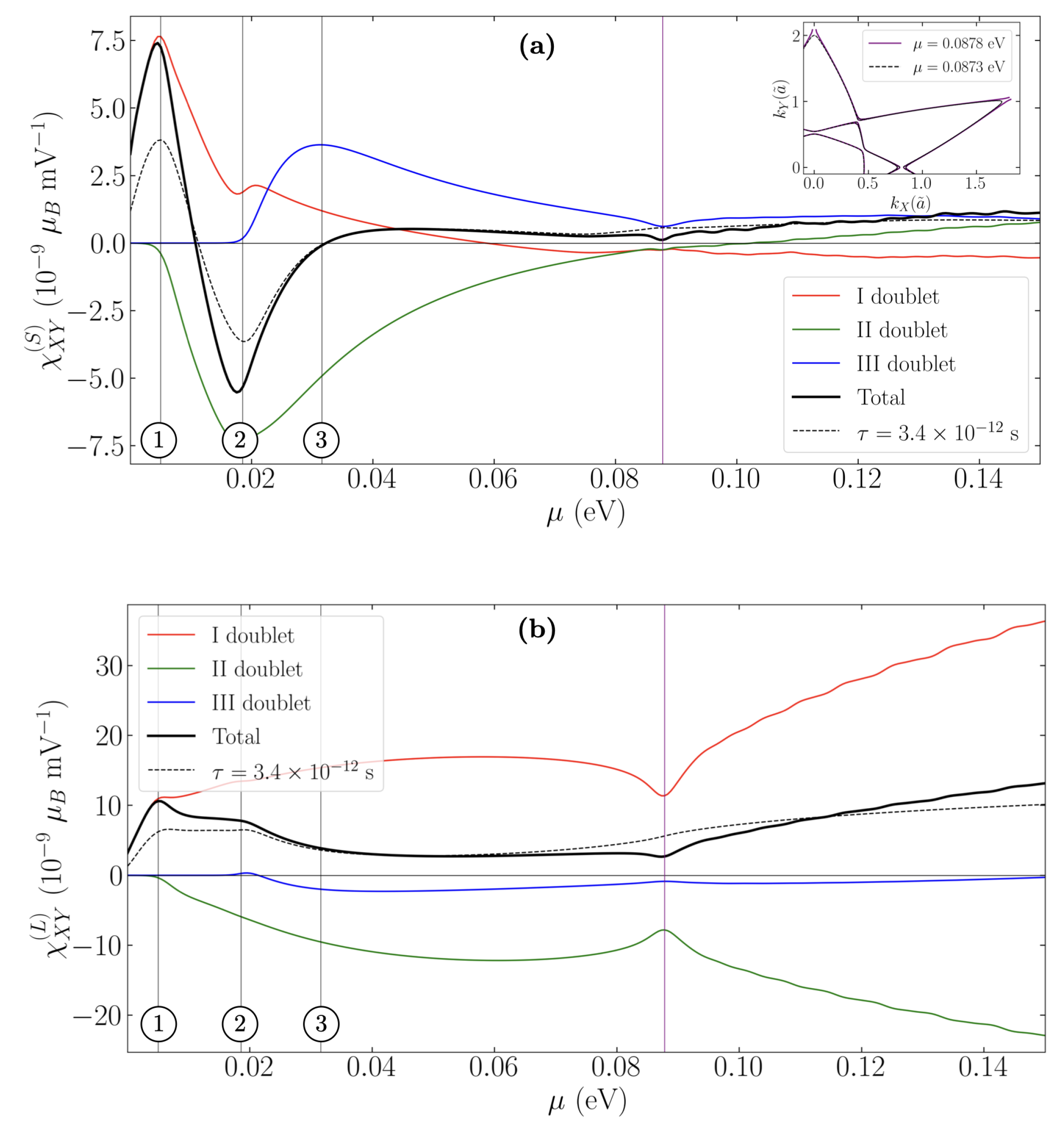
3. Discussion
Author Contributions
Funding
Acknowledgments
Conflicts of Interest
Abbreviations
| EE | Edelstein effect |
| SOC | spin–orbit coupling |
| 2DEG | two-dimensional electronic gas |
| STO | SrTiO |
| LAO | LaAlO |
| OEE | orbital Edelstein effect |
| TB | tight binding |
Appendix A. Details of the Model
Appendix A.1. Expansion at Low Fillings
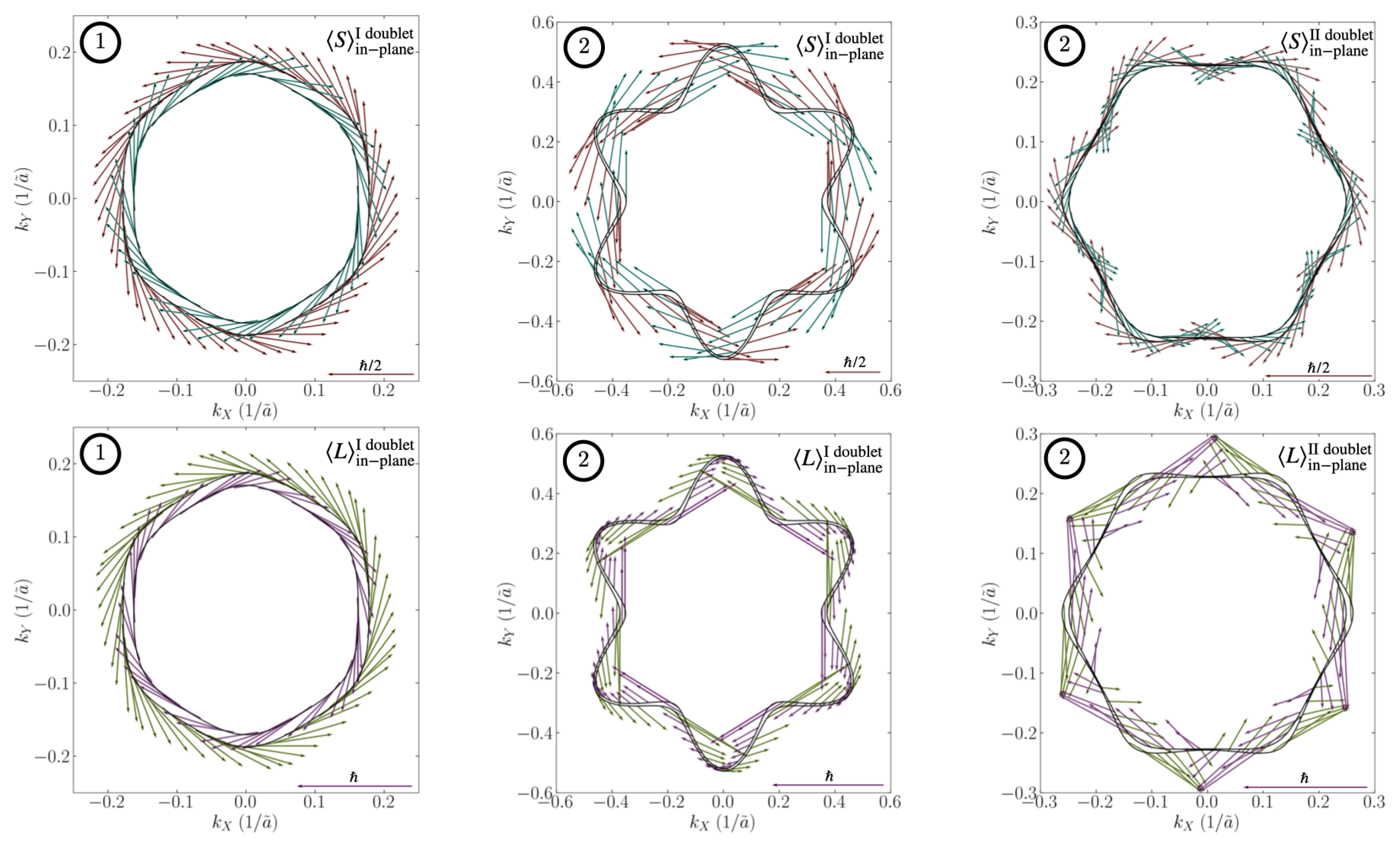
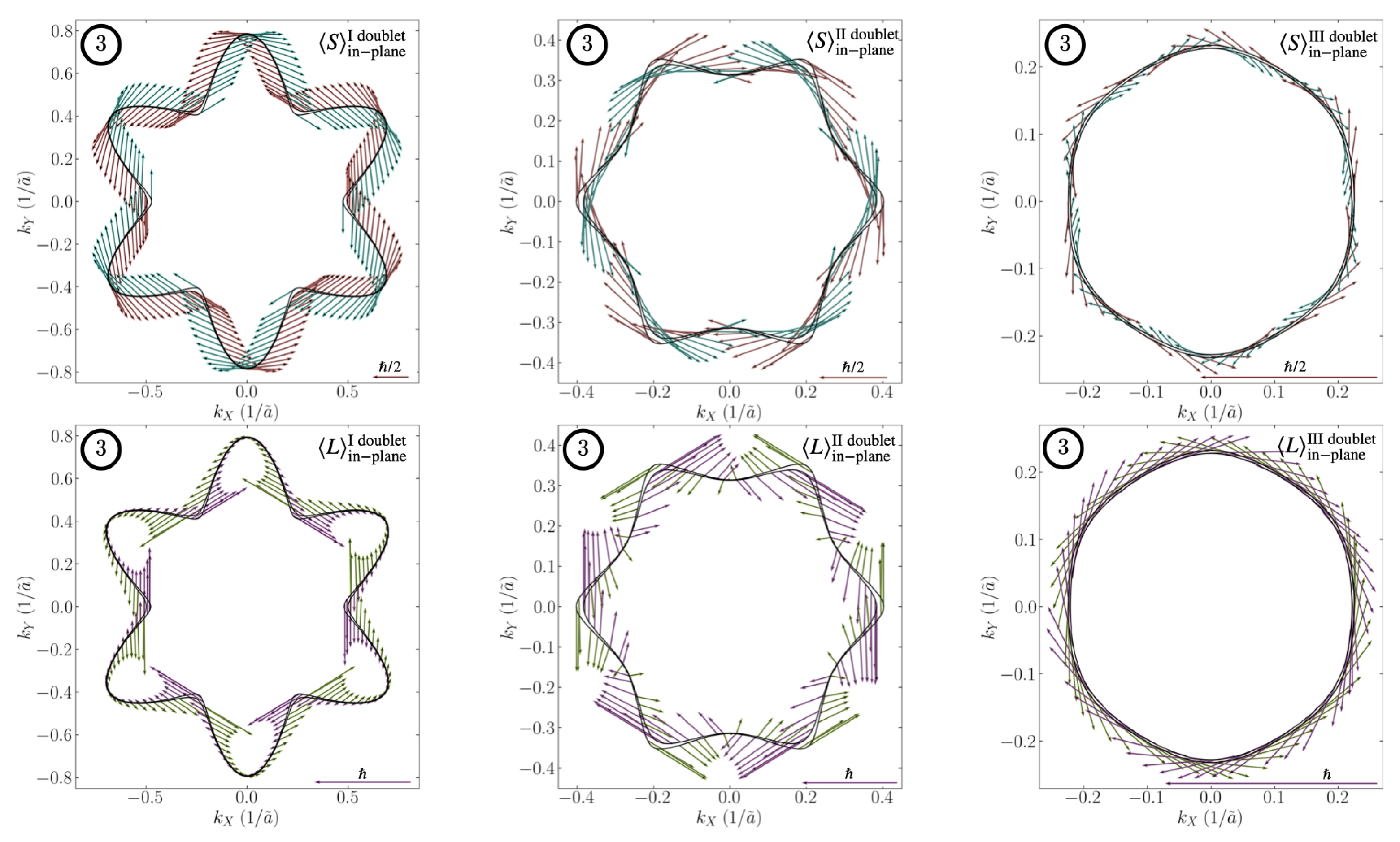
Appendix B. Spin and Orbital Textures
Appendix C. Role of Impurities Scattering on the Edelstein Effect

References
- Dieny, B.; Prejbeanu, I.L.; Garello, K.; Gambardella, P.; Freitas, P.; Lehndorff, R.; Raberg, W.; Ebels, U.; Demokritov, S.O.; Akerman, J.; et al. Opportunities and challenges for spintronics in the microelectronics industry. Nat. Electron. 2020, 3, 446–459. [Google Scholar] [CrossRef]
- Wolf, S.A.; Awschalom, D.D.; Buhrman, R.A.; Daughton, J.M.; Molnár, V.V.; Roukes, M.L.; Chtchelkanova, A.Y.; Treger, D.M. Spintronics: A spin-based electronics vision for the future. Science 2001, 294, 1488–1495. [Google Scholar] [CrossRef] [PubMed] [Green Version]
- Dyakonov, M.I.; Perel, V.I. Current-induced spin orientation of electrons in semiconductors. Phys. Lett. A 1971, 35, 459–460. [Google Scholar] [CrossRef]
- Edelstein, V.M. Spin polarization of conduction electrons induced by electric current in two-dimensional asymmetric electron systems. Solid State Commun. 1990, 73, 233–235. [Google Scholar] [CrossRef]
- Aronov, A.G.; Lyanda-Geller, Y.B. Nuclear electric resonance and orientation of carrier spins by an electric field. Sov. Phys. JETP 1989, 50, 431. [Google Scholar]
- Lin, W.; Li, L.; Doğan, F.; Li, C.; Rotella, H.; Yu, X.; Zhang, B.; Li, Y.; Lew, W.S.; Wang, S.; et al. Interface-based tuning of rashba spin-orbit interaction in asymmetric oxide heterostructures with 3d electrons. Nat. Commun. 2019, 10, 3052. [Google Scholar] [CrossRef] [PubMed]
- Hwang, H.Y.; Iwasa, Y.; Kawasaki, M.; Keimer, B.; Nagaosa, N.; Tokura, Y. Emergent phenomena at oxide interfaces. Nat. Mater. 2012, 11, 103–113. [Google Scholar] [CrossRef] [Green Version]
- Caviglia, A.D.; Gabay, M.; Gariglio, S.; Reyren, N.; Cancellieri, C.; Triscone, J.-M. Tunable rashba spin-orbit interaction at oxide interfaces. Phys. Rev. Lett. 2010, 104, 126803. [Google Scholar] [CrossRef] [Green Version]
- Gariglio, S.; Caviglia, A.D.; Triscone, J.; Gabay, M. A spin–orbit playground: Surfaces and interfaces of transition metal oxides. Rep. Prog. Phys. 2018, 82, 012501. [Google Scholar] [CrossRef] [Green Version]
- Pai, Y.; Tylan-Tyler, A.; Irvin, P.; Levy, J. Physics of SrTiO3-based heterostructures and nanostructures: A review. Rep. Prog. Phys. 2018, 81, 036503. [Google Scholar] [CrossRef] [Green Version]
- Vivek, M.O.G.M.; Gabay, M. Topological states at the (001) surface of SrTiO3. Phys. Rev. B 2017, 95, 165117. [Google Scholar] [CrossRef] [Green Version]
- Scheurer, M.S.; Schmalian, J. Topological superconductivity and unconventional pairing in oxide interfaces. Nat. Commun. 2015, 6, 6005. [Google Scholar] [CrossRef] [PubMed] [Green Version]
- Mohanta, N.; Taraphder, A. Topological superconductivity and Majorana bound states at the LaAlO3/SrTiO3 interface. EPL 2014, 108, 60001. [Google Scholar] [CrossRef] [Green Version]
- Loder, F.; Kampf, A.P.; Kopp, T. Route to topological superconductivity via magnetic field rotation. Sci. Rep. 2015, 5, 15302. [Google Scholar] [CrossRef] [PubMed] [Green Version]
- Fukaya, Y.; Tamura, S.; Yada, K.; Tanaka, Y.; Gentile, P.; Cuoco, M. Interorbital topological superconductivity in spin-orbit coupled superconductors with inversion symmetry breaking. Phys. Rev. B 2018, 97, 174522. [Google Scholar] [CrossRef] [Green Version]
- Fidkowski, L.; Lutchyn, R.M.; Nayak, C.; Fisher, M.P.A. Majorana zero modes in one-dimensional quantum wires without long-ranged superconducting order. Phys. Rev. B 2011, 84, 195436. [Google Scholar] [CrossRef] [Green Version]
- Fidkowski, L.; Jiang, H.; Lutchyn, R.M.; Nayak, C. Magnetic and superconducting ordering in one-dimensional nanostructures at the LaAlO3/SrTiO3 interface. Phys. Rev. B 2013, 87, 014436. [Google Scholar] [CrossRef] [Green Version]
- Mazziotti, M.V.; Scopigno, N.; Grilli, M.; Caprara, S. Majorana Fermions in One-Dimensional Structures at LaAlO3/SrTiO3 Oxide Interfaces. Condens. Matter 2018, 3, 37. [Google Scholar] [CrossRef] [Green Version]
- Perroni, C.A.; Cataudella, V.; Salluzzo, M.; Cuoco, M.; Citro, R. Evolution of topological superconductivity by orbital-selective confinement in oxide nanowires. Phys. Rev. B 2019, 100, 094526. [Google Scholar] [CrossRef] [Green Version]
- Settino, J.; Forte, F.; Perroni, C.A.; Cataudella, V.; Cuoco, M.; Citro, R. Spin-orbital polarization of majorana edge states in oxide nanowires. Phys. Rev. B 2020, 102, 224508. [Google Scholar] [CrossRef]
- Trier, F.; Vaz, D.C.; Bruneel, P.; Noël, P.; Fert, A.; Vila, L.; Attané, J.; Barthélémy, A.; Gabay, M.; Jaffrès, H.; et al. Electric-field control of spin current generation and detection in ferromagnet-free SrTiO3-based nanodevices. Nano Lett. 2019, 20, 395–401. [Google Scholar] [CrossRef] [PubMed]
- Johansson, A.; Göbel, B.; Henk, J.; Bibes, M.; Mertig, I. Spin and orbital edelstein effects in a two-dimensional electron gas: Theory and application to SrTiO3 interfaces. Phys. Rev. Res. 2021, 3, 013275. [Google Scholar] [CrossRef]
- Chirolli, L.; Mercaldo, M.T.; Guarcello, C.; Giazotto, F.; Cuoco, M. Colossal orbital edelstein effect in noncentrosymmetric superconductors. Phys. Rev. Lett. 2022, 128, 217703. [Google Scholar] [CrossRef] [PubMed]
- Levitov, L.S.; Nazarov, Y.V.; Eliashberg, G.M. Magnetoelectric effects in conductors with mirror isomer symmetry. Sov. Phys. JETP 1985, 61, 133. [Google Scholar]
- Go, D.; Jo, D.; Lee, H.; Kläui, M.; Mokrousov, Y. Orbitronics: Orbital currents in solids. EPL 2021, 135, 37001. [Google Scholar] [CrossRef]
- Chakhalian, J.; Liu, X.; Fiete, G.A. Strongly correlated and topological states in [111] grown transition metal oxide thin films and heterostructures. APL Mater. 2020, 8, 050904. [Google Scholar] [CrossRef]
- Xiao, D.; Zhu, W.; Ran, Y.; Nagaosa, N.; Okamoto, S. Interface engineering of quantum hall effects in digital transition metal oxide heterostructures. Nat. Commun. 2011, 2, 596. [Google Scholar] [CrossRef]
- Bruno, F.Y.; Walker, S.M.; Riccò, S.; Torre, A.D.L.; Wang, Z.; Tamai, A.; Kim, T.K.; Hoesch, M.; Bahramy, M.S.; Baumberger, F. Band structure and spin–orbital texture of the (111)-ktao3 2d electron gas. Adv. Electron. Mater. 2019, 5, 1800860. [Google Scholar] [CrossRef] [Green Version]
- Boudjada, N.; Wachtel, G.; Paramekanti, A. Magnetic and nematic orders of the two-dimensional electron gas at oxide (111) surfaces and interfaces. Phys. Rev. Lett. 2018, 120, 086802. [Google Scholar] [CrossRef] [Green Version]
- Rout, P.K.; Agireen, I.; Maniv, E.; Goldstein, M.; Dagan, Y. Six-fold crystalline anisotropic magnetoresistance in the (111) LaAlO3/SrTiO3 oxide interface. Phys. Rev. B 2017, 95, 241107. [Google Scholar] [CrossRef] [Green Version]
- Monteiro, A.M.R.V.L.; Groenendijk, D.J.; Groen, I.; de Bruijckere, J.; Gaudenzi, R.; Zant, H.S.J.V.D.; Caviglia, A.D. Two-dimensional superconductivity at the (111) LaAlO3/SrTiO3 interface. Phys. Rev. B 2017, 96, 020504. [Google Scholar] [CrossRef] [Green Version]
- Davis, S.; Huang, Z.; Han, K.; Venkatesan, T.; Chandrasekhar, V. Magnetoresistance in the superconducting state at the (111) LaAlO3/SrTiO3 interface. Phys. Rev. B 2017, 96, 134502. [Google Scholar] [CrossRef] [Green Version]
- Doennig, D.; Pickett, W.E.; Pentcheva, R. Massive Symmetry Breaking in LaAlO3/SrTiO3 (111) Quantum Wells: A Three-Orbital Strongly Correlated Generalization of Graphene. Phys. Rev. Lett. 2013, 111, 126804. [Google Scholar] [CrossRef] [PubMed] [Green Version]
- Khanna, U.; Rout, P.K.; Mograbi, M.; Tuvia, G.; Leermakers, I.; Zeitler, U.; Dagan, Y.; Goldstein, M. Symmetry and Correlation Effects on Band Structure Explain the Anomalous Transport Properties of (111) LaAlO3/SrTiO3. Phys. Rev. Lett. 2019, 123, 036805. [Google Scholar] [CrossRef] [PubMed] [Green Version]
- He, P.; Walker, S.M.; Zhang, S.S.; Bruno, F.Y.; Bahramy, M.S.; Lee, J.M.; Ramaswamy, R.; Cai, K.; Heinonen, O.; Vignale, G.; et al. Observation of out-of-plane spin texture in a SrTiO3 (111) two-dimensional electron gas. Phys. Rev. Lett. 2018, 120, 266802. [Google Scholar] [CrossRef] [Green Version]
- Trama, M.; Cataudella, V.; Perroni, C.A. Strain-induced topological phase transition at (111) SrTiO3-based heterostructures. Phys. Rev. Res. 2021, 3, 043038. [Google Scholar] [CrossRef]
- Trama, M.; Perroni, C.A.; Cataudella, V.; Romeo, F.; Citro, R. Gate tunable anomalous Hall effect at (111) LaAlO3/SrTiO3 interface. arXiv 2022, arXiv:2202.04664. [Google Scholar]
- Keppler, H. Crystal Field Theory; Springer: Dordrecht, The Netherlands, 1998; pp. 118–120. [Google Scholar]
- Monteiro, A.M.R.V.L.; Vivek, M.; Groenendijk, D.J.; Bruneel, P.; Leermakers, I.; Zeitler, U.; Gabay, M.; Caviglia, A.D. Band inversion driven by electronic correlations at the (111) LaAlO3/SrTiO3 interface. Phys. Rev. B 2019, 99, 201102. [Google Scholar] [CrossRef] [Green Version]
- Luca, G.M.D.; Capua, R.D.; Gennaro, E.D.; Sambri, A.; Granozio, F.M.; Ghiringhelli, G.; Betto, D.; Piamonteze, C.; Brookes, N.B.; Salluzzo, M. Symmetry breaking at the (111) interfaces of SrTiO3 hosting a two-dimensional electron system. Phys. Rev. B 2018, 98, 115143. [Google Scholar] [CrossRef] [Green Version]
- Shen, K.; Vignale, G.; Raimondi, R. Microscopic theory of the inverse edelstein effect. Phys. Rev. Lett. 2014, 112, 096601. [Google Scholar] [CrossRef] [Green Version]
- Khan, T.; Zhang, H.; Zhang, H.; Yan, X.; Hong, D.; Han, F.; Chen, Y.; Shen, B.; Sun, J. High mobility 2-dimensional electron gas at LaAlO3/SrTiO3 interface prepared by spin coating chemical methods. Nanotechnology 2017, 28, 435701. [Google Scholar] [CrossRef] [PubMed] [Green Version]
- Bhowal, S.; Vignale, G. Orbital hall effect as an alternative to valley hall effect in gapped graphene. Phys. Rev. B 2021, 103, 195309. [Google Scholar] [CrossRef]
- Bareille, C.; Fortuna, F.; Rödel, T.C.; Bertran, F.; Gabay, M.; Cubelos, O.H.; Taleb-Ibrahimi, A.; Fevre, P.L.; Bibes, M.; Barthélémy, A.; et al. Two-dimensional electron gas with six-fold symmetry at the (111) surface of KTaO3. Sci. Rep. 2014, 4, 3586. [Google Scholar] [CrossRef] [PubMed] [Green Version]
- Vicente-Arche, L.M.; Bréhin, J.; Varotto, S.; Cosset-Cheneau, M.; Mallik, S.; Salazar, R.; Noël, P.; Vaz, D.C.; Trier, F.; Bhattacharya, S.; et al. Spin–charge interconversion in KTaO3 2D electron gases. Adv. Mater. 2021, 33, 2102102. [Google Scholar] [CrossRef]
- Khomskii, D. Transition Metal Compounds; Cambridge University Press: Cambridge, UK, 2014. [Google Scholar]
- Kalabukhov, A.; Gunnarsson, R.; Börjesson, J.; Olsson, E.; Claeson, T.; Winkler, D. Effect of oxygen vacancies in the SrTiO3 substrate on the electrical properties of the LaAlO3/ SrTiO3 interface. Phys. Rev. B 2007, 75, 121404. [Google Scholar] [CrossRef] [Green Version]
- Li, Y.; Phattalung, S.N.; Limpijumnong, S.; Kim, J.; Yu, J. Formation of oxygen vacancies and charge carriers induced in the n-type interface of a LaAlO3 overlayer on SrTiO3 (001). Phys. Rev. B 2011, 84, 245307. [Google Scholar] [CrossRef]
- Walker, S.M.; Torre, A.D.L.; Bruno, F.Y.; Tamai, A.; Kim, T.K.; Hoesch, M.; Shi, M.; Bahramy, M.S.; King, P.D.C.; Baumberger, F. Control of a two-dimensional electron gas on SrTiO3 (111) by atomic oxygen. Phys. Rev. Lett. 2014, 113, 177601. [Google Scholar] [CrossRef] [Green Version]

Publisher’s Note: MDPI stays neutral with regard to jurisdictional claims in published maps and institutional affiliations. |
© 2022 by the authors. Licensee MDPI, Basel, Switzerland. This article is an open access article distributed under the terms and conditions of the Creative Commons Attribution (CC BY) license (https://creativecommons.org/licenses/by/4.0/).
Share and Cite
Trama, M.; Cataudella, V.; Perroni, C.A.; Romeo, F.; Citro, R. Tunable Spin and Orbital Edelstein Effect at (111) LaAlO3/SrTiO3 Interface. Nanomaterials 2022, 12, 2494. https://doi.org/10.3390/nano12142494
Trama M, Cataudella V, Perroni CA, Romeo F, Citro R. Tunable Spin and Orbital Edelstein Effect at (111) LaAlO3/SrTiO3 Interface. Nanomaterials. 2022; 12(14):2494. https://doi.org/10.3390/nano12142494
Chicago/Turabian StyleTrama, Mattia, Vittorio Cataudella, Carmine Antonio Perroni, Francesco Romeo, and Roberta Citro. 2022. "Tunable Spin and Orbital Edelstein Effect at (111) LaAlO3/SrTiO3 Interface" Nanomaterials 12, no. 14: 2494. https://doi.org/10.3390/nano12142494
APA StyleTrama, M., Cataudella, V., Perroni, C. A., Romeo, F., & Citro, R. (2022). Tunable Spin and Orbital Edelstein Effect at (111) LaAlO3/SrTiO3 Interface. Nanomaterials, 12(14), 2494. https://doi.org/10.3390/nano12142494