
Review on Perovskite Semiconductor Field–Effect Transistors and Their Applications

 ,
, 
Abstract
:1. Introduction
2. Fundamentals of Semiconducting Perovskite Semiconductor Materials
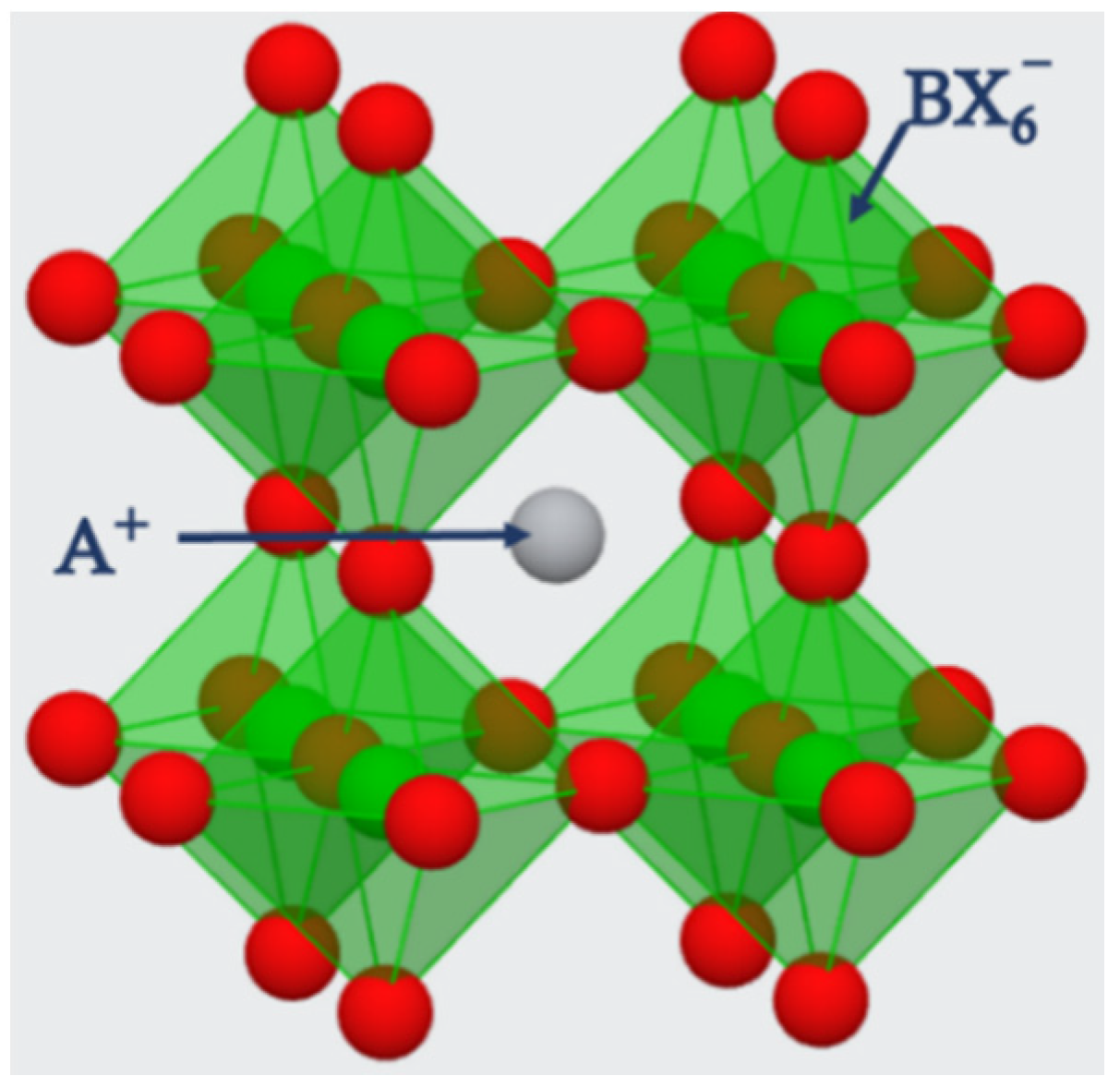
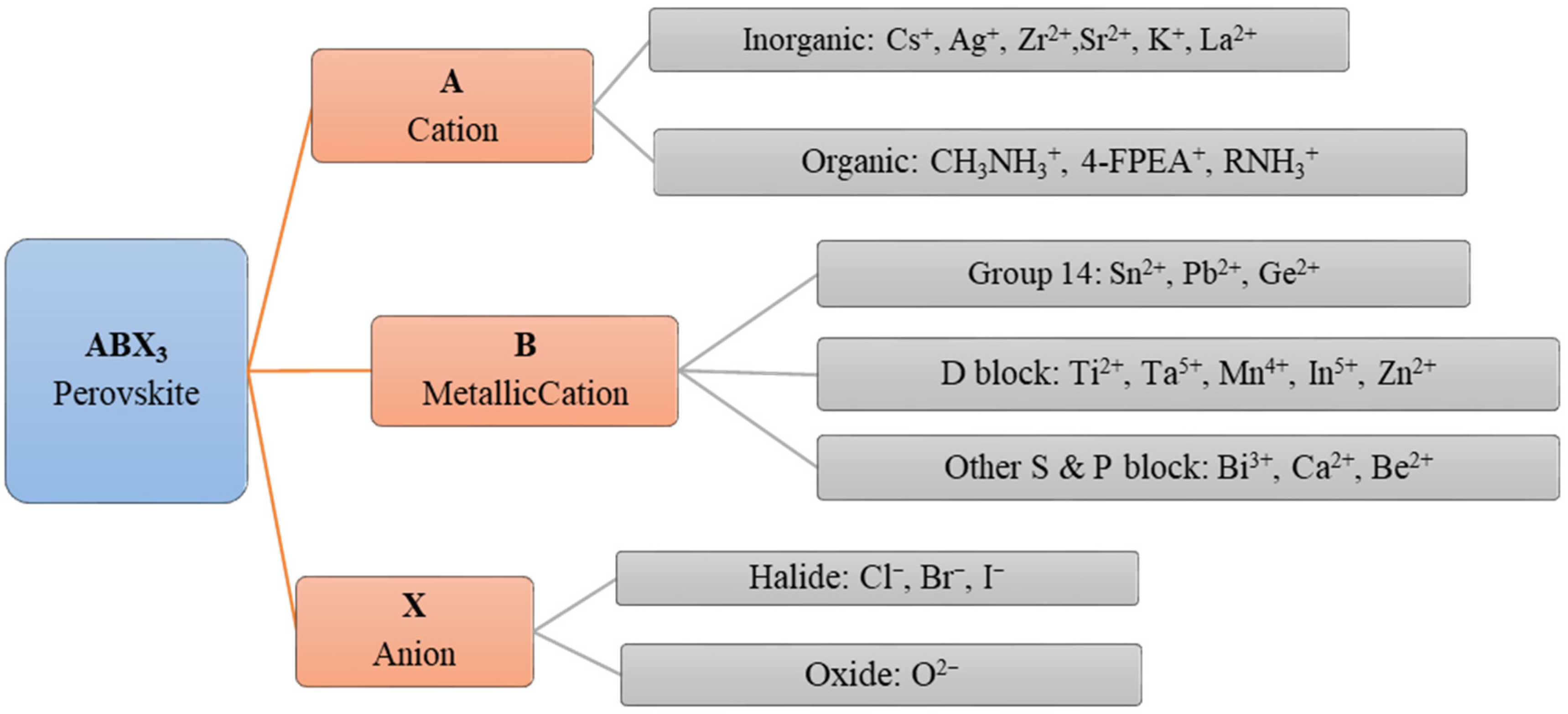
2.1. Hybrid Perovskites
2.2. All Inorganic Perovskites
2.3. Double and Triple Perovskites
3. Perovskite FETs
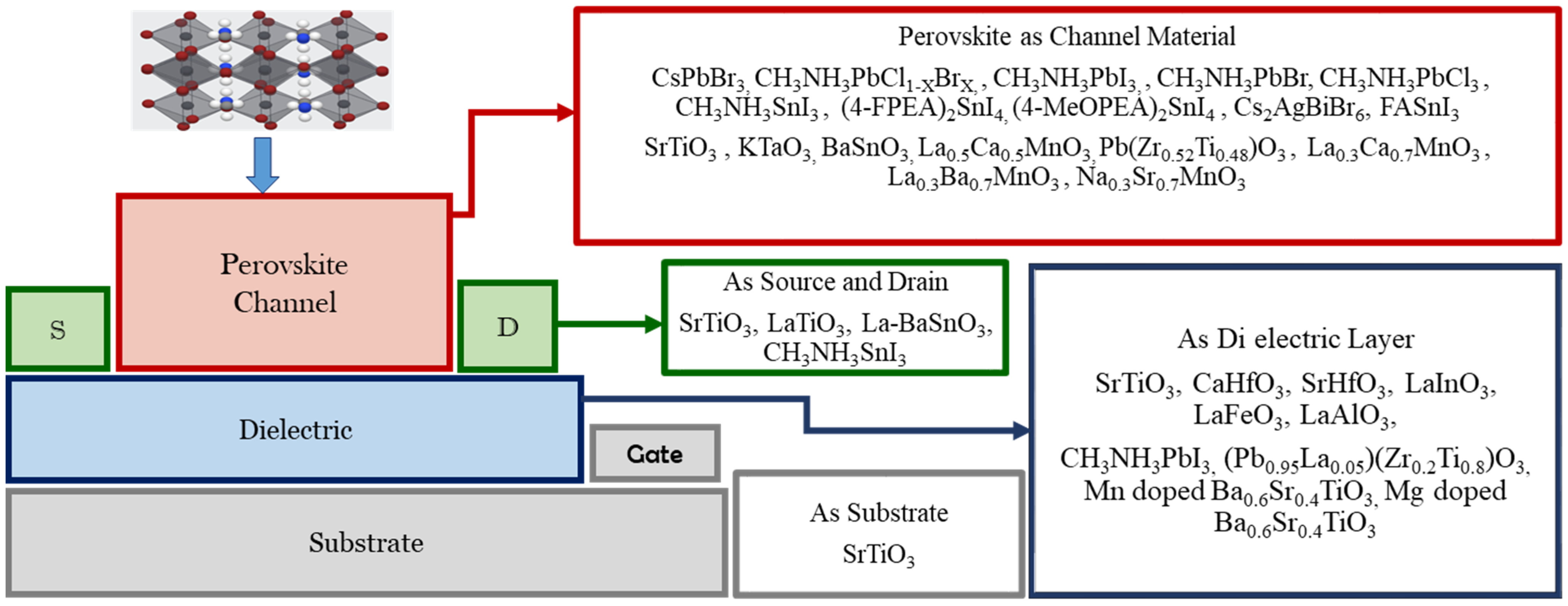
3.1. Perovskite Thin Film FET Device Structures
3.2. Electrical Properties of FETs
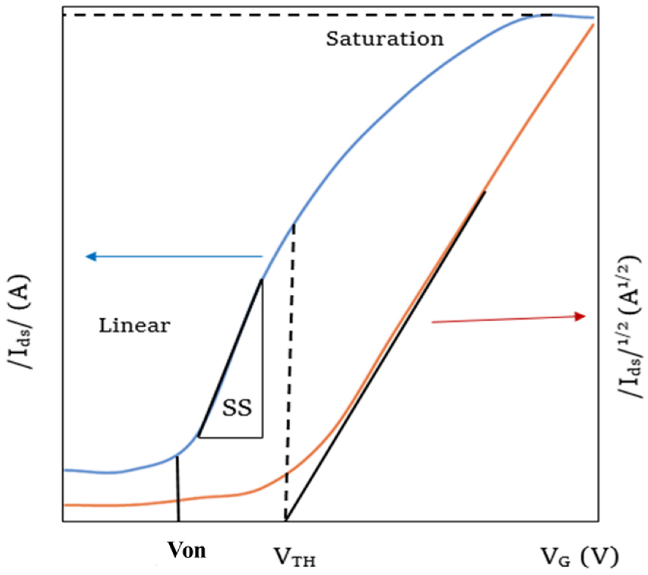
3.2.1. On-Off Ratio
3.2.2. Threshold Voltage
3.2.3. Mobility Calculations in FETs
3.3. Early Works (Before 2012) on Perovskite FETs
3.4. Recent Works (After 2012) on Perovskite FETs
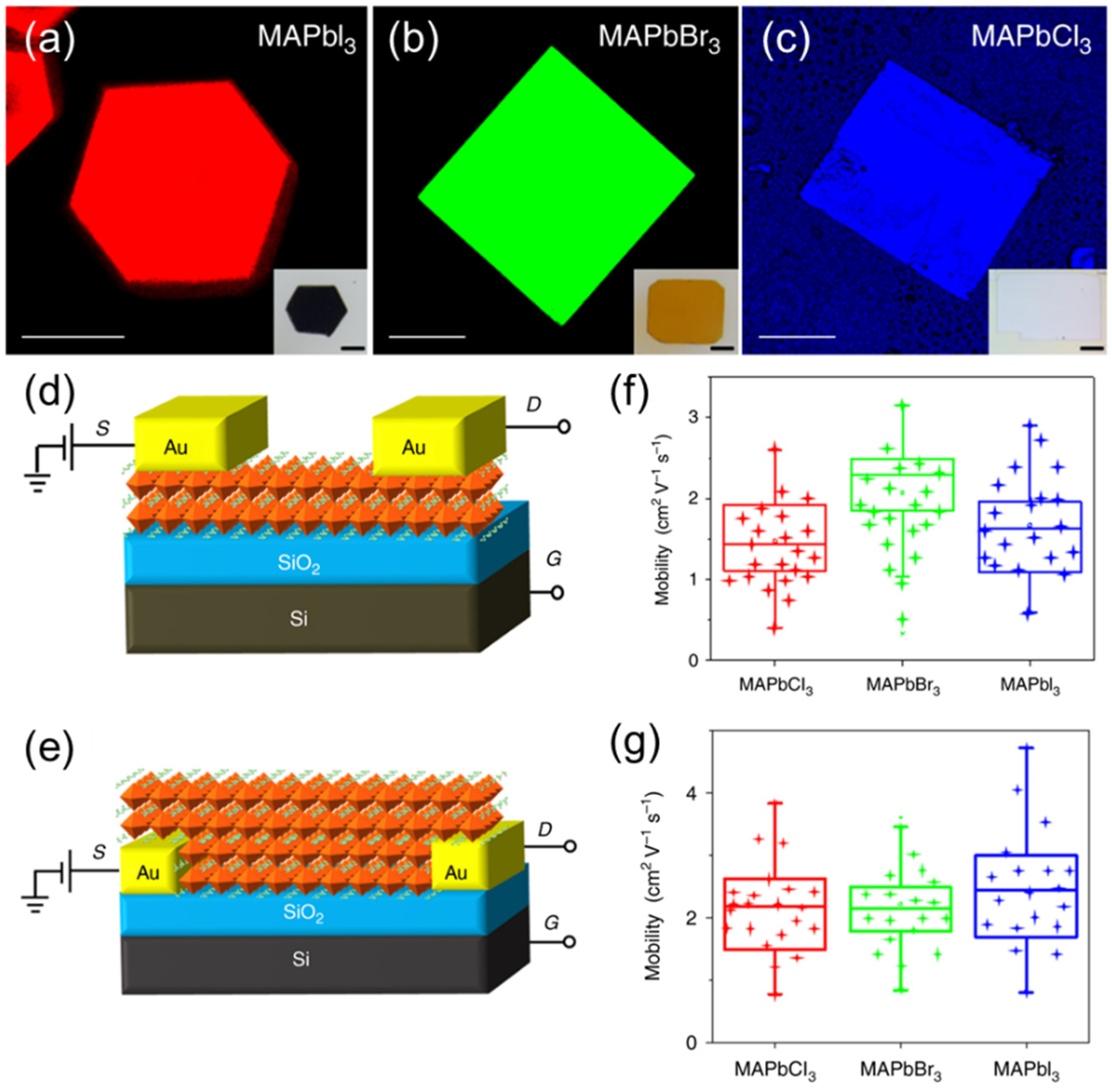
3.4.1. Hybrid (Organic Inorganic) Perovskite FETs
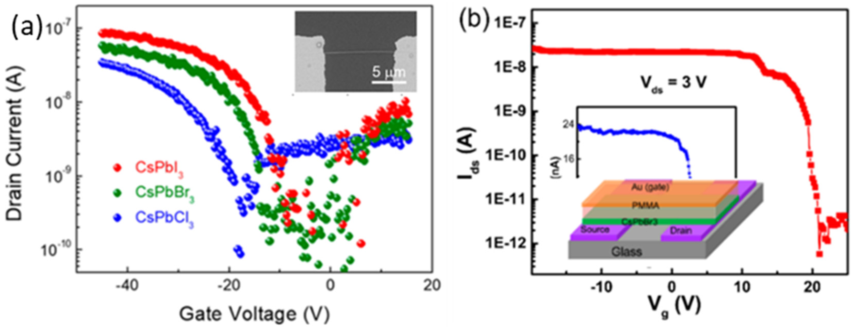
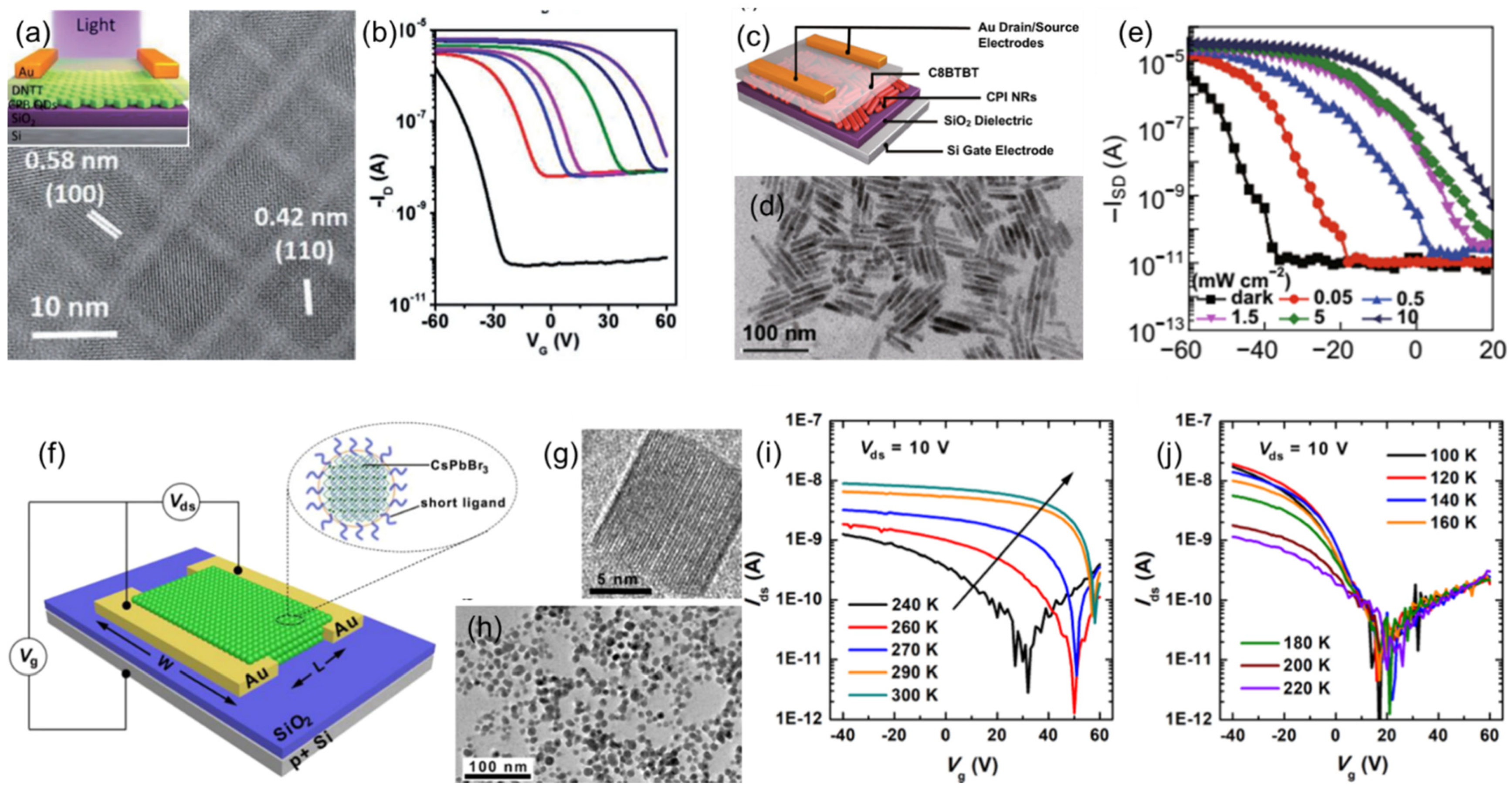
3.4.2. All-Inorganic Perovskite FETs
3.4.3. Double and Triple Perovskite FETs
3.5. Single Crystalline Perovskite FETs
3.6. Perovskite FETs with Nanostructured Channel
4. Applications of Perovskite FETs
4.1. FET Platforms as Tool for Evaluating the Carrier Mobility
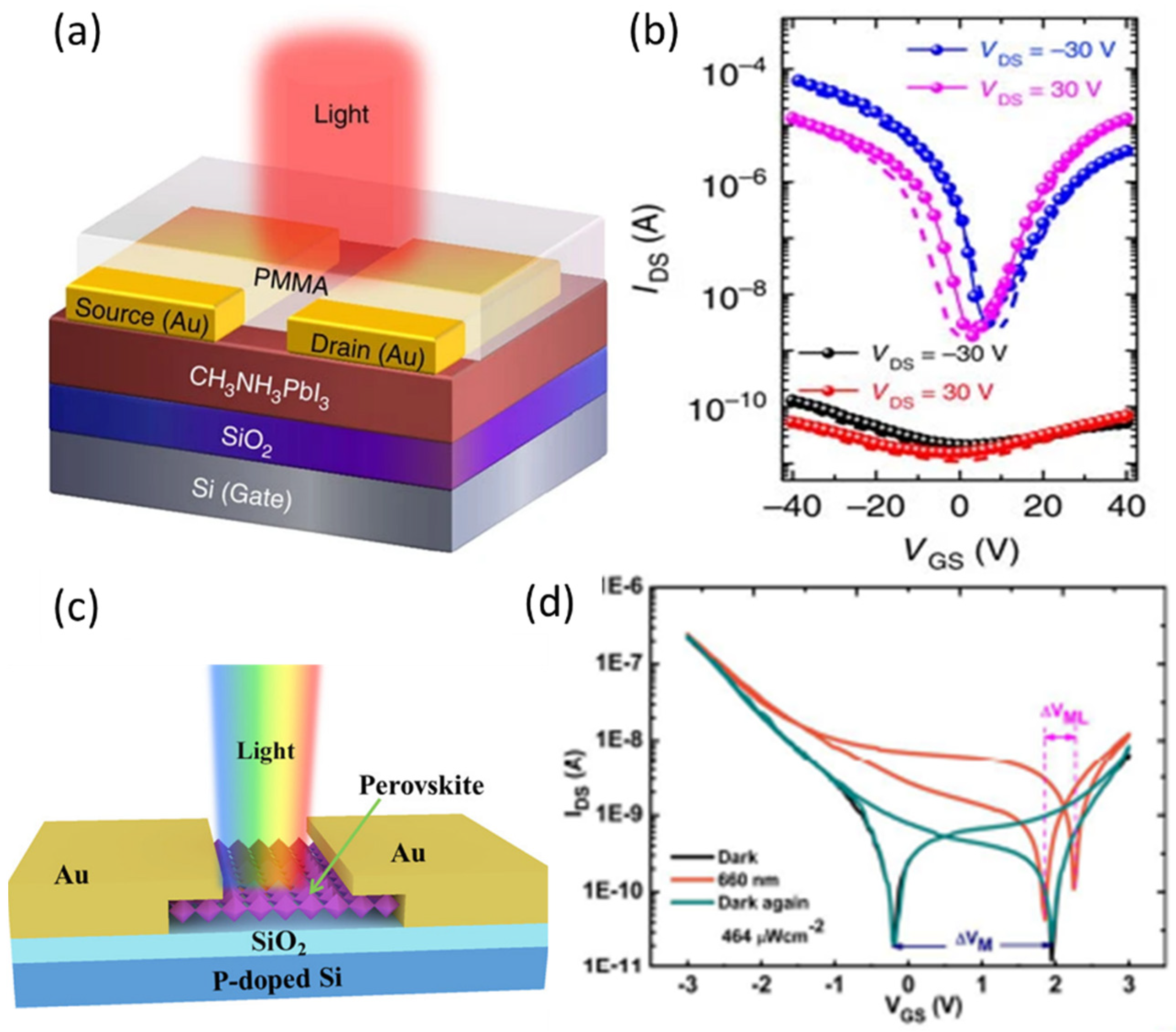
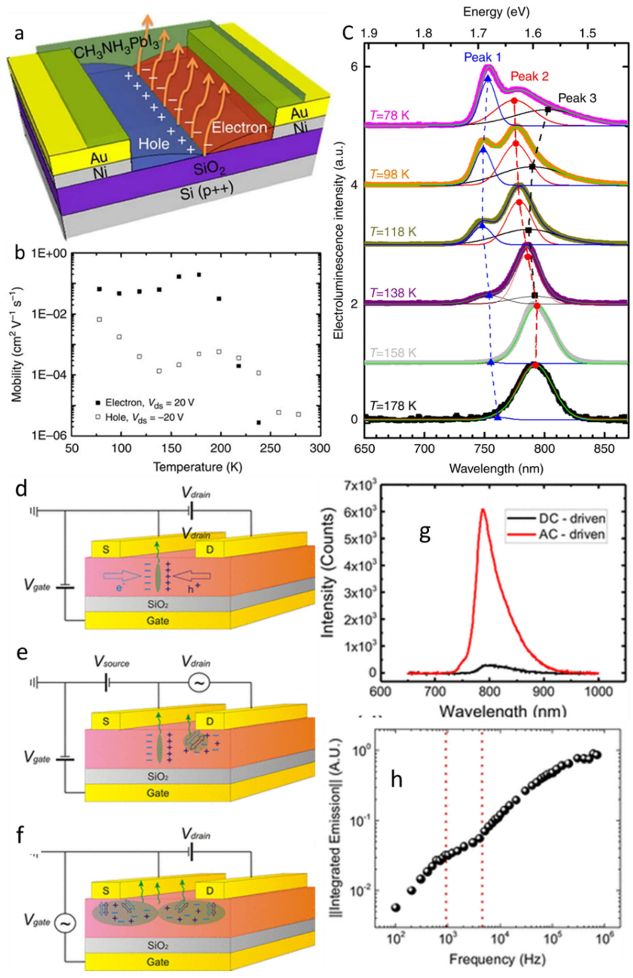
4.2. Photo FETs
4.3. Photo Detectors
4.4. LEFETS

| Perovskite | Hole Mobility (μ) cm2s−1V−1 | On/Off Ratio | Wavelength Peak nm | Ref |
|---|---|---|---|---|
| MAPbI3 | 0.072 at 78 K 0.00002 at 300 K | 106 | 800 | [20] |
| MAPbI3 | 0.025 at 78 K | 1000 | 783 | [102] |
| MAPbI3 | 0.025 at 78 K | 1000 | 783 | [187] |
| NFPI7 | 20 at 300 K | 106 | 800 | [188] |
| MAPbI3 Microplate | 4 at 77 K | 103 | 800 | [173] |
| CsPbBr3 NC/Poly fluorine | 3.3 at 250 K 5 at 100 K | 105 | 500 | [136] |
4.5. Ferroelectric RAM
5. Challenges
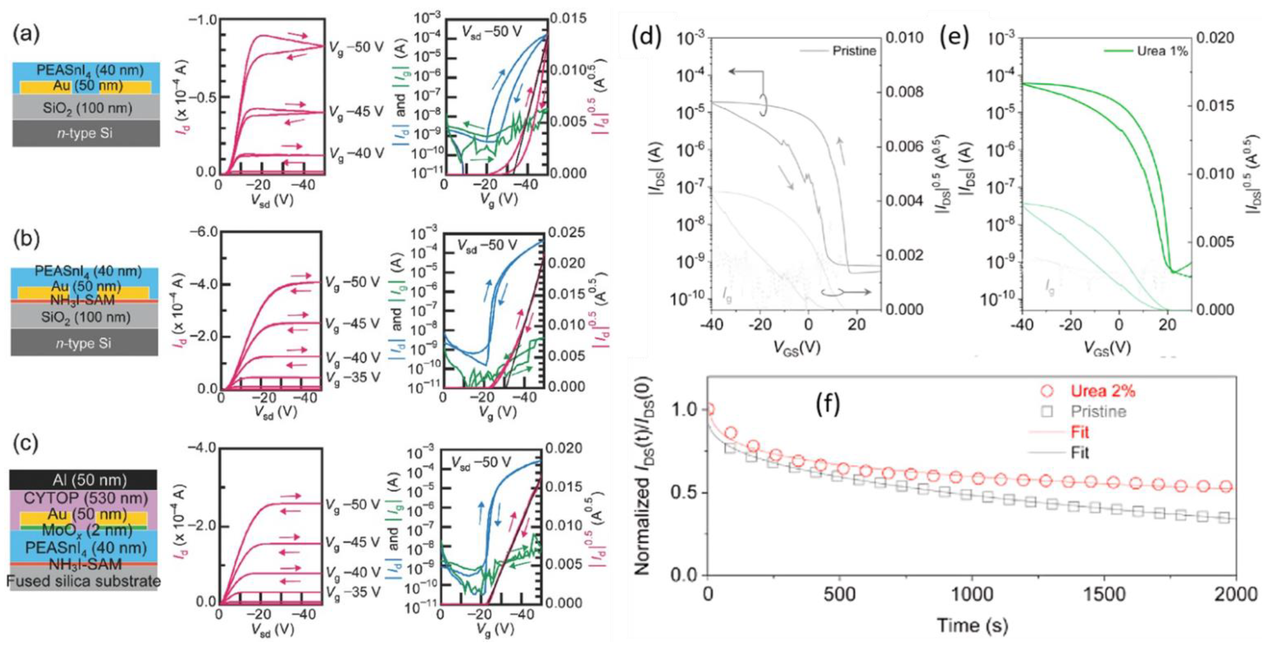
5.1. Hysteresis in the Transfer Curves of the PFETs
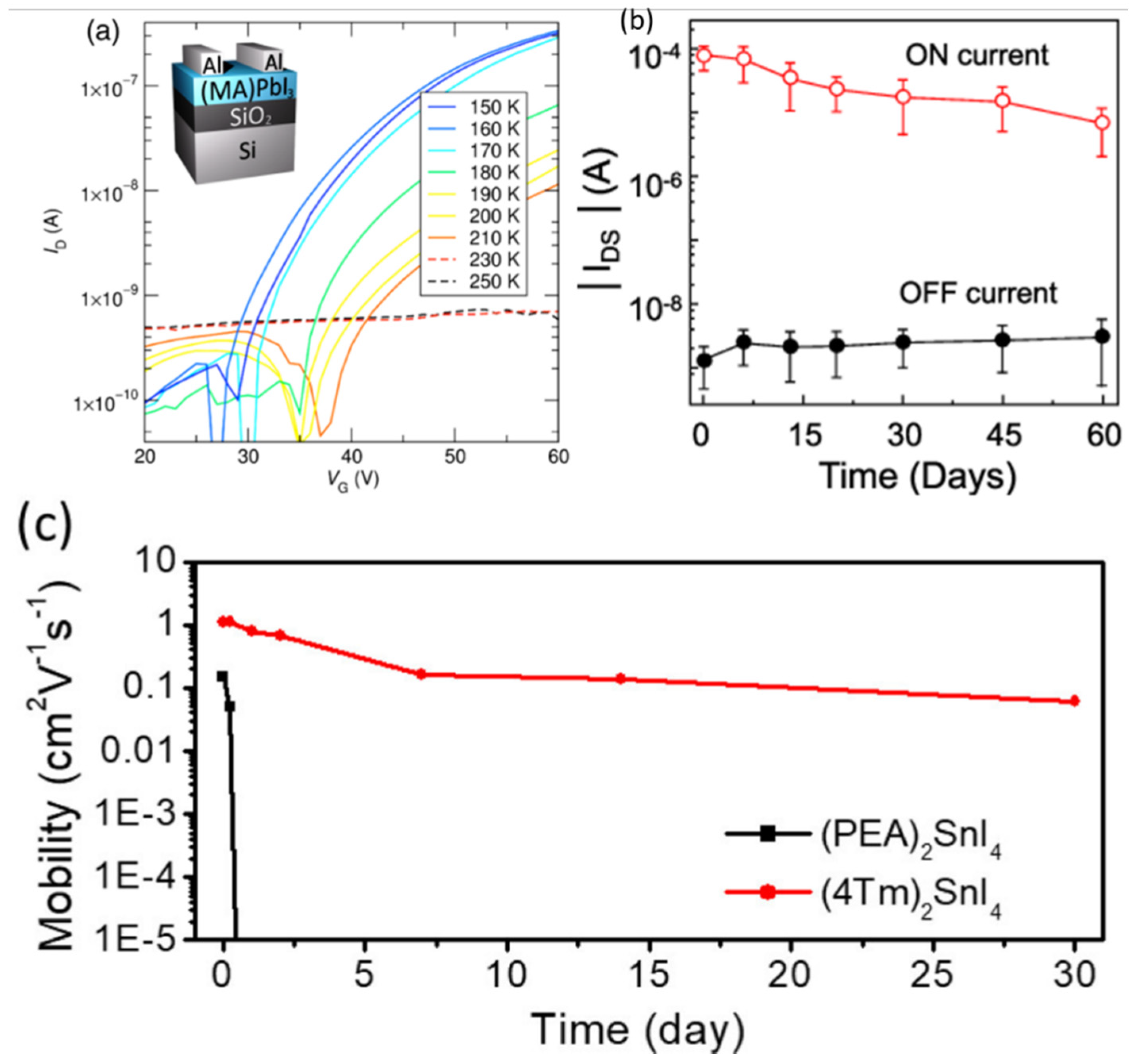
5.2. Operational and Chemical Stability
5.3. Potential of Perovskite FETs and Future Scope
6. Conclusions
Author Contributions
Funding
Conflicts of Interest
References
- Deschler, F.; Neher, D.; Schmidt-Mende, L. Perovskite semiconductors for next generation optoelectronic applications. APL Mater. 2019, 7, 7–10. [Google Scholar] [CrossRef] [Green Version]
- Fu, Y.; Zhu, H.; Chen, J.; Hautzinger, M.P.; Zhu, X.Y.; Jin, S. Metal halide perovskite nanostructures for optoelectronic applications and the study of physical properties. Nat. Rev. Mater. 2019, 4, 169–188. [Google Scholar] [CrossRef]
- Rhee, S.; An, K.; Kang, K.T. Recent advances and challenges in halide perovskite crystals in optoelectronic devices from solar cells to other applications. Crystals 2021, 11, 39. [Google Scholar] [CrossRef]
- Rezaee, E.; Kutsarov, D.; Li, B.; Bi, J.; Silva, S.R.P. OPEN A route towards the fabrication of large-scale and high-quality perovskite films for optoelectronic devices. Sci. Rep. 2022, 12, 7411. [Google Scholar] [CrossRef]
- Hao, J.; Xiao, X. Recent Development of Optoelectronic Application Based on Metal Halide Perovskite Nanocrystals. Front. Chem. 2022, 9, 822106. [Google Scholar] [CrossRef]
- Ouedraogo, N.A.N.; Chen, Y.; Xiao, Y.Y.; Meng, Q.; Han, C.B.; Yan, H.; Zhang, Y. Stability of all-inorganic perovskite solar cells. Nano Energy 2020, 67, 104249. [Google Scholar] [CrossRef]
- Li, Z.; Klein, T.R.; Kim, D.H.; Yang, M.; Berry, J.J.; Van Hest, M.F.A.M.; Zhu, K. Scalable fabrication of perovskite solar cells. Nat. Rev. Mater. 2018, 3, 18017. [Google Scholar] [CrossRef]
- Wang, S.; Yousefi Amin, A.A.; Wu, L.; Cao, M.; Zhang, Q.; Ameri, T. Perovskite Nanocrystals: Synthesis, Stability, and Optoelectronic Applications. Small Struct. 2021, 2, 2000124. [Google Scholar] [CrossRef]
- Braga, J.P.; De Lima, G.R.; Gozzi, G.; Santos, L.F. Electrical Characterization of Thin-Film Transistors Based on Solution-Processed Metal Oxides. Des. Simul. Constr. Field Eff. Transistors 2018. [Google Scholar] [CrossRef] [Green Version]
- Zhu, H.; Liu, A.; Noh, Y.Y. Recent progress on metal halide perovskite field-effect transistors. J. Inf. Disp. 2021, 22, 257–268. [Google Scholar] [CrossRef]
- Paulus, F.; Tyznik, C.; Jurchescu, O.D.; Vaynzof, Y. Switched-On: Progress, Challenges, and Opportunities in Metal Halide Perovskite Transistors. Adv. Funct. Mater. 2021, 31, 2101029. [Google Scholar] [CrossRef]
- Kojima, A.; Teshima, K.; Shirai, Y.; Miyasaka, T. Organometal halide perovskites as visible-light sensitizers for photovoltaic cells. J. Am. Chem. Soc. 2009, 131, 6050–6051. [Google Scholar] [CrossRef] [PubMed]
- Mei, Y.; Zhang, C.; Vardeny, Z.V.; Jurchescu, O.D. Electrostatic gating of hybrid halide perovskite field-effect transistors: Balanced ambipolar transport at room-temperature. MRS Commun. 2015, 5, 297–301. [Google Scholar] [CrossRef] [Green Version]
- Mathews, S.; Ramesh, R.; Venkatesan, T.; Benedetto, J. Ferroelectric field effect transistor based on epitaxial perovskite heterostructures. Science 1997, 276, 238–240. [Google Scholar] [CrossRef] [PubMed]
- Kagan, C.R.; Mitzi, D.B.; Dimitrakopoulos, C.D. Organic-inorganic hybrid materials as semiconducting channels in thin-film field-effect transistors. Science 1999, 286, 945–947. [Google Scholar] [CrossRef] [PubMed]
- Mitzi, D.B.; Dimitrakopoulos, C.D.; Kosbar, L.L. Structurally tailored organic-inorganic perovskites: Optical properties and solution-processed channel materials for thin-film transistors. Chem. Mater. 2001, 13, 3728–3740. [Google Scholar] [CrossRef]
- Motta, C.; El-Mellouhi, F.; Sanvito, S. Charge carrier mobility in hybrid halide perovskites. Sci. Rep. 2015, 5, 12746. [Google Scholar] [CrossRef]
- Miao, J.; Zhang, F. Recent progress on highly sensitive perovskite photodetectors. J. Mater. Chem. C 2019, 7, 1741–1791. [Google Scholar] [CrossRef]
- Wang, J.; Liu, F.; Wang, G.; Wang, L.; Jiang, C. Novel organic-perovskite hybrid structure forward photo field effect transistor. Org. Electron. 2016, 38, 158–163. [Google Scholar] [CrossRef]
- Chin, X.Y.; Cortecchia, D.; Yin, J.; Bruno, A.; Soci, C. Lead iodide perovskite light-emitting field-effect transistor. Nat. Commun. 2015, 6, 7383. [Google Scholar] [CrossRef]
- Wu, T.; Pisula, W.; Rashid, M.Y.A.; Gao, P. Application of Perovskite-Structured Materials in Field-Effect Transistors. Adv. Electron. Mater. 2019, 5, 1900444. [Google Scholar] [CrossRef]
- Zhang, C.; Kuang, D.B.; Wu, W.Q. A Review of Diverse Halide Perovskite Morphologies for Efficient Optoelectronic Applications. Small Methods 2020, 4, 1900662. [Google Scholar] [CrossRef]
- You, I.; Noh, Y.Y. Toward high-performance p-type, tin-based perovskite thin film transistors. Appl. Phys. Lett. 2021, 118, 250501. [Google Scholar] [CrossRef]
- Liu, Y.; Chen, P.A.; Hu, Y. Recent developments in fabrication and performance of metal halide perovskite field-effect transistors. J. Mater. Chem. C 2020, 8, 16691–16715. [Google Scholar] [CrossRef]
- Liu, X.; Yu, D.; Song, X.; Zeng, H. Metal Halide Perovskites: Synthesis, Ion Migration, and Application in Field-Effect Transistors. Small 2018, 14, 1801460. [Google Scholar] [CrossRef]
- Lin, Y.H.; Pattanasattayavong, P.; Anthopoulos, T.D. Metal-Halide Perovskite Transistors for Printed Electronics: Challenges and Opportunities. Adv. Mater. 2017, 29, 1702838. [Google Scholar] [CrossRef] [PubMed]
- Xie, C.; Liu, C.K.; Loi, H.L.; Yan, F. Perovskite-Based Phototransistors and Hybrid Photodetectors. Adv. Funct. Mater. 2020, 30, 1903907. [Google Scholar] [CrossRef]
- Zhou, J.; Huang, J. Photodetectors Based on Organic–Inorganic Hybrid Lead Halide Perovskites. Adv. Sci. 2018, 5, 1700256. [Google Scholar] [CrossRef]
- Stylianakis, M.M.; Maksudov, T.; Panagiotopoulos, A.; Kakavelakis, G.; Petridis, K. Inorganic and hybrid perovskite based laser devices: A Review. Materials 2019, 16, 859. [Google Scholar] [CrossRef] [PubMed] [Green Version]
- Kakavelakis, G.; Gedda, M.; Panagiotopoulos, A.; Kymakis, E.; Anthopoulos, T.D.; Petridis, K. Metal Halide Perovskites for High-Energy Radiation Detection. Adv. Sci. 2020, 7, 2002098. [Google Scholar] [CrossRef]
- Gao, W.; Zhu, Y.; Wang, Y.; Yuan, G.; Liu, J.M. A review of flexible perovskite oxide ferroelectric films and their application. J. Mater. 2020, 6, 1–16. [Google Scholar] [CrossRef]
- Cai, W.; Wang, H.; Zang, Z.; Ding, L. 2D perovskites for field-effect transistors. Sci. Bull. 2021, 66, 648–650. [Google Scholar] [CrossRef]
- Jena, A.K.; Kulkarni, A.; Miyasaka, T. Halide Perovskite Photovoltaics: Background, Status, and Future Prospects. Chem. Rev. 2019, 119, 3036–3103. [Google Scholar] [CrossRef] [PubMed]
- Schmidt, L.C.; Pertegás, A.; González-Carrero, S.; Malinkiewicz, O.; Agouram, S.; Mínguez Espallargas, G.; Bolink, H.J.; Galian, R.E.; Pérez-Prieto, J. Nontemplate synthesis of CH3NH3PbBr3 perovskite nanoparticles. J. Am. Chem. Soc. 2014, 136, 850–853. [Google Scholar] [CrossRef] [PubMed]
- Horváth, E.; Spina, M.; Szekrényes, Z.; Kamarás, K.; Gaal, R.; Gachet, D.; Forró, L. Nanowires of Methylammonium Lead Iodide (CH3NH3PbI3) prepared by low temperature solution-mediated crystallization. Nano Lett. 2014, 14, 6761–6766. [Google Scholar] [CrossRef] [Green Version]
- Li, P.; Chen, Y.; Yang, T.; Wang, Z.; Lin, H.; Xu, Y.; Li, L.; Mu, H.; Shivananju, B.N.; Zhang, Y.; et al. Two-Dimensional CH3NH3PbI3 Perovskite Nanosheets for Ultrafast Pulsed Fiber Lasers. ACS Appl. Mater. Interfaces 2017, 9, 12759–12765. [Google Scholar] [CrossRef]
- Dang, Y.; Liu, Y.; Sun, Y.; Yuan, D.; Liu, X.; Lu, W.; Liu, G.; Xia, H.; Tao, X. Bulk crystal growth of hybrid perovskite material CH3NH3PbI3. CrystEngComm 2015, 17, 665–670. [Google Scholar] [CrossRef]
- Hamukwaya, S.L.; Hao, H.; Zhao, Z.; Dong, J.; Zhong, T.; Xing, J.; Hao, L.; Mashingaidze, M.M. A Review of Recent Developments in Preparation Methods for Large-Area Perovskite Solar Cells. Coatings 2022, 12, 252. [Google Scholar] [CrossRef]
- Cheng, C.; Zhu, C.; Huang, B.; Zhang, H.; Zhang, H.; Chen, R.; Pei, W.; Chen, Q.; Chen, H. Processing Halide Perovskite Materials with Semiconductor Technology. Adv. Mater. Technol. 2019, 4, 1800729. [Google Scholar] [CrossRef]
- Quan, L.N.; Rand, B.P.; Friend, R.H.; Mhaisalkar, S.G.; Lee, T.W.; Sargent, E.H. Perovskites for Next-Generation Optical Sources. Chem. Rev. 2019, 119, 7444–7477. [Google Scholar] [CrossRef]
- Kang, J.; Cho, J.H. Organic-inorganic hybrid perovskite electronics. Phys. Chem. Chem. Phys. 2020, 22, 13347–13357. [Google Scholar] [CrossRef] [PubMed]
- Wu, Y.; Li, J.; Xu, J.; Du, Y.; Huang, L.; Ni, J.; Cai, H.; Zhang, J. Organic-inorganic hybrid CH3NH3PbI3 perovskite materials as channels in thin-film field-effect transistors. RSC Adv. 2016, 6, 16243–16249. [Google Scholar] [CrossRef]
- Pistor, P.; Ruiz, A.; Cabot, A.; Izquierdo-Roca, V. Advanced Raman Spectroscopy of Methylammonium Lead Iodide: Development of a Non-destructive Characterisation Methodology. Sci. Rep. 2016, 6, 35973. [Google Scholar] [CrossRef] [PubMed]
- Nakada, K.; Matsumoto, Y.; Shimoi, Y.; Yamada, K.; Furukawa, Y. Temperature-dependent evolution of Raman spectra of methylammonium lead halide perovskites, CH3NH3PbX3 (X = I, Br). Molecules 2019, 24, 626. [Google Scholar] [CrossRef] [PubMed] [Green Version]
- Egger, D.A.; Rappe, A.M.; Kronik, L. Hybrid Organic-Inorganic Perovskites on the Move. Acc. Chem. Res. 2016, 49, 573–581. [Google Scholar] [CrossRef] [PubMed]
- Ünlü, F.; Jung, E.; Haddad, J.; Kulkarni, A.; Öz, S.; Choi, H.; Fischer, T.; Chakraborty, S.; Kirchartz, T.; Mathur, S. Understanding the interplay of stability and efficiency in A-site engineered lead halide perovskites. APL Mater. 2020, 8, 070901. [Google Scholar] [CrossRef]
- Ananthakumar, S.; Moorthy Babu, S. Progress on synthesis and applications of hybrid perovskite semiconductor nanomaterials—A review. Synth. Met. 2018, 246, 64–95. [Google Scholar] [CrossRef]
- Senocrate, A.; Kim, G.Y.; Grätzel, M.; Maier, J. Thermochemical Stability of Hybrid Halide Perovskites. ACS Energy Lett. 2019, 4, 2859–2870. [Google Scholar] [CrossRef] [Green Version]
- Deretzis, I.; Smecca, E.; Mannino, G.; La Magna, A.; Miyasaka, T.; Alberti, A. Stability and Degradation in Hybrid Perovskites: Is the Glass Half-Empty or Half-Full? J. Phys. Chem. Lett. 2018, 9, 3000–3007. [Google Scholar] [CrossRef]
- López, C.A.; Abia, C.; Rodrigues, J.E.; Serrano-Sánchez, F.; Nemes, N.M.; Martínez, J.L.; Fernandez-Díaz, M.T.; Biškup, N.; Alvarez-Galván, C.; Carrascoso, F.; et al. Enhanced stability in CH3NH3PbI3 hybrid perovskite from mechano-chemical synthesis: Structural, microstructural and optoelectronic characterization. Sci. Rep. 2020, 10, 11228. [Google Scholar] [CrossRef]
- Xia, C.Q.; Peng, J.; Poncé, S.; Patel, J.B.; Wright, A.D.; Crothers, T.W.; Uller Rothmann, M.; Borchert, J.; Milot, R.L.; Kraus, H.; et al. Limits to Electrical Mobility in Lead-Halide Perovskite Semiconductors. J. Phys. Chem. Lett. 2021, 12, 3607–3617. [Google Scholar] [CrossRef] [PubMed]
- Futscher, M.H.; Milić, J.V. Mixed Conductivity of Hybrid Halide Perovskites: Emerging Opportunities and Challenges. Front. Energy Res. 2021, 9, 629074. [Google Scholar] [CrossRef]
- Assirey, E.A.R. Perovskite synthesis, properties and their related biochemical and industrial application. Saudi Pharm. J. 2019, 27, 817–829. [Google Scholar] [CrossRef] [PubMed]
- Cao, L.; Liu, X.; Li, Y.; Li, X.; Du, L.; Chen, S.; Zhao, S.; Wang, C. Recent progress in all-inorganic metal halide nanostructured perovskites: Materials design, optical properties, and application. Front. Phys. 2021, 16, 33201. [Google Scholar] [CrossRef]
- Gaulding, E.A.; Hao, J.; Kang, H.S.; Miller, E.M.; Habisreutinger, S.N.; Zhao, Q.; Hazarika, A.; Sercel, P.C.; Luther, J.M.; Blackburn, J.L. Conductivity Tuning via Doping with Electron Donating and Withdrawing Molecules in Perovskite CsPbI3 Nanocrystal Films. Adv. Mater. 2019, 31, 1902250. [Google Scholar] [CrossRef] [PubMed] [Green Version]
- Chen, W.; Li, X.; Li, Y.; Li, Y. A review: Crystal growth for high-performance all-inorganic perovskite solar cells. Energy Environ. Sci. 2020, 13, 1971–1996. [Google Scholar] [CrossRef]
- Yang, H.; Zhang, Y.; Pan, J.; Yin, J.; Bakr, O.M.; Mohammed, O.F. Room-Temperature Engineering of All-Inorganic Perovskite Nanocrsytals with Different Dimensionalities. Chem. Mater. 2017, 29, 8978–8982. [Google Scholar] [CrossRef]
- Cho, H.; Kim, Y.H.; Wolf, C.; Lee, H.D.; Lee, T.W. Improving the Stability of Metal Halide Perovskite Materials and Light-Emitting Diodes. Adv. Mater. 2018, 30, 1704587. [Google Scholar] [CrossRef]
- Chu, L.; Ahmad, W.; Liu, W.; Yang, J.; Zhang, R.; Sun, Y.; Yang, J.; Li, X. Lead-Free Halide Double Perovskite Materials: A New Superstar toward Green and Stable Optoelectronic Applications. Nano-Micro Lett. 2019, 11, 16. [Google Scholar] [CrossRef] [Green Version]
- Ahmad, S.; Kanaujia, P.K.; Beeson, H.J.; Abate, A.; Deschler, F.; Credgington, D.; Steiner, U.; Prakash, G.V.; Baumberg, J.J. Strong Photocurrent from Two-Dimensional Excitons in Solution-Processed Stacked Perovskite Semiconductor Sheets. ACS Appl. Mater. Interfaces 2015, 7, 25227–25236. [Google Scholar] [CrossRef]
- Mir, W.J.; Sheikh, T.; Arfin, H.; Xia, Z.; Nag, A. Lanthanide doping in metal halide perovskite nanocrystals: Spectral shifting, quantum cutting and optoelectronic applications. NPG Asia Mater. 2020, 12, 9. [Google Scholar] [CrossRef]
- Pedesseau, L.; Sapori, D.; Traore, B.; Robles, R.; Fang, H.H.; Loi, M.A.; Tsai, H.; Nie, W.; Blancon, J.C.; Neukirch, A.; et al. Advances and Promises of Layered Halide Hybrid Perovskite Semiconductors. ACS Nano 2016, 10, 9776–9786. [Google Scholar] [CrossRef] [PubMed] [Green Version]
- Herz, L.M. Charge-Carrier Mobilities in Metal Halide Perovskites: Fundamental Mechanisms and Limits. ACS Energy Lett. 2017, 2, 1539–1548. [Google Scholar] [CrossRef]
- Gao, Y.; Wei, Z.; Hsu, S.N.; Boudouris, B.W.; Dou, L. Two-dimensional halide perovskites featuring semiconducting organic building blocks. Mater. Chem. Front. 2020, 4, 3400–3418. [Google Scholar] [CrossRef]
- Fakharuddin, A.; Shabbir, U.; Qiu, W.; Iqbal, T.; Sultan, M.; Heremans, P.; Schmidt-Mende, L. Inorganic and Layered Perovskites for Optoelectronic Devices. Adv. Mater. 2019, 31, 1807095. [Google Scholar] [CrossRef]
- Zaumseil, J.; Sirringhaus, H. Electron and ambipolar transport in organic field-effect transistors. Chem. Rev. 2007, 107, 1296–1323. [Google Scholar] [CrossRef]
- Kim, M.; Ryu, S.U.; Park, S.A.; Choi, K.; Kim, T.; Chung, D.; Park, T. Donor–Acceptor-Conjugated Polymer for High-Performance Organic Field-Effect Transistors: A Progress Report. Adv. Funct. Mater. 2020, 30, 1904545. [Google Scholar] [CrossRef]
- Yu, W.; Li, F.; Yu, L.; Niazi, M.R.; Zou, Y.; Corzo, D.; Basu, A.; Ma, C.; Dey, S.; Tietze, M.L.; et al. Single crystal hybrid perovskite field-effect transistors. Nat. Commun. 2018, 9, 5354. [Google Scholar] [CrossRef] [Green Version]
- Senanayak, S.P.; Abdi-Jalebi, M.; Kamboj, V.S.; Carey, R.; Shivanna, R.; Tian, T.; Schweicher, G.; Wang, J.; Giesbrecht, N.; Di Nuzzo, D.; et al. A general approach for hysteresis-free, operationally stable metal halide perovskite field-effect transistors. Sci. Adv. 2020, 6, 1–13. [Google Scholar] [CrossRef] [Green Version]
- Lee, B.Y.; Minami, T.; Kanashima, T.; Okuyama, M. Fabrication and characterization of ferroelectric gate field-effect transistor memory based on ferroelectric-insulator interface conduction. Jpn. J. Appl. Phys. Part 1 Regul. Pap. Short Notes Rev. Pap. 2006, 45, 8608–8610. [Google Scholar] [CrossRef]
- Cheng, J.; Wang, C.; Freeze, C.; Shoron, O.; Combs, N.; Yang, H.; Kalarickal, N.K.; Xia, Z.; Stemmer, S.; Rajan, S.; et al. High-Current Perovskite Oxide BaTiO3/BaSnO3 Heterostructure Field Effect Transistors. IEEE Electron. Device Lett. 2020, 41, 621–624. [Google Scholar] [CrossRef]
- Prew, B.A. Physics of Semiconductor Devices; Wiley-Interscience: Hoboken, NJ, USA, 1975; Volume 26, ISBN 9780470068328. [Google Scholar]
- Matsumura, M.; Nara, Y. High-performance amorphous-silicon field-effect transistors. J. Appl. Phys. 1980, 51, 6443–6444. [Google Scholar] [CrossRef]
- Pfleiderer, H.; Kusian, W. Ambipolar field-effect transistor. Solid State Electron. 1986, 29, 317–319. [Google Scholar] [CrossRef]
- Daus, A.; Roldán-Carmona, C.; Domanski, K.; Knobelspies, S.; Cantarella, G.; Vogt, C.; Grätzel, M.; Nazeeruddin, M.K.; Tröster, G. Metal-Halide Perovskites for Gate Dielectrics in Field-Effect Transistors and Photodetectors Enabled by PMMA Lift-Off Process. Adv. Mater. 2018, 30, 1707412. [Google Scholar] [CrossRef]
- Yusoff, A.R.b.M.; Kim, H.P.; Li, X.; Kim, J.; Jang, J.; Nazeeruddin, M.K. Ambipolar Triple Cation Perovskite Field Effect Transistors and Inverters. Adv. Mater. 2017, 29, 1602940. [Google Scholar] [CrossRef] [PubMed] [Green Version]
- Lin, A.; Patil, N.; Ryu, K.; Badmaev, A.; Gomez De Arco, L.; Zhou, C.; Mitra, S.; Philip Wong, H.S. Threshold voltage and on-off ratio tuning for multiple-tube carbon nanotube FETs. IEEE Trans. Nanotechnol. 2009, 8, 4–9. [Google Scholar] [CrossRef]
- Win, L.L.Y.; Taguchi, D.; Manaka, T. Direct observation of carrier transport in organic-inorganic hybrid perovskite thin film by transient photoluminescence imaging measurement. Jpn. J. Appl. Phys. 2019, 58, SBBG18. [Google Scholar] [CrossRef]
- Zeidell, A.M.; Tyznik, C.; Jennings, L.; Zhang, C.; Lee, H.; Guthold, M.; Vardeny, Z.V.; Jurchescu, O.D. Enhanced Charge Transport in Hybrid Perovskite Field-Effect Transistors via Microstructure Control. Adv. Electron. Mater. 2018, 4, 1800316. [Google Scholar] [CrossRef]
- Choi, H.H.; Cho, K.; Frisbie, C.D.; Sirringhaus, H.; Podzorov, V. Critical assessment of charge mobility extraction in FETs. Nat. Mater. 2017, 17, 2–7. [Google Scholar] [CrossRef]
- Kaifi, M.; Gupta, S.K. Simulation of Perovskite channel Thin Film Transistor. Int. J. Eng. Res. Technol. 2020, 13, 5233–5239. [Google Scholar]
- Liu, J.; Liu, F.; Liu, H.; Hou, R.; Yue, J.; Cai, J.; Peng, Z.; Impundu, J.; Xie, L.; Li, Y.J.; et al. Direct Growth of Perovskite Crystals on Metallic Electrodes for High-Performance Electronic and Optoelectronic Devices. Small 2020, 16, 1906185. [Google Scholar] [CrossRef] [PubMed]
- Zhou, S.; Zhou, G.; Li, Y.; Xu, X.; Hsu, Y.J.; Xu, J.; Zhao, N.; Lu, X. Understanding Charge Transport in All-Inorganic Halide Perovskite Nanocrystal Thin-Film Field Effect Transistors. ACS Energy Lett. 2020, 5, 2614–2623. [Google Scholar] [CrossRef]
- Mitzi, D.B.; Dimitrakopoulos, C.D.; Rosner, J.; Medeiros, D.R.; Xu, Z.; Noyan, C. Hybrid field-effect transistor based on a low-temperature melt-processed channel layer. Adv. Mater. 2002, 14, 1772–1776. [Google Scholar] [CrossRef]
- Matsushima, T.; Fujita, K.; Tsutsui, T. High field-effect hole mobility in organic-inorganic hybrid thin films prepared by vacuum vapor deposition technique. Jpn. J. Appl. Phys. Part 2 Lett. 2004, 43, L1199. [Google Scholar] [CrossRef]
- Matsushima, T.; Yasuda, T.; Fujita, K.; Tsutsui, T. Organic-inorganic field effect transistor with SnI-based perovskite channel layer using vapor phase deposition technique. Org. Field Eff. Transistors II 2003, 5217, 43. [Google Scholar] [CrossRef]
- Matsushima, T.; Fujita, K.; Tsutsui, T. Preparation of conductive organic-inorganic cubic perovskite thin films by dual-source vacuum vapor deposition. Jpn. J. Appl. Phys. Part 1 Regul. Pap. Short Notes Rev. Pap. 2006, 45, 523–525. [Google Scholar] [CrossRef]
- So, K.S.; Wong, K.H. Fabrication and characteriztion of an all-perovskite ferroelectric field effect transistor based on Pb(Zr0.52Ti0.48)O3/LaSrMnO3 heteroepitaxial structures. Ferroelectrics 2001, 260, 213–218. [Google Scholar] [CrossRef]
- Ueno, K.; Inoue, I.H.; Yamada, T.; Akoh, H.; Tokura, Y.; Takagi, H. Field-effect transistor based on KTaO3 perovskite. Appl. Phys. Lett. 2004, 84, 3726–3728. [Google Scholar] [CrossRef] [Green Version]
- Matsushima, T.; Hwang, S.; Sandanayaka, A.S.D.; Qin, C.; Terakawa, S.; Fujihara, T.; Yahiro, M.; Adachi, C. Solution-Processed Organic–Inorganic Perovskite Field-Effect Transistors with High Hole Mobilities. Adv. Mater. 2016, 28, 10275–10281. [Google Scholar] [CrossRef]
- Matsushima, T.; Leyden, M.R.; Fujihara, T.; Qin, C.; Sandanayaka, A.S.D.; Adachi, C. Large metal halide perovskite crystals for field-effect transistor applications. Appl. Phys. Lett. 2019, 115, 120601. [Google Scholar] [CrossRef]
- Kagan, C.R.; Breen, T.L.; Kosbar, L.L. Patterning organic-inorganic thin-film transistors using microcontact printed templates. Appl. Phys. Lett. 2001, 79, 3536–3538. [Google Scholar] [CrossRef]
- Lee, M.M.; Teuscher, J.; Miyasaka, T.; Murakami, T.N.; Snaith, H.J. Efficient hybrid solar cells based on meso-superstructured organometal halide perovskites. Science 2012, 338, 643–647. [Google Scholar] [CrossRef] [PubMed] [Green Version]
- Labram, J.G.; Fabini, D.H.; Perry, E.E.; Lehner, A.J.; Wang, H.; Glaudell, A.M.; Wu, G.; Evans, H.; Buck, D.; Cotta, R.; et al. Temperature-Dependent Polarization in Field-Effect Transport and Photovoltaic Measurements of Methylammonium Lead Iodide. J. Phys. Chem. Lett. 2015, 6, 3565–3571. [Google Scholar] [CrossRef] [PubMed] [Green Version]
- Stoumpos, C.C.; Malliakas, C.D.; Kanatzidis, M.G. Semiconducting tin and lead iodide perovskites with organic cations: Phase transitions, high mobilities, and near-infrared photoluminescent properties. Inorg. Chem. 2013, 52, 9019–9038. [Google Scholar] [CrossRef] [PubMed]
- Poncé, S.; Schlipf, M.; Giustino, F. Origin of Low Carrier Mobilities in Halide Perovskites. ACS Energy Lett. 2019, 4, 456–463. [Google Scholar] [CrossRef]
- Li, F.; Ma, C.; Wang, H.; Hu, W.; Yu, W.; Sheikh, A.D.; Wu, T. Ambipolar solution-processed hybrid perovskite phototransistors. Nat. Commun. 2015, 6, 8238. [Google Scholar] [CrossRef] [PubMed] [Green Version]
- Li, Y.; Cui, K.; Xu, X.; Chen, J.; Liu, Y.; Wu, J.; Lu, S.; Qin, W.; Wu, X. Understanding the Essential Role of PbI2Films in a High-Performance Lead Halide Perovskite Photodetector. J. Phys. Chem. C 2020, 124, 15107–15114. [Google Scholar] [CrossRef]
- Sun, Y.; Teng, C.; Xie, D.; Qian, L.; Sun, M. Photomodulated Hysteresis Behaviors in Perovskite Phototransistors with Ultra-Low Operating Voltage. J. Phys. Chem. C 2017, 121, 11665–11671. [Google Scholar] [CrossRef]
- Kim, Y.; Park, B. Understanding charge trapping/detrapping at the zinc oxide (ZnO)/MAPbI3 perovskite interface in the dark and under illumination using a ZnO/perovskite/ZnO test platform. Nanoscale 2018, 10, 20377–20383. [Google Scholar] [CrossRef]
- Park, Y.; Park, B. Interfacial energy band bending and carrier trapping at the vacuum-deposited MAPbI3 perovskite/gate dielectric interface. Results Phys. 2018, 11, 302–305. [Google Scholar] [CrossRef]
- Maddalena, F.; Chin, X.Y.; Cortecchia, D.; Bruno, A.; Soci, C. Brightness Enhancement in Pulsed-Operated Perovskite Light-Emitting Transistors. ACS Appl. Mater. Interfaces 2018, 10, 37316–37325. [Google Scholar] [CrossRef] [PubMed]
- Tang, L.; Peng, Y.; Zhou, Z.; Wu, Y.; Xu, J.; Li, J.; Du, Y.; Huang, L.; Cai, H.; Ni, J.; et al. High-performance organic–inorganic hybrid perovskite thin-film field-effect transistors. Appl. Phys. A Mater. Sci. Process. 2018, 124, 624. [Google Scholar] [CrossRef]
- Yu, H.; Cheng, Y.; Shin, D.; Tsang, S.W.; So, F. Vertical Organic–Inorganic Hybrid Perovskite Schottky Junction Transistors. Adv. Electron. Mater. 2018, 4, 1800039. [Google Scholar] [CrossRef]
- Liu, C.K.; Tai, Q.; Wang, N.; Tang, G.; Loi, H.L.; Yan, F. Sn-Based Perovskite for Highly Sensitive Photodetectors. Adv. Sci. 2019, 6, 1900751. [Google Scholar] [CrossRef] [Green Version]
- Bowman, A.R.; Klug, M.T.; Doherty, T.A.S.; Farrar, M.D.; Senanayak, S.P.; Wenger, B.; Divitini, G.; Booker, E.P.; Andaji-Garmaroudi, Z.; Macpherson, S.; et al. Microsecond Carrier Lifetimes, Controlled p-Doping, and Enhanced Air Stability in Low-Bandgap Metal Halide Perovskites. ACS Energy Lett. 2019, 4, 2301–2307. [Google Scholar] [CrossRef]
- Hong, Z.; Zhao, J.; Huang, K.; Cheng, B.; Xiao, Y.; Lei, S. Controllable switching properties in an individual CH3NH3PbI3 micro/nanowire-based transistor for gate voltage and illumination dual-driving non-volatile memory. J. Mater. Chem. C 2019, 7, 4259–4266. [Google Scholar] [CrossRef]
- Wang, J.; Senanayak, S.P.; Liu, J.; Hu, Y.; Shi, Y.; Li, Z.; Zhang, C.; Yang, B.; Jiang, L.; Di, D.; et al. Investigation of Electrode Electrochemical Reactions in CH3NH3PbBr3 Perovskite Single-Crystal Field-Effect Transistors. Adv. Mater. 2019, 31, 1902618. [Google Scholar] [CrossRef]
- Kim, Y.; Park, B. Interfacial charge transport in MAPbI 3 perovskite on ZnO. Results Phys. 2019, 13, 18–21. [Google Scholar] [CrossRef]
- Agrawal, K.; Gupta, V.; Srivastava, R.; Rajput, S.S. Perovskite Resonant Tunneling FET with Sequential Negative Differential Resistance Peaks. ACS Appl. Electron. Mater. 2019, 1, 735–744. [Google Scholar] [CrossRef]
- Chen, P.A.; Guo, J.; Nouri, M.; Tao, Q.; Li, Z.; Li, Q.; Du, L.; Chen, H.; Dong, Z.; Chang, L.; et al. Microfluidic solution-processed organic and perovskite nanowires fabricated for field-effect transistors and photodetectors. J. Mater. Chem. C 2020, 8, 2353–2362. [Google Scholar] [CrossRef]
- Rastogi, P.; Chu, A.; Gréboval, C.; Qu, J.; Noumbé, U.N.; Chee, S.S.; Goyal, M.; Khalili, A.; Xu, X.Z.; Cruguel, H.; et al. Pushing Absorption of Perovskite Nanocrystals into the Infrared. Nano Lett. 2020, 20, 3999–4006. [Google Scholar] [CrossRef] [PubMed]
- Li, J.; Zhou, Z.; Peng, Y.; Zhang, J.; Guo, N.; Sun, Y. A novel TFT with organic-inorganic hybrid perovskite channel layer. Org. Electron. 2020, 84, 105740. [Google Scholar] [CrossRef]
- McClintock, L.; Xiao, R.; Hou, Y.; Gibson, C.; Travaglini, H.C.; Abramovitch, D.; Tan, L.Z.; Senger, R.T.; Fu, Y.; Jin, S.; et al. Temperature and Gate Dependence of Carrier Diffusion in Single Crystal Methylammonium Lead Iodide Perovskite Microstructures. J. Phys. Chem. Lett. 2020, 11, 1000–1006. [Google Scholar] [CrossRef] [PubMed]
- Canicoba, N.D.; Zagni, N.; Liu, F.; McCuistian, G.; Fernando, K.; Bellezza, H.; Traore, B.; Rogel, R.; Tsai, H.; Le Brizoual, L.; et al. Halide perovskite high-K field effect transistors with dynamically reconfigurable ambipolarity. ACS Mater. Lett. 2019, 1, 633–640. [Google Scholar] [CrossRef] [Green Version]
- Win, L.L.Y.; Taguchi, D.; Manaka, T. Transient carrier visualization of organic-inorganic hybrid perovskite thin films by using time-resolved microscopic second-harmonic generation (TRM-SHG). Org. Electron. 2019, 75, 105416. [Google Scholar] [CrossRef]
- Khorramshahi, F.; Takshi, A. Microfluidic approach for lead halide perovskite flexible phototransistors. Electronics 2020, 9, 1852. [Google Scholar] [CrossRef]
- Zou, Y.; Zou, T.; Zhao, C.; Wang, B.; Xing, J.; Yu, Z.; Cheng, J.; Xin, W.; Yang, J.; Yu, W.; et al. A Highly Sensitive Single Crystal Perovskite–Graphene Hybrid Vertical Photodetector. Small 2020, 16, 2000733. [Google Scholar] [CrossRef] [PubMed]
- Brus, V.V.; Lang, F.; Fengler, S.; Dittrich, T.; Rappich, J.; Nickel, N.H. Doping Effects and Charge-Transfer Dynamics at Hybrid Perovskite/Graphene Interfaces. Adv. Mater. Interfaces 2018, 5, 1800826. [Google Scholar] [CrossRef]
- Kim, H.P.; Vasilopoulou, M.; Ullah, H.; Bibi, S.; Gavim, A.E.X.; Macedo, A.G.; Da Silva, W.J.; Schneider, F.K.; Tahir, A.A.; Teridi, M.A.M.; et al. A hysteresis-free perovskite transistor with exceptional stability through molecular cross-linking and amine-based surface passivation. Nanoscale 2020, 12, 7641–7650. [Google Scholar] [CrossRef]
- Luan, S.Z.; Wang, Y.C.; Liu, Y.T.; Jia, R.X. Effect of depositing PCBM on perovskite-based metal-oxide-semiconductor field effect transistors. Chin. Phys. B 2018, 27, 047208. [Google Scholar] [CrossRef]
- Zhou, Z.; Guo, N.; Peng, Y.; Tang, L.; Zhang, J.; Cai, H.; Ni, J.; Sun, Y.; Li, J. The Effect of Annealing Pressure on Perovskite Films and Its Thin-Film Field-Effect Transistors’ Performance. Phys. Status Solidi Appl. Mater. Sci. 2019, 216, 1900434. [Google Scholar] [CrossRef]
- Shao, S.; Talsma, W.; Pitaro, M.; Dong, J.; Kahmann, S.; Rommens, A.J.; Portale, G.; Loi, M.A. Field-Effect Transistors Based on Formamidinium Tin Triiodide Perovskite. Adv. Funct. Mater. 2021, 31, 2008478. [Google Scholar] [CrossRef]
- Haque, F.; Bukke, R.N.; Mativenga, M. Reduction of hysteresis in hybrid perovskite transistors by solvent-controlled growth. Materials 2021, 14, 2573. [Google Scholar] [CrossRef] [PubMed]
- Hoang, N.T.T.; Haque, F.; Ji, J.; Mativenga, M. Fast-Switching Mixed A-Cation Organic-Inorganic Hybrid Perovskite TFTs. IEEE Electron. Device Lett. 2019, 40, 917–920. [Google Scholar] [CrossRef]
- Habibi, M.; Eslamian, M. Facile and low-cost mechanical techniques for the fabrication of solution-processed polymer and perovskite thin film transistors. J. Phys. Commun. 2018, 2, 075018. [Google Scholar] [CrossRef]
- Pininti, A.R.; Ball, J.M.; Albaqami, M.D.; Petrozza, A.; Caironi, M. Time-Dependent Field Effect in Three-Dimensional Lead-Halide Perovskite Semiconductor Thin Films. ACS Appl. Energy Mater. 2021, 4, 10603–10609. [Google Scholar] [CrossRef]
- Peng, H.; Guo, J.; Chen, G.; Qin, W. Self-powered perovskite CH3NH3PbBr3 field effect transistor with fast response and high sensitivity in sensing. Mater. Today Adv. 2021, 12, 100185. [Google Scholar] [CrossRef]
- Zhou, Y.; Tiwale, N.; Yin, Y.; Subramanian, A.; Rafailovich, M.H.; Nam, C.Y. Effects of polymer grain boundary passivation on organic-inorganic hybrid perovskite field-effect transistors. Appl. Phys. Lett. 2021, 119, 183303. [Google Scholar] [CrossRef]
- Klein, M.; Li, J.; Bruno, A.; Soci, C. Co-Evaporated Perovskite Light-Emitting Transistor Operating at Room Temperature. Adv. Electron. Mater. 2021, 7, 2100403. [Google Scholar] [CrossRef]
- Zhu, H.; Liu, A.; Shim, K.I.; Jung, H.; Zou, T.; Reo, Y.; Kim, H.; Han, J.W.; Chen, Y.; Chu, H.Y.; et al. High-performance hysteresis-free perovskite transistors through anion engineering. Nat. Commun. 2022, 13, 1741. [Google Scholar] [CrossRef]
- Youn, J.; Park, C.J.; Teng, X.; Lee, K.S.; Kim, J.; Joo, J. Energy and charge transfer effects for hybrids of perovskite CsPbBr3 quantum dots on organic semiconducting rubrene nanosheet. Org. Electron. 2019, 65, 243–250. [Google Scholar] [CrossRef]
- Zou, Y.; Li, F.; Zhao, C.; Xing, J.; Yu, Z.; Yu, W.; Guo, C. Anomalous Ambipolar Phototransistors Based on All-Inorganic CsPbBr3 Perovskite at Room Temperature. Adv. Opt. Mater. 2019, 7, 1900676. [Google Scholar] [CrossRef]
- Erodici, M.P.; Pierone, P.J.; Hartono, N.T.P.; Hidalgo, J.; Lai, B.; Buonassisi, T.; Correa-Baena, J.P.; Sher, M.J. Enhanced charge carrier lifetime and mobility as a result of Rb and Cs incorporation in hybrid perovskite. Appl. Phys. Lett. 2021, 118, 063901. [Google Scholar] [CrossRef]
- Wang, Y.; Lv, Z.; Chen, J.; Wang, Z.; Zhou, Y.; Zhou, L.; Chen, X.; Han, S.T. Photonic Synapses Based on Inorganic Perovskite Quantum Dots for Neuromorphic Computing. Adv. Mater. 2018, 30, 1802883. [Google Scholar] [CrossRef] [PubMed]
- Aleshin, A.N.; Shcherbakov, I.P.; Kirilenko, D.A.; Matyushkin, L.B.; Moshnikov, V.A. Light-Emitting Field-Effect Transistors Based on Composite Films of Polyfluorene and CsPbBr 3 Nanocrystals. Phys. Solid State 2019, 61, 256–262. [Google Scholar] [CrossRef]
- Yi, H.T.; Rangan, S.; Tang, B.; Frisbie, C.D.; Bartynski, R.A.; Gartstein, Y.N.; Podzorov, V. Electric-field effect on photoluminescence of lead-halide perovskites. Mater. Today 2019, 28, 31–39. [Google Scholar] [CrossRef]
- Noh, T.; Shin, H.S.; Seo, C.; Kim, J.Y.; Youn, J.; Kim, J.; Lee, K.S.; Joo, J. Significant enhancement of photoresponsive characteristics and mobility of MoS2-based transistors through hybridization with perovskite CsPbBr3 quantum dots. Nano Res. 2019, 12, 405–412. [Google Scholar] [CrossRef]
- Li, Q.; Zhang, Y.; Yu, Y.; Chen, Z.; Jin, L.; Li, Y.; Li, T.; Yang, Y.; Zhao, H.; Li, J.; et al. Light enhanced low-voltage nonvolatile memory based on all-inorganic perovskite quantum dots. Nanotechnology 2019, 30, 37LT01. [Google Scholar] [CrossRef]
- Aleshin, A.N.; Shcherbakov, I.P.; Chikalova-Luzina, O.P.; Matyushkin, L.B.; Ovezov, M.K.; Ershova, A.M.; Trapeznikova, I.N.; Petrov, V.N. Photo- and electroluminescence features of films and field effect transistors based on inorganic perovskite nanocrystals embedded in a polymer matrix. Synth. Met. 2020, 260, 116291. [Google Scholar] [CrossRef]
- Hu, X.; Zhou, H.; Jiang, Z.; Wang, X.; Yuan, S.; Lan, J.; Fu, Y.; Zhang, X.; Zheng, W.; Wang, X.; et al. Direct Vapor Growth of Perovskite CsPbBr3 Nanoplate Electroluminescence Devices. ACS Nano 2017, 11, 9869–9876. [Google Scholar] [CrossRef]
- Meng, Y.; Lan, C.; Li, F.; Yip, S.; Wei, R.; Kang, X.; Bu, X.; Dong, R.; Zhang, H.; Ho, J.C. Direct Vapor-Liquid-Solid Synthesis of All-Inorganic Perovskite Nanowires for High-Performance Electronics and Optoelectronics. ACS Nano 2019, 13, 6060–6070. [Google Scholar] [CrossRef] [PubMed]
- Zhou, S.; Ma, Y.; Zhou, G.; Xu, X.; Qin, M.; Li, Y.; Hsu, Y.J.; Hu, H.; Li, G.; Zhao, N.; et al. Ag-Doped Halide Perovskite Nanocrystals for Tunable Band Structure and Efficient Charge Transport. ACS Energy Lett. 2019, 4, 534–541. [Google Scholar] [CrossRef]
- Jeong, B.; Veith, L.; Smolders, T.J.A.M.; Wolf, M.J.; Asadi, K. Room-Temperature Halide Perovskite Field-Effect Transistors by Ion Transport Mitigation. Adv. Mater. 2021, 33, 2100486. [Google Scholar] [CrossRef]
- Liu, A.; Zhu, H.; Bai, S.; Reo, Y.; Zou, T.; Kim, M.G.; Noh, Y.Y. High-performance inorganic metal halide perovskite transistors. Nat. Electron. 2022, 5, 78–83. [Google Scholar] [CrossRef]
- Li, C.; Yang, J.; Su, F.; Tan, J.; Luo, Y.; Ye, S. Conformational disorder of organic cations tunes the charge carrier mobility in two-dimensional organic-inorganic perovskites. Nat. Commun. 2020, 11, 5481. [Google Scholar] [CrossRef]
- Abiram, G.; Gourji, F.H.; Pitchaiya, S.; Ravirajan, P.; Murugathas, T.; Velauthapillai, D. Air processed Cs2AgBiBr6 lead-free double perovskite high-mobility thin-film field-effect transistors. Sci. Rep. 2022, 12, 2455. [Google Scholar] [CrossRef] [PubMed]
- Li, Z.; Senanayak, S.P.; Dai, L.; Kusch, G.; Shivanna, R.; Zhang, Y.; Pradhan, D.; Ye, J.; Huang, Y.T.; Sirringhaus, H.; et al. Understanding the Role of Grain Boundaries on Charge-Carrier and Ion Transport in Cs2AgBiBr6 Thin Films. Adv. Funct. Mater. 2021, 31, 2104981. [Google Scholar] [CrossRef]
- Li, M.K.; Chen, T.P.; Lin, Y.F.; Raghavan, C.M.; Chen, W.L.; Yang, S.H.; Sankar, R.; Luo, C.W.; Chang, Y.M.; Chen, C.W. Intrinsic Carrier Transport of Phase-Pure Homologous 2D Organolead Halide Hybrid Perovskite Single Crystals. Small 2018, 14, 1803763. [Google Scholar] [CrossRef] [PubMed]
- Zhu, L.; Zhang, H.; Lu, Q.; Wang, Y.; Deng, Z.; Hu, Y.; Lou, Z.; Cui, Q.; Hou, Y.; Teng, F. Synthesis of ultrathin two-dimensional organic-inorganic hybrid perovskite nanosheets for polymer field-effect transistors. J. Mater. Chem. C 2018, 6, 3945–3950. [Google Scholar] [CrossRef]
- Zhu, H.; Liu, A.; Luque, H.L.; Sun, H.; Ji, D.; Noh, Y.Y. Perovskite and conjugated polymer wrapped semiconducting carbon nanotube hybrid films for high-performance transistors and phototransistors. ACS Nano 2019, 13, 3971–3981. [Google Scholar] [CrossRef]
- Zhao, Y.Q.; Ma, Q.R.; Liu, B.; Yu, Z.L.; Yang, J.; Cai, M.Q. Layer-dependent transport and optoelectronic property in two-dimensional perovskite: (PEA)2PbI4. Nanoscale 2018, 10, 8677–8688. [Google Scholar] [CrossRef] [PubMed]
- Wang, H.; Chen, Y.; Lim, E.; Wang, X.; Yuan, S.; Zhang, X.; Lu, H.; Wang, J.; Wu, G.; Lin, T.; et al. High-performance lead-free two-dimensional perovskite photo transistors assisted by ferroelectric dielectrics. J. Mater. Chem. C 2018, 6, 12714–12720. [Google Scholar] [CrossRef]
- Shen, H.; Li, J.; Wang, H.; Ma, J.; Wang, J.; Luo, H.; Li, D. Two-Dimensional Lead-Free Perovskite (C6H5C2H4NH3)2CsSn2I7 with High Hole Mobility. J. Phys. Chem. Lett. 2019, 10, 7–12. [Google Scholar] [CrossRef] [PubMed]
- Matsushima, T.; Mathevet, F.; Heinrich, B.; Terakawa, S.; Fujihara, T.; Qin, C.; Sandanayaka, A.S.D.; Ribierre, J.C.; Adachi, C. N-channel field-effect transistors with an organic-inorganic layered perovskite semiconductor. Appl. Phys. Lett. 2016, 109, 253301. [Google Scholar] [CrossRef]
- Matsushima, T.; Terakawa, S.; Leyden, M.R.; Fujihara, T.; Qin, C.; Adachi, C. Toward air-stable field-effect transistors with a tin iodide-based hybrid perovskite semiconductor. J. Appl. Phys. 2019, 125, 235501. [Google Scholar] [CrossRef]
- Gao, Y.; Wei, Z.; Yoo, P.; Shi, E.; Zeller, M.; Zhu, C.; Liao, P.; Dou, L. Highly Stable Lead-Free Perovskite Field-Effect Transistors Incorporating Linear Π-Conjugated Organic Ligands. J. Am. Chem. Soc. 2019, 141, 15577–15585. [Google Scholar] [CrossRef]
- Zhang, F.; Zhang, H.; Zhu, L.; Qin, L.; Wang, Y.; Hu, Y.; Lou, Z.; Hou, Y.; Teng, F. Two-dimensional organic-inorganic hybrid perovskite field-effect transistors with polymers as bottom-gate dielectrics. J. Mater. Chem. C 2019, 7, 4004–4012. [Google Scholar] [CrossRef]
- Wang, X.; Li, K.; Xu, H.; Ali, N.; Wang, Y.; Shen, Q.; Wu, H. Synthesis of large two-dimensional lead-free bismuth-silver double perovskite microplatelets and their application for field-effect transistors. Chem. Commun. 2020, 56, 7917–7920. [Google Scholar] [CrossRef]
- Zhu, H.; Liu, A.; Shim, K.I.; Hong, J.; Han, J.W.; Noh, Y.Y. High-Performance and Reliable Lead-Free Layered-Perovskite Transistors. Adv. Mater. 2020, 32, 2002717. [Google Scholar] [CrossRef]
- Liu, F.; Wang, L.; Wang, J.; Wang, F.; Chen, Y.; Zhang, S.; Sun, H.; Liu, J.; Wang, G.; Hu, Y.; et al. 2D Ruddlesden–Popper Perovskite Single Crystal Field-Effect Transistors. Adv. Funct. Mater. 2021, 31, 2005662. [Google Scholar] [CrossRef]
- Liu, Y.; Chen, P.-A.; Qiu, X.; Guo, J.; Xia, J.; Wei, H.; Xie, H.; Hou, S.; He, M.; Wang, X.; et al. Doping of Sn-based two-dimensional perovskite semiconductor for high-performance field-effect transistors and thermoelectric devices. iScience 2022, 25, 104109. [Google Scholar] [CrossRef]
- Guo, J.; Liu, Y.; Chen, P.; Qiu, X.; Wei, H.; Xia, J.; Chen, H.; Zeng, Z.; Liao, L.; Hu, Y. Tuning the Electrical Performance of 2D Perovskite Field-Effect Transistors by Forming Organic Semiconductor/Perovskite van der Waals Heterojunctions. Adv. Electron. Mater. 2022, 2200148, 2200148. [Google Scholar] [CrossRef]
- Polavarapu, L.; Nickel, B.; Feldmann, J.; Urban, A.S. Advances in Quantum-Confined Perovskite Nanocrystals for Optoelectronics. Adv. Energy Mater. 2017, 7, 1700267. [Google Scholar] [CrossRef] [Green Version]
- Senanayak, S.P.; Yang, B.; Thomas, T.H.; Giesbrecht, N.; Huang, W.; Gann, E.; Nair, B.; Goedel, K.; Guha, S.; Moya, X.; et al. Understanding charge transport in lead iodide perovskite thin-film field-effect transistors. Sci. Adv. 2017, 3, 1–11. [Google Scholar] [CrossRef] [PubMed] [Green Version]
- Ho, J.C.; Meng, Y.; Lai, Z.; Li, F.; Wang, W.; Yip, S.P.; Quan, Q.; Bu, X.; Wang, F.; Bao, Y.; et al. Perovskite core−shell nanowire transistors: Interfacial transfer doping and surface passivation. ACS Nano 2020, 14, 12749–12760. [Google Scholar] [CrossRef]
- Gómez, A.; Wang, Q.; Goñi, A.R.; Campoy-Quiles, M.; Abate, A.; Akbulatov, A.F.; Tsarev, S.A.; Elshobaki, M.; Luchkin, S.Y.; Zhidkov, I.S.; et al. Highly stable and efficient all-inorganic lead-free perovskite solar cells with native-oxide passivation. Nat. Commun. 2020, 10, 16. [Google Scholar] [CrossRef] [Green Version]
- Chen, Y.; Chu, Y.; Wu, X.; Ou-Yang, W.; Huang, J. High-Performance Inorganic Perovskite Quantum Dot–Organic Semiconductor Hybrid Phototransistors. Adv. Mater. 2017, 29, 1704062. [Google Scholar] [CrossRef] [PubMed]
- Chen, Y.; Wu, X.; Chu, Y.; Zhou, J.; Zhou, B.; Huang, J. Hybrid Field-Effect Transistors and Photodetectors Based on Organic Semiconductor and CsPbI3 Perovskite Nanorods Bilayer Structure. Nano-Micro Lett. 2018, 10, 57. [Google Scholar] [CrossRef] [Green Version]
- Sun, J.; Wu, J.; Tong, X.; Lin, F.; Wang, Y.; Wang, Z.M. Organic/Inorganic Metal Halide Perovskite Optoelectronic Devices beyond Solar Cells. Adv. Sci. 2018, 5, 1700780. [Google Scholar] [CrossRef]
- Dogan, F.; Lin, H.; Guilloux-Viry, M.; Peña, O. Focus on properties and applications of perovskites. Sci. Technol. Adv. Mater. 2015, 16, 020301. [Google Scholar] [CrossRef]
- Dong, Q. Electron-hole diffusion lengths > 175 μm in solution-grown CH3NH3PbI3 single crystals. Science 2015, 347, 967–970. [Google Scholar] [CrossRef] [PubMed] [Green Version]
- Li, D.; Cheng, H.C.; Wang, Y.; Zhao, Z.; Wang, G.; Wu, H.; He, Q.; Huang, Y.; Duan, X. The Effect of Thermal Annealing on Charge Transport in Organolead Halide Perovskite Microplate Field-Effect Transistors. Adv. Mater. 2017, 29, 1601959. [Google Scholar] [CrossRef] [PubMed]
- Zou, X.; Li, Y.; Tang, G.; You, P.; Yan, F. Schottky Barrier-Controlled Black Phosphorus/Perovskite Phototransistors with Ultrahigh Sensitivity and Fast Response. Small 2019, 15, 1901004. [Google Scholar] [CrossRef] [PubMed]
- Zhu, H.; Liu, A.; Zou, T.; Jung, H.; Heo, S.; Noh, Y.Y. A Lewis base and boundary passivation bifunctional additive for high performance lead-free layered-perovskite transistors and phototransistors. Mater. Today Energy 2021, 21, 100722. [Google Scholar] [CrossRef]
- Chen, C.; Zhang, X.; Wu, G.; Li, H.; Chen, H. Visible-Light Ultrasensitive Solution-Prepared Layered Organic–Inorganic Hybrid Perovskite Field-Effect Transistor. Adv. Opt. Mater. 2017, 5, 2–6. [Google Scholar] [CrossRef]
- Xia, H.R.; Li, J.; Sun, W.T.; Peng, L.M. Organohalide lead perovskite based photodetectors with much enhanced performance. Chem. Commun. 2014, 50, 13695–13697. [Google Scholar] [CrossRef]
- Yang, B.; Zhang, F.; Chen, J.; Yang, S.; Xia, X.; Pullerits, T.; Deng, W.; Han, K. Ultrasensitive and Fast All-Inorganic Perovskite-Based Photodetector via Fast Carrier Diffusion. Adv. Mater. 2017, 29, 1703758. [Google Scholar] [CrossRef]
- Du, S.; Li, G.; Cao, X.; Wang, Y.; Lu, H.; Zhang, S.; Liu, C.; Zhou, H. Oxide Semiconductor Phototransistor with Organolead Trihalide Perovskite Light Absorber. Adv. Electron. Mater. 2017, 3, 1600325. [Google Scholar] [CrossRef]
- Qin, L.; Wu, L.; Kattel, B.; Li, C.; Zhang, Y.; Hou, Y.; Wu, J.; Chan, W.L. Using Bulk Heterojunctions and Selective Electron Trapping to Enhance the Responsivity of Perovskite–Graphene Photodetectors. Adv. Funct. Mater. 2017, 27, 1704173. [Google Scholar] [CrossRef]
- Song, J.; Cui, Q.; Li, J.; Xu, J.; Wang, Y.; Xu, L.; Xue, J.; Dong, Y.; Tian, T.; Sun, H.; et al. Ultralarge All-Inorganic Perovskite Bulk Single Crystal for High-Performance Visible–Infrared Dual-Modal Photodetectors. Adv. Opt. Mater. 2017, 5, 1700157. [Google Scholar] [CrossRef]
- Yu, Y.; Zhang, Y.; Song, X.; Zhang, H.; Cao, M.; Che, Y.; Dai, H.; Yang, J.; Zhang, H.; Yao, J. High Performances for Solution-Pocessed 0D–0D Heterojunction Phototransistors. Adv. Opt. Mater. 2017, 5, 1700565. [Google Scholar] [CrossRef]
- Fu, Q.; Wang, X.; Liu, F.; Dong, Y.; Liu, Z.; Zheng, S.; Chaturvedi, A.; Zhou, J.; Hu, P.; Zhu, Z.; et al. Ultrathin Ruddlesden–Popper Perovskite Heterojunction for Sensitive Photodetection. Small 2019, 15, 1902890. [Google Scholar] [CrossRef] [PubMed]
- Liu, T.; Tang, W.; Luong, S.; Fenwick, O. High charge carrier mobility in solution processed one-dimensional lead halide perovskite single crystals and their application as photodetectors. Nanoscale 2020, 12, 9688–9695. [Google Scholar] [CrossRef] [PubMed]
- Zhou, F.; Abdelwahab, I.; Leng, K.; Loh, K.P.; Ji, W. 2D Perovskites with Giant Excitonic Optical Nonlinearities for High-Performance Sub-Bandgap Photodetection. Adv. Mater. 2019, 31, 1904155. [Google Scholar] [CrossRef] [PubMed]
- D’Innocenzo, V.; Srimath Kandada, A.R.; De Bastiani, M.; Gandini, M.; Petrozza, A. Tuning the light emission properties by band gap engineering in hybrid lead halide perovskite. J. Am. Chem. Soc. 2014, 136, 17730–17733. [Google Scholar] [CrossRef]
- Kim, H.; Zhao, L.; Price, J.S.; Grede, A.J.; Roh, K.; Brigeman, A.N.; Lopez, M.; Rand, B.P.; Giebink, N.C. Hybrid perovskite light emitting diodes under intense electrical excitation. Nat. Commun. 2018, 9, 4893. [Google Scholar] [CrossRef] [PubMed]
- Chaudhry, M.U.; Wang, N.; Tetzner, K.; Seitkhan, A.; Miao, Y.; Sun, Y.; Petty, M.C.; Anthopoulos, T.D.; Wang, J.; Bradley, D.D.C. Light-Emitting Transistors Based on Solution-Processed Heterostructures of Self-Organized Multiple-Quantum-Well Perovskite and Metal-Oxide Semiconductors. Adv. Electron. Mater. 2019, 5, 1800985. [Google Scholar] [CrossRef]
- Lin, E.L.; Posadas, A.B.; Zheng, L.; Wu, H.W.; Chen, P.-Y.; Coffey, B.M.; Lai, K.; Demkov, A.A.; Smith, D.J.; Ekerdt, J.G. Epitaxial integration of ferroelectric and conductive perovskites on silicon. J. Vac. Sci. Technol. A 2020, 38, 022403. [Google Scholar] [CrossRef]
- Chen, K.W.; Chang, S.J.; Tang, E.Y.T.; Lin, C.P.; Hou, T.H.; Chen, C.H.; Tseng, Y.C. Pulse-Mediated Electronic Tuning of the MoS2-Perovskite Ferroelectric Field Effect Transistors. ACS Appl. Electron. Mater. 2020, 2, 3843–3852. [Google Scholar] [CrossRef]
- Chen, Q.; De Marco, N.; Yang, Y.; Song, T.B.; Chen, C.C.; Zhao, H.; Hong, Z.; Zhou, H.; Yang, Y. Under the spotlight: The organic-inorganic hybrid halide perovskite for optoelectronic applications. Nano Today 2015, 10, 355–396. [Google Scholar] [CrossRef] [Green Version]
- Gourji, F.H.; Velauthapillai, D. A review on Cs-based Pb-free double halide perovskites: From theoretical and experimental studies to doping and applications. Molecules 2021, 26, 2010. [Google Scholar] [CrossRef]
- Yao, Z.; Zhao, W.; Liu, S. Stability of the CsPbI3perovskite: From fundamentals to improvements. J. Mater. Chem. A 2021, 9, 11124–11144. [Google Scholar] [CrossRef]
- Chen, M.; Dong, Q.; Eickemeyer, F.T.; Liu, Y.; Dai, Z.; Carl, A.D.; Bahrami, B.; Chowdhury, A.H.; Grimm, R.L.; Shi, Y.; et al. High-Performance Lead-Free Solar Cells Based on Tin-Halide Perovskite Thin Films Functionalized by a Divalent Organic Cation. ACS Energy Lett. 2020, 5, 2223–2230. [Google Scholar] [CrossRef]
- Niu, G.; Guo, X.; Wang, L. Review of recent progress in chemical stability of perovskite solar cells. J. Mater. Chem. A 2015, 3, 8970–8980. [Google Scholar] [CrossRef]
- Jana, S.; Carlos, E.; Panigrahi, S.; Martins, R.; Fortunato, E. Toward stable solution-processed high-mobility P-type thin film transistors based on halide perovskites. ACS Nano 2020, 14, 14790–14797. [Google Scholar] [CrossRef]
- Jeong, B.; Gkoupidenis, P.; Asadi, K. Solution-Processed Perovskite Field-Effect Transistor Artificial Synapses. Adv. Mater. 2021, 33, 2104034. [Google Scholar] [CrossRef] [PubMed]

| Perovskite Semiconductor | Substrate | Source/Drain | Insulator | Device Structures | μe/μh [cm2 V−1s−1] | Ion/Off | VTH [V] | Ref |
|---|---|---|---|---|---|---|---|---|
| (PEA)2SnI4 | Si | Pd | SiO2 | BGBC | 0.62 | 104 | −30 | [15] |
| (2-PEA)2SnI4 (3-PEA)2SnI4 (4-PEA)2SnI4 | Si | Au | SiO2 | BGBC | 0.24 0.51 0.48 | [16] | ||
| (PEA)2SnI4 | Si | Pd | SiO2 | BGBC | 0.1–0.5 | 104−105 | [92] | |
| (3-MeOPEA)2SnI4 (4-MeOPEA)2SnI4 | Si | SiO2/Polyamide | BGBC | 2.6 1.3 | 106 104 | [84] | ||
| (PEA)2SnI4 | Si | SiO2 | BGBC | 0.28 | 105 | −3.2 | [83] | |
| KTaO3 | Au | Al2O3 | BGTC | 0.4 | 105 | [89] | ||
| (PEA)2SnI4 | Si | Au | SiO2 | BGTC | 0.78 | 4.2 × 10⁵ | −1.7 | [85] |
| MASnI3 | Si | Au/Pt | SiO2 | BGTC | 0.004 | 103 | −7.2 | [87] |
| PZT | Si | Pt | HfO2 | TGBC | 106 | [70] | ||
| PZT | LaAlO3 | La2−XSrXCuO4 | LCMO | TGTC | [14] |
| Perovskite Channel | Substrate | Source Drain | Insulator | Device Structures | μh/μe [cm2 V−1s−1] | Ion/Off | VTH | Ref |
|---|---|---|---|---|---|---|---|---|
| MAPbI3 MAPbI3−XCX | Si | Au | SiO2 | BGTC | 0.18 (0.17) 1.24 (1.01) | 104 | 20, −5 | [97] |
| (MAPbI3)X(MAPbBr3)1−X | Glass | Au/Cr | Cytop | TGBC | 21.36 (49.32) | [98] | ||
| MAPbI3 | Si | Au | HfO2 | BGBC | 1.05 | 104 | −1 | [99] |
| MAPbI3 | Si | ZnO | SiO2 | BGBC | [100] | |||
| MAPbI3 | Si | Au, Ti | SiO2 | BGBC | [101] | |||
| MAPbI3 | Si | Au | SiO2 | BGTC | 0.025 (0.11) | [102] | ||
| MAPbI3 | Si | Au Au/MoOX | SiO2 | BGTC | 3.55 7.47 | 105 | [103] | |
| MAPbI3 | ITO | Al | HfO2 | BGBC | 0.02 | 104 | [104] | |
| FASnI3 | Si | Cr/Au | SiO2 | BGBC | [105] | |||
| MASnI3 | Si | SiO2 | BGBC | 0.007 | [106] | |||
| MAPbI3/PMMA | Si | Glass | BGTC | 0.07 | [78] | |||
| MAPbI3 Nanowire | Si | Ag | SiO2/PDMS | BGTC | 102 | −5 | [107] | |
| MAPbI3 | Si | Cr/Au | SiO2 | BGBC | 15 | [108] | ||
| MAPbI3 MAPbI3/ZnO NC | Si | Au/Ti | SiO2 | BGBC | 0.00001 0.00002 | −48 −59 | [109] | |
| MAPbI3 | Glass | Al | V2O5/LiF | TGBC | 105 | [110] | ||
| MAPbI3 PDVT 10 MAPbI3 N2200 | Si | Au | SiO2 | BGTC | 0.28 0.05 | [111] | ||
| FAPbI3 | Au | Au | LaF3 | BGTC | (0.002) | 104 | 1.5 | [112] |
| MAPbI3 MAPbI3 MAPbI3 MAPbI3 | Si | Au Au Au/MoO3 Au/MoO3 | SiO2 SiO2 SiO2 Al2O3 | BGBC BGTC BGTC BGTC | 0.27 2.27 5.28 21.41 | 104 | [113] | |
| MAPbI3 Micro plate | Si | Au | SiO2 | BGBC | [114] | |||
| MAPbI3 | Si | Au/Ti | HfO2 | BGBC | 0.001 | 104 | [115] | |
| MAPbI3 | Si | Au/Ti | SiO2 | BGTC | 0.02 | [116] | ||
| MAPbI3 | PET | ITO/Cu gate | CYTOP | TGBC | 1.7 | [117] | ||
| MAPbCl3 MAPbBr3 MAPbI3 MAPbCl3 MAPbBr3 MAPbI3 | Si | Au | SiO2 | BGTC BGTC BGTC BGBC BGBC BGBC | 2.6 3.1 2.9 3.8 3.6 4.7 | 104 103 104 105 105 105 | 4.4 −4.9 −13.2 1.45 1.15 0.16 | [68] |
| MAPbBr3 | Si | Au | SiO2 | BGTC | [118] | |||
| MAPbBr3/Graphene | Si | Au | SiO2 | BGBC | [119] | |||
| RbCsFAMAPbI3 | Glass | Au/Cr | Cytop | BGTC | 0.5 | [69] | ||
| CsFAMAPb(BrI)3 | Si | Au | Y2O2 | BGTC | 3.35 (4.02) | 104 | [120] | |
| Csx(Ma0.17FA0.83)1−xPbBr0.17Cl0.83 | Si | PMMA | TGBC | 2.02 (2.39) | 104 | [76] | ||
| MAPbI3−xClx | Au, Al as gate | Cytop | TGBC | 1 | 102 | [13] | ||
| MAPbI3−xClx | Si | Au, Al as gate | SiO2 | BGTC | 0.29 (0.42) | [121] | ||
| MAPbI3−xClx | Si | Au | SiO2 | BGTC | 10 | [79] | ||
| MAPbI3−xClx | Si | Au | SiO2 | BGBC | 0.018 | [122] | ||
| FASnI3 | Si | Au | SiO2 | BGBC | 0.21 | 104 | 2.8 | [123] |
| MAPbI3 | Glass/Mo | IZO | Al2O3 | BGBC | (0.25) | 7 | [124] | |
| MAPbI3 CSXMA1−XPbI3 | IZO | Al2O3 | BGBC | 0.01 0.04 | 102 104 | [125] | ||
| MAPbI3 | Glass | Au | ITO | BGTC | 0.055 | 104 | [126] | |
| MAPbI3 | Si | Au | SiO2 | BGBC | 0.22 | [127] | ||
| MAPbBr3 | Si | Au | SiO2 | BGTC | [128] | |||
| MAPbI3 | Si | Au/Ti | SiO2 | BGBC | 0.003 | 50 | [129] | |
| MAPbI3 | Si | Au | SiO2 | BGTC | 0.00013 (0.086) | 104 | [130] | |
| MASnI3 | Si | Au | HfO2 | BGTC | 1.3 | 106 | [131] | |
| MASn(IxBr1−x)3 | 4.3 | |||||||
| MASn(IxCl1−x)3 | 9.5 | |||||||
| MASn(IxClyBr1−x−y)3 | 19.6 | 107 | 0 |
| Perovskite Channel | Substrate | Source Drain | Insulator | Device Structures | μe/μh [cm2 V−1s−1] | Ion/Off | VTH | Ref |
|---|---|---|---|---|---|---|---|---|
| CsPbBr3 | Si | Au | Pentacene | BGTC | [135] | |||
| CsPbBr3 Micro plate | Si | SiO2 | BGTC | 0.34 (0.4) | 103 | −19, 28 | [133] | |
| CsPbBr3 NC/Poly fluorine | Si | Au | SiO2 | BGBC | 5 | 105 | −5 | [136] |
| CsPbBr3 | Glass | Au | Ion gel | BGTC | [137] | |||
| CsPbI3 NC | Au | SiO2 | BGTC | 1.17 | [55] | |||
| CsPbBr3 QDs/MoS2 | Si | Au/Cr | SiO2 | BGTC | 0.21 | [138] | ||
| CsPbBr3 QDs | Si | Au/Cr | SiO2/PMMA | BGTC | 328 | [139] | ||
| CsPbBr3 NC | Si | Au | SiO2 | BGBC | 0.001 | 104 | [83] | |
| BaSnO3 | BaTiO3 | Ti/Au | BaSnO3 | TGBC | 9.7 | −4.5 | [71] | |
| CsPbBr3 CsPbBr3/MEH–PPV | Si | Au/Al | SiO2 | BGBC | (0.027) 9 | 105 106 | [140] | |
| CsPbBr3 nanoplate | Glass | Au | PMMA | TGBC | 0.26 | ~104 | [141] | |
| CsPbI3 Nanowire | Si | Ti/Au | SiO2 | BGTC | 3.05 | 104–105 | −10.9 | [142] |
| CsPbBr3 Nanowire | Si | Ti/Au | SiO2 | BGTC | 2.17 | 104–105 | −13.9 | |
| CsPbCl3 Nanowire | Si | Ti/Au | SiO2 | BGTC | 1.06 | 104–105 | −21.5 | |
| CsPbBr3 Ag doped CsPbBr3 | Si | Au | SiO2 | BGBC | 7 × 10⁻⁷ 4 × 10⁻⁴ | [143] | ||
| CsPbBr3 | Si | Ag | SiO2 | BGBC | 2.3 | 106 | [82] | |
| CsPbBr3 | Si | Au/Ti | SiO2 | BGTC | 103 | [144] | ||
| CsSnI3 | Si | Au | SiO2 | BGTC | 50 | 3 × 10⁸ | 12.5 | [145] |
| Perovskite Channel | Substrate | Source Drain | Insulator | Device Structures | μe/μh [cm2 V−1s−1] | Ion/Off | VTH | Ref |
|---|---|---|---|---|---|---|---|---|
| (BA)2PbI4 (BA)2(MA)Pb2I4 (BA)2(MA)2Pb3I10 | Si | Ag | SiO2 | BGTC | (0.002) (0.083) (1.25) | 102 104 106 | 30 38 90 | [149] |
| P3HT (PEA)2PbCl4 (PEA)2PbBr4 (PEA)2PbI4 | ITO | Au | BGTC | 0.005 0.05 0.09 0.14 | 7.27 8.45 7.5 5.19 | [150] | ||
| (PEA)2SnI4 (PEA)2SnI4, 5% CNT (PEA)2SnI4, 100% CNT (PEA)2SnI4, 20% CNT | Si | Au | SiO2 | BGTC | 0.63 0.99 1.66 1.25 | 105 105 105 105 | 14.5 9.6 1.1 6.4 | [151] |
| (PEA)2PbI4 | Si | Au | SiO2 | BGTC | [152] | |||
| (PEA)2SnI4 | Si | Au | P(VDF-TrFE) | BGTC | 0.62 | 100 | [153] | |
| (PEA)2CsSn2I7 | Si | Cr/Au | SiO2 | BGBC | 34 | [154] | ||
| (PEA)2SnI4 (PEA)2SnI4 (PEA)2SnI4 (PEA)2SnI4 (PEA)2SnI4 (PEA)2SnI4 | Si | Au Au Au Au Au/MoO3 Au/MoO3 | Cytop NH3I-SAM NH3I-SAM NH3I-SAM Cytop NH3I-SAM | BGBC BGBC BGTC BGTC TGTC TGTC | 1.1 3.8 7 9.1 8.6 12 | 105 106 106 106 106 106 | −34 −30 −28 −26 −23 −22 | [90] |
| (PEA)2SnI4 | Si | Au Ag Al | NH3I-SAM | TGBC | (1.1) (1.3) (1.8) | 103 104 104 | 53 48 47 | [155] |
| (PEA)2SnI4 (PEA)2SnI4 | Si | Al/C60 Au/MoOX | SiO2 | BGTC | (35.5) 50 | 107 106 | 30.8 −26.8 | [91] |
| (PEA)2SnI4 | Au | Cytop | BGTC | 0.4 | 106 | −73 | [156] | |
| (PEA)2SnI4 (4–Tm)2SnI4 | Si | Au | SiO2 | BGTC | (0.15) 2.32 | 105 105 | 5−30 | [157] |
| (PEA)2SnI4 | ITO | Au | CL-PVP | BGTC | 0.33 | 103 | 21 | [158] |
| (PEA)4BiAgBr6 | Si | Au | SiO2 | BGTC | 0.000017 | 100 | −23 | [159] |
| (PEA)2SnI4 | Si | Au | SiO2 | BGTC | 4.11 | 106 | 8.2 | [160] |
| ((BA)2(MA)n−1PbnI3n+1 | Si | Au | SiO2 | BGTC | 0.0025 | [161] | ||
| Cs2AgBiBr6 | 0.00015 | 104 | [148] | |||||
| Cs2AgBiBr6 | Si | Au | SiO2 | BGBC | 0.29 | 5–20 | [147] | |
| (PEA)2SnI4 5mol% SNI4 doped (PEA)2SnI4 | Si | Au | SiO2 | BGBC | 0.25 0.68 | 104 105 | −21 10 | [162] |
| (PEA)2SnI4 PDVT–10 doped (PEA)2SnI4 | Si | Au | SiO2 | BGBC | 0.1 0.46 | 102 104 | [163] |
| Perovskite Channel | Mobility (cm2V−1s−1) | Spectral Range nm | ILight/IDak Ratio | Photoresponsivity (AW−1) | Rise/Fall Time (μs) | Ref |
|---|---|---|---|---|---|---|
| MAPbI3−XClX | 350–1200 | 106 | 4 × 10⁶ | 8000 | [174] | |
| (PEA)2SnI4 | 0.62 | 470–625 | 100 | 14.57 | 50,000 | [153] |
| CsPbBr3 | 0.34 | 532 | 110 | [133] | ||
| (PEA)2SnI4 | 4.2 | 550 | 105 | 4.8/1.2 × 10−6 | [175] | |
| MAPbI3/C8BTBT | 2–6 | 473 | 103 | 30 | [19] | |
| MAPbI3 MAPbI3−XClX | 1.24 1.01 | 400–800 | 320 | 8 × 10⁻⁶ | [97] | |
| MAPbI3 | 1.7 | 14 | [111] |
| Channel Material | Absorber Material | Photo Responsivity AW−1 | Absorbance Spectral Range nm | Intensity Wcm−2 | Detectivity (Jones) | Ref |
|---|---|---|---|---|---|---|
| CsPbBr3Single crystal | CsPbBr3 Single crystal | 2 | 527–538 | 3.1 × 10⁻⁵ | [181] | |
| CsPbBr3 | PbS | 4.5 × 10⁵ | 400–1500 | 7 × 10¹³ | [182] | |
| BA2PbI4 | BA2PbI4 | 104 | 532 | 4 × 10¹⁰ | [183] | |
| FASnI3 | FASnI3 | 2.8 × 10³ | 300–1000 | 37 × 10−5 | 1.92 × 10¹² | [105] |
| (DME)PbBr4 | (DME)PbBr4 | 132 | [184] | |||
| CsPbI3 Nanorods | C8BTBT | 4300 | 400 | [169] | ||
| MAPbI3/PVDT MAPbI3/N2200 | MAPbI3/PVDT MAPbI3/N2200 | 169 20 | 450 450 | 7 × 10¹¹ 3 × 10¹¹ | [111] | |
| (C4H9NH3)2(MA)Pb2I7 | (C4H9NH3)2(MA)Pb2I7 | 1.2 × 10⁴ | 800–1600 | [185] | ||
| CsPbBr3 | CsPbBr3 | 6.48 | 473 | 3.86 × 10¹¹ | [82] | |
| (C4H9NH3)2(MA)Pb2I7 | (C4H9NH3)2(MA)Pb2I7 | 1302 | 10 | [98] | ||
| MAPbBr3/Graphene | MAPbBr3 | 1017 | 532 | 0.66 | 2 × 10¹³ | [118] |
| Semiconductor | Gate | Ferroelectric Layer | Dielectric | Ref |
|---|---|---|---|---|
| PZT | LaAlO3 | LCMO | LCMO | [14] |
| PZT | TiO2 | PZT | HfO2 | [73] |
| PCBM/MAPbI3 | LaxSr1−xTiO3 | PLZT | Graphene | [197] |
| (PEA)2SnI4 | Au | P(VDF-TrFE) | P(VDF-TrFE) | [155] |
| Si | LaxSr1−xTiO3 | BaTiO3 | LaxSr1−xTiO3 | [177] |
| CsPbBr3/PMMA | Si | Ag NPs | SiO2 | [141] |
| PZT | LaAlO3 | LSMO | LSMO | [197] |
Publisher’s Note: MDPI stays neutral with regard to jurisdictional claims in published maps and institutional affiliations. |
© 2022 by the authors. Licensee MDPI, Basel, Switzerland. This article is an open access article distributed under the terms and conditions of the Creative Commons Attribution (CC BY) license (https://creativecommons.org/licenses/by/4.0/).
Share and Cite
Abiram, G.; Thanihaichelvan, M.; Ravirajan, P.; Velauthapillai, D. Review on Perovskite Semiconductor Field–Effect Transistors and Their Applications. Nanomaterials 2022, 12, 2396. https://doi.org/10.3390/nano12142396
Abiram G, Thanihaichelvan M, Ravirajan P, Velauthapillai D. Review on Perovskite Semiconductor Field–Effect Transistors and Their Applications. Nanomaterials. 2022; 12(14):2396. https://doi.org/10.3390/nano12142396
Chicago/Turabian StyleAbiram, Gnanasampanthan, Murugathas Thanihaichelvan, Punniamoorthy Ravirajan, and Dhayalan Velauthapillai. 2022. "Review on Perovskite Semiconductor Field–Effect Transistors and Their Applications" Nanomaterials 12, no. 14: 2396. https://doi.org/10.3390/nano12142396
APA StyleAbiram, G., Thanihaichelvan, M., Ravirajan, P., & Velauthapillai, D. (2022). Review on Perovskite Semiconductor Field–Effect Transistors and Their Applications. Nanomaterials, 12(14), 2396. https://doi.org/10.3390/nano12142396