Review

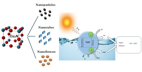
Surveying the Synthesis, Optical Properties and Photocatalytic Activity of Cu3N Nanomaterials

Institute of Forestry and Engineering Sciences, Estonian University of Life Sciences, Kreutzwaldi 56/1, 51014 Tartu, Estonia
*
Author to whom correspondence should be addressed.
Nanomaterials 2022, 12(13), 2218; https://doi.org/10.3390/nano12132218
Submission received: 23 May 2022 / Revised: 20 June 2022 / Accepted: 23 June 2022 / Published: 28 June 2022
(This article belongs to the Special Issue Functional Nanomaterials for Optoelectronics and Photocatalysis)

Abstract

:
This review addresses the most recent advances in the synthesis approaches, fundamental properties and photocatalytic activity of Cu3N nanostructures. Herein, the effect of synthesis conditions, such as solvent, temperature, time and precursor on the precipitation of Cu3N and the formation of secondary phases of Cu and Cu2O are surveyed, with emphasis on shape and size control. Furthermore, Cu3N nanostructures possess excellent optical properties, including a narrow bandgap in the range of 0.2 eV–2 eV for visible light absorption. In that regard, understanding the effect of the electronic structure on the bandgap and on the optical properties of Cu3N is therefore of interest. In fact, the density of states in the d-band of Cu has an influence on the band gap of Cu3N. Moreover, the potential of Cu3N nanomaterials for photocatalytic dye-degradation originates from the presence of active sites, i.e., Cu and N vacancies on the surface of the nanoparticles. Plasmonic nanoparticles tend to enhance the efficiency of photocatalytic dye degradation of Cu3N. Nevertheless, combining them with other potent photocatalysts, such as TiO2 and MoS2, augments the efficiency to 99%. Finally, the review concludes with perspectives and future research opportunities for Cu3N-based nanostructures.

Graphical Abstract

1. Introduction

The production of nanoscale structures has attracted interest as they exhibit size and shape-dependent physical, electrical and chemical properties that are absent in their bulk counterparts [1,2,3]. Transition metal nitride nanostructures such as Co2N [4], TiN [5], OsN2 [6], Zn3N2 [7] and IrN2 [8] are rising as strong candidates for a variety of industrial applications, as they display excellent catalytic, electrochemical and optoelectronic properties. Transition metal nitrides simultaneously behave as ionic crystals, transition metals and covalent compounds [9]. They are therefore being investigated as potential contenders for electrochemical energy conversion, heterogeneous catalysis, fuel cells, batteries and supercapacitors [10,11,12,13,14]. Additionally, their optical absorption, electrical properties and tolerance to structural defects make them a new class of semiconductors of interest [15]. The most popular metal nitrides in the semiconductor family are GaN, AlGaN and InGaN, which produce blue light-emitting diodes (LEDs) and lasers [16,17,18]. Furthermore, semiconductors, such as Ta3N5 [19], InN [20,21] and InGaN [22,23], are also potential candidates for photocatalysis due to their simple chemical composition, tunable narrow band gap and high stability. However, the metals, i.e., In, Ta and Ga, are relatively rare in the Earth’s crust, and the price of indium has shot up by 900% in the last 10 years. Therefore, more sustainable metallic raw materials are required for industrial applications.
In that regard, Cu3N, composed of earth-abundant elements, is a potential candidate for industrial applications. Moreover, owing to its cost-effectiveness of production and environmental friendliness, it has gained importance. In addition, due to its physicochemical characteristics and tunable optical and electrical properties, Cu3N is the focus of several research investigations [24,25]. The shape and size-controlled synthesis of Cu3N nanoparticles is one of the main challenges today. The current synthesis methods usually involve the use of reactive nitrogen precursors, high pressure and temperature [26]. Synthesis techniques, such as thermal decomposition [27], electroplating [28], solvothermal [26], chemical vapor deposition (CVD) [29], radio-frequency (RF) and direct current (DC) magnetron reactive sputtering [30,31,32] have been employed for the synthesis of Cu3N thin films. For nanoparticle synthesis, several reports claim that solution-based synthesis approaches tend to offer a better way of controlling the morphology and properties of Cu3N nanoparticles [24,33] by carefully varying the synthesis conditions, i.e., time, temperature and precursors. Although Cu3N itself has been extensively studied during the last decade, there is still a significant disparity between the theoretical and experimental optical band gaps. Nevertheless, all these studies concede that Cu3N has a narrow bandgap with values ranging from 0.2 to 2.0 eV, exhibiting either metallic or semiconductor behavior [30,34,35]. In fact, the physical and chemical properties of the material not only depend on the synthesis conditions but also on the presence of dopants in the Cu3N lattice [36,37].
Cu3N has been introduced as a new class of materials for the next generation of photovoltaic and photocatalytic applications due to its high optical absorption, good electrical properties and p-type defect-tolerant semiconductor characteristics [38,39,40]. Photocatalysis is an advanced oxidation process in which illumination is used to separate excitons that are then transferred to the surface of the nanoparticles [41]. The oxidation–reduction reactions produce reactive oxygen species (ROS) that oxidize organic matter on the surface of the nanomaterial leading to its degradation. The mechanism is explained in detail in Section 4 of this review. According to Cheng et al., transition metal nitrides are capable of reducing the overpotential or activation energy for photocatalytic reactions by providing additional active sites that promote electron–hole separation [39]. Furthermore, improvement in the catalytic yield of Cu3N has been achieved by doping with transition metal ions, such as Au, Ni, Cr, Fe and Co, at the interstitial sites of the cubic structure. In addition, some metallic nanoparticles such as Ag, Au and Cu display localized surface plasmon resonance (LSPR) that enhances their optical and electrical properties. In general, metal–semiconductor junctions tend to enhance the physicochemical performances of the heterostructures [38,42].
This review attempts to provide the first comprehensive compilation of the current research on synthesis approaches, electronic structure, optical properties and photocatalytic activity of Cu3N nanostructures. Herein, we analyze the effect of synthesis conditions on the precipitation of Cu3N and the formation of secondary phases of Cu and Cu2O, with emphasis on shape and size control. In fact, synthesis conditions determine the shape, size and surface defects of the nanoparticle. These have a direct on influence the electronic structure and subsequently on the band gap, optical and photocatalytic properties of the materials. Furthermore, it summarizes the emerging applications of Cu3N in photocatalysis, and for the first time, to the best of our knowledge, a possible photocatalytic reaction mechanism of Cu3N is proposed. The outlook of the material in commercial applications and future research is described in the summary and outlook section.

2. Synthesis of Cu3N Nanomaterials

During the last decade, significant progress has been made in the nitride chemistry synthesis field. The main synthesis routes consist of solid–gas state synthesis, solvothermal, sol-gel, non-thermal plasma, electrospinning, electrodeposition, atomic layer deposition, chemical vapor deposition and laser ablation methods among others [43,44,45]. These new strategies for nanomaterial synthesis must consider the reaction conditions, along with the most relevant precursors in order to obtain reliable and reproducible properties of the synthesized materials. Compared to metal oxides, carbides, sulphides and oxynitrides, the synthesis of metal nitrides is relatively challenging due to the requirements of inert conditions during the growth process in order to suppress the formation of copper oxide. In addition, metal nitride nanostructures also tend to oxidize in ambient conditions, making their stability a challenging issue.
In particular, synthesis routes for Cu3N nanomaterials can be divided into chemical and physical. The chemical methods have been the focus of recent research for the synthesis of Cu3N nanoparticles, as they offer better control of the morphology and particle size distribution during the synthesis process. However, maintaining a controlled inert atmosphere in order to impede the formation of secondary phases (Cu, CuO and Cu2O) remains a concern. Alternatively, physical methods mostly focus on thin-film growth. In both methods, the growth of Cu3N nanomaterials requires different types of N sources, including metal-nitride, ammonia, alkylamines and nitrogen-based reagents. Solid–gas-state synthesis consists of Cu precursors reacting with nitrogen gas. On the other hand, solution-based syntheses are usually carried out in non-aqueous media in order to avoid oxidation. The synthesis methods for Cu3N nanostructures are summarized and discussed in detail below (Table 1).

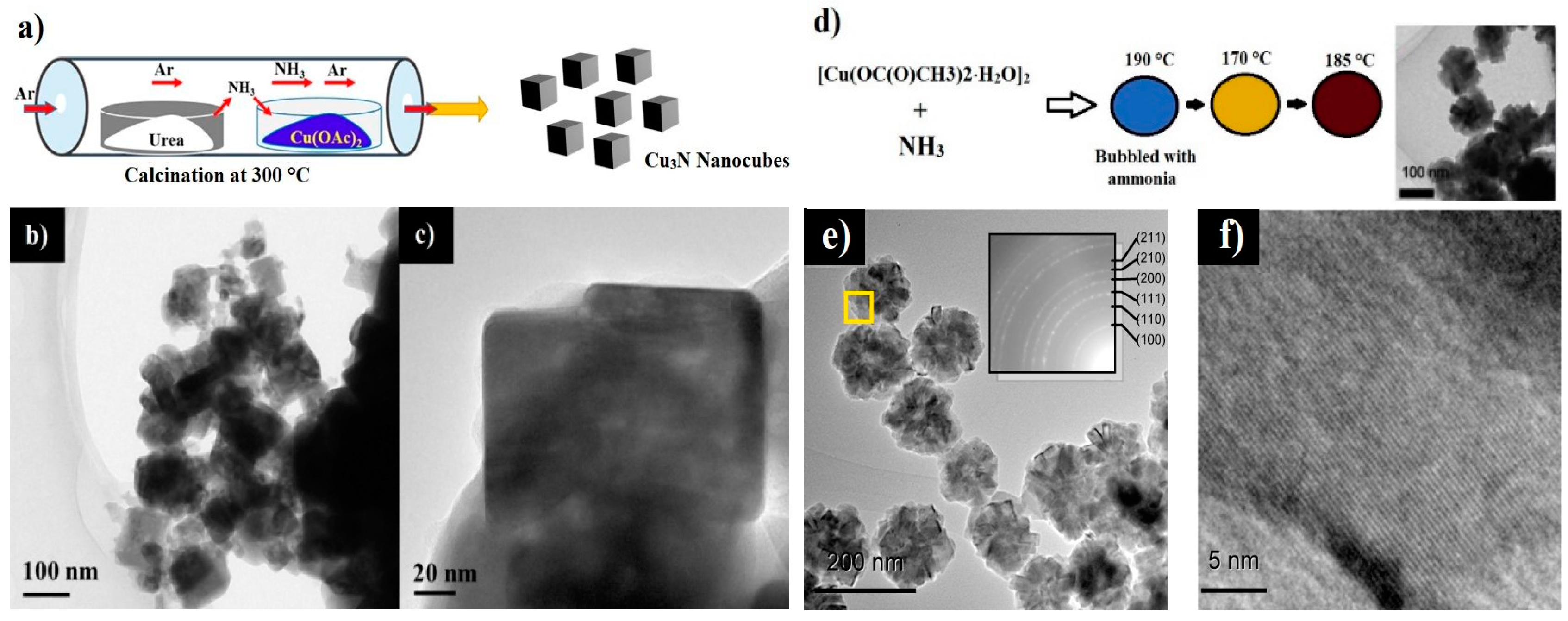
2.1. Gas-state Synthesis and the Ammonia Source

In this method, the corresponding Cu-based metal precursor undergoes nitration under gas flow (i.e., NH3 or a mixture of N2:H2) to produce Cu3N nanostructures [72]. A variety of N-rich complexes, including hydrazine, urea, ammonium salt, carbon nitride and their mixtures, act as nitrogen sources in order to tailor the nanoparticle size and shape. Nevertheless, ammonia gas for ammonolysis has been widely used as it creates a reductive atmosphere and simultaneously acts as a powerful nitrogen source [73]. In ammonolysis, the reaction time, temperatures under 200 °C, heating and cooling rates, as well as the amount of ammonia are often adjusted in order to optimize the reaction conditions and the nanoparticle features. In addition, the properties of the produced nitride depend on the precursor and preparation conditions, such as heating rate and final temperature. For example, Panda et al. reported a method for the synthesis of Cu3N nanocubes by nitration of copper acetate at 300 °C inside a quartz tube, based on the in situ decomposition of urea leading to the release of ammonia, as shown in Figure 1a. Their TEM results show that the Cu3N nanoparticles are cube-shaped with particle sizes ranging from 60–100 nm presented in Figure 1b,c [46]. On the other hand, Nakamura et al. used cooper (II) acetate monohydrate in an alcoholic solution of 1-nonanol along with bubbling ammonia for 1 h at 190 °C to produce Cu3N nanoflowers (Figure 1d–f) [53]. In their study, the nanoparticles had granular shapes with a diameter of less than 200 nm. The differences in morphology and size arise from a combination of copper precursors, synthesis temperature and nitrogen sources. The utilization of urea as a nitrogen source, as opposed to NH3, is very advantageous owing to facile handling and controllability of flux, implying that the risk of over-reduction of copper acetate to form metallic copper is mitigated [46]. The mechanism of nanoparticle formation was elucidated by Nakamura et al. and followed certain reaction steps: (1) formation of copper (II) amine complex, (2) reduction, by the long-chain alcohol, of Cu2+ to Cu+ and (3) the reaction between ammonia and Cu+ [53].
Multistep synthesis approaches have also been applied to the synthesis of Cu3N. These approaches are used to reduce copper oxide nanoparticles produced in the first step of the synthesis, followed by nitration. For example, Szczesny et al. synthesized Cu3N nanoparticles with diverse morphologies from oxygen-containing precursors using a two-step process that combines solvothermal and solid–gas ammonolysis stages [74]. In the first step, copper (II) chloride dihydrate was used as a precursor for the fabrication of copper (II) oxide and copper (II) hydroxide nanoarchitectures by solvothermal methods. In the second step, Cu3N was obtained through ammonolysis of Cu(OH)2 and CuO nanoparticles [74]. Deshmukh et al. synthesized Cu3N@SiO2 composites using a multistep approach [71]. First, CuO nanoparticles were synthesized within hollow mesoporous silica spheres by binding or adsorbing Cu2+ ions onto the surface of carbon spheres, followed by the formation of a mesoporous silica shell by a sol-gel method. Cu3N nanoparticles (size < 30 nm) were formed within silica spheres through the nitration of copper (II) oxide composite (CuO@SiO2) with ammonia gas at 300 °C for 10 h [71]. In the two-step approach, chemical nitration can only occur after the copper oxide is reduced to copper ions, which then react with ammonia to form Cu3N. During the synthesis, a change in the color of the solution from yellow to brown indicates the reaction of copper ions with ammonia leading to the precipitation of nitride nanoparticles [62]. Furthermore, Nakamura et al. suggested that for successful nitration, ammonia must come into contact with the copper ions at an optimum temperature as soon as the reduction of copper oxide starts [53].
The ammonolysis reactions provide a versatile route to synthesize Cu3N nanoparticles. Based on reports, ammonolysis is performed under specific conditions in solid-state chemistry in order to obtain a complete exclusion of oxygen and water during synthesis and handling. In addition, this approach can be optimized by varying the solid precursor, ammonia flow rate, heating and cooling rates, temperature and reaction time. However, the control of the nanoparticle shape and size in these processes remains a challenge. Moreover, this pathway involves the use of NH3, which is toxic and corrosive at high temperatures.

2.2. Solution-Based Synthesis

In addition to ammonia gas, nitrogen-based compounds can also be used as nitrogen sources for the synthesis of Cu3N nanostructures. In consequence, the use of non-aqueous solutions in the synthesis of metal nitrides has gained interest, as it suppresses oxidation and allows controlling the nanoparticle size and shape. The technique of non-aqueous synthesis requires water or hydrate-free solvents, as well as regulated temperatures and pressures in a controlled environment, as it relies primarily on the solubility and reactivity of precursors at relatively high temperatures and pressures [75]. Primary amines are commonly used as capping agents to synthesize metal nitrides and semiconductor nanomaterials. In general, solvothermal methods offer good control of the shape, size and crystallinity of nanostructured materials by controlling synthesis parameters, such as reaction time, temperature, precursor, surfactant and solvent, in order to vary the physical and chemical properties of the nanomaterials [76].

2.2.1. Effect of Solvent

Presently, the thermal decomposition of copper salt-based precursors in long-chain amines or alcohols is one of the most popular synthesis techniques for Cu3N nanoparticles. It not only serves as a nitrogen source but can also performs simultaneous functions as a solvent, surface stabilizer and reducing reagent. Therefore, special attention is being paid to the synthesis of Cu3N nanoparticles using solvents, such as 1-octadecene (ODE) and amine sources, including 1-octadecylamine (ODA), hexadecylamine (HAD), oleylamine (OAm) and benzylamine (BZA) [33,38,47,49,54,63,77]. Synthesis of Cu3N nanocubes with tunable sizes was reported by Wu et al. through the decomposition of Cu(NO3)2 in ODE with different capping agents by a facile one-step process [47]. The nanoparticle size depended on the amine source used and ranged from 10 to 30 nm. In fact, the size was reduced significantly to 26 nm with ODA, to 18.6 nm with HAD and even further to 10.8 nm with OAm [47]. A similar synthesis approach for Cu3N nanocubes using ODA and ODE was also reported by Wang et al. [49]. They obtained Cu3N nanocubes (size = 15 nm) in Figure 2a after the thermal decomposition of Cu(NO3)2⋅3H2O at 240 °C in ODA solvent [49]. Similarly, Barman et al. reported the synthesis of Cu3N nanocubes with an average particle size of ~10 nm using a 1:1 volume ratio of ODE and OAm solvents [38]. The TEM image consists of smaller nanoparticles that coalesce into a nanocube, as visible in Figure 2b.
In addition, different solvents and reaction parameters influence the size and morphology of the nanoparticles. For example, Princ et al. synthesized two types of Cu3N nanoparticles with different morphologies using two different capping agents dissolved in ODE [63]. The report revealed that when OAm is used as a capping agent, spherical nanoparticles of 8 nm were produced (Figure 2d). In contrast, HAD produces cube-like nanoparticles of 50 nm (Figure 2e) [63]. Sithole et al., in two different reports, synthesized Cu3N nanoparticles and Cu3N nanocubes using amines as solvents [24,48]. Cu3N nanoparticles with an average particle size of 2.8 nm were synthesized using pyrrole-2-carbaldpropyliminato Cu(II) (PPC) as a single-source precursor with ODA [24]. On the other hand, Cu3N nanocubes with an average size of 41 nm, Figure 2c, were synthesized using Cu(NO3)2⋅3H2O at 240 °C in ODA [48]. Finally, Deshmukh et al. reported the synthesis of ultrasmall Cu3N nanoparticles of ~2 nm, Figure 2f, via a one-step reaction of copper (II) methoxide (Cu(OMe)2) precursor with BZA at lower temperatures for short reaction periods (e.g., 140 °C for 15 min) [54].

2.2.2. Effect of Capping Agent

The above results suggest that the nanoparticle size and shape vary as a function of capping agents or surfactants. In fact, the long-chained amine surfactant plays an important role in shaping the nanoparticles at the nucleation and growth stages. They modify the decomposition routes of the copper nitride (II) reagent contrarily to other solvents or solid-state processes. According to Princ et al., the reasons for differences in the overall morphologies of nanoparticles using different capping agents may be related to the different mesocrystal subunits or the subsequent crystallographic orientations of subunits [63]. From the TEM images of Figure 2b–d, the coalescence of small spherical nanoparticles into nanocubes could also be another mechanism. The formation of nanocubes via such a mechanism appears to be more favorable in the case of long-chained amines. In fact, the subunits of nanocrystals are subject to various competitive forces, such as van der Waals, dipole–dipole and dissolution. Nonetheless, it is important to mention that so far, there is no report that elucidates the effect of the amine chain length on the size and morphology of the nanoparticles. Nevertheless, a complex combination of the synthesis environment, reaction time, temperature and amount of reagents influence the final shape and size of the nanoparticles.

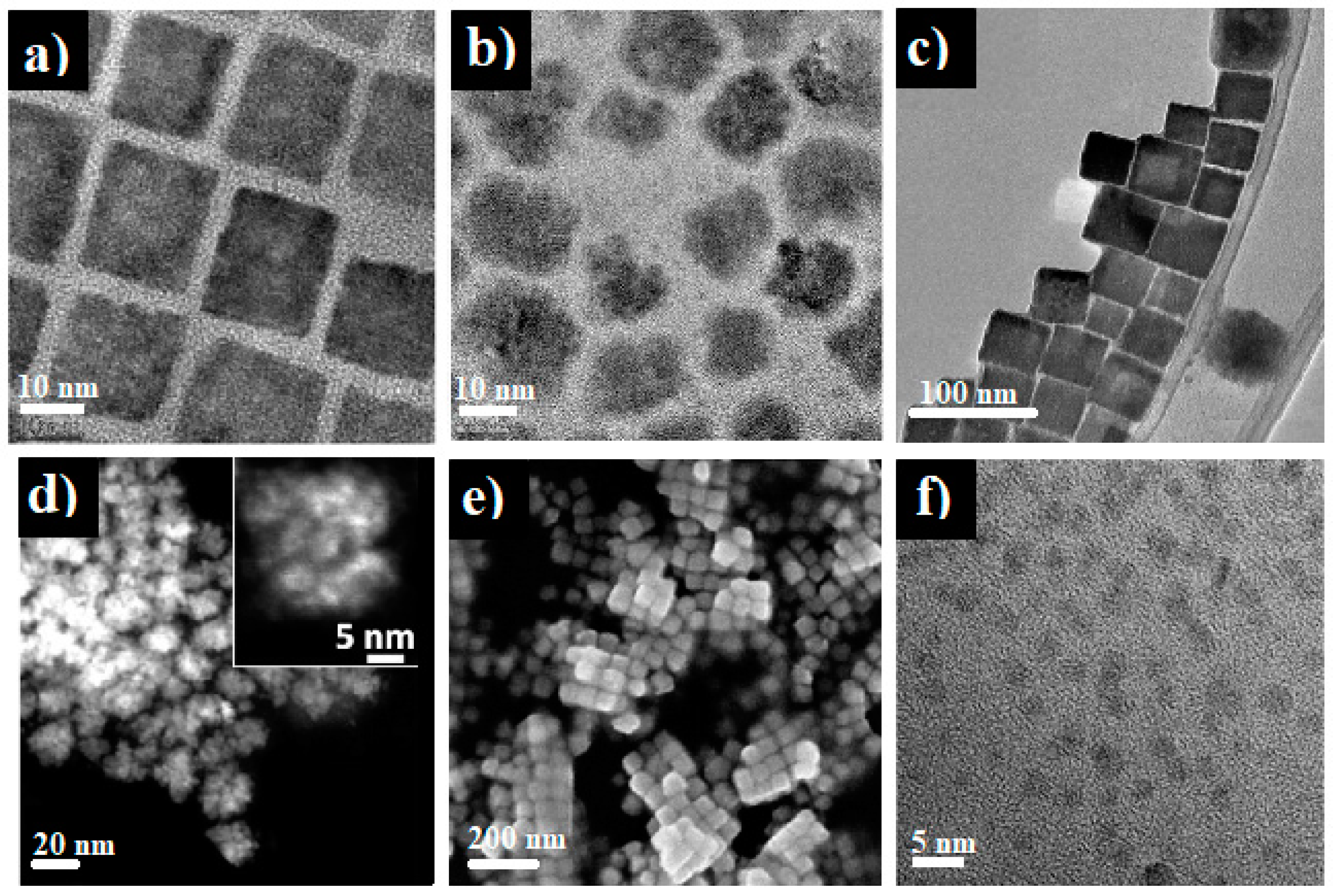
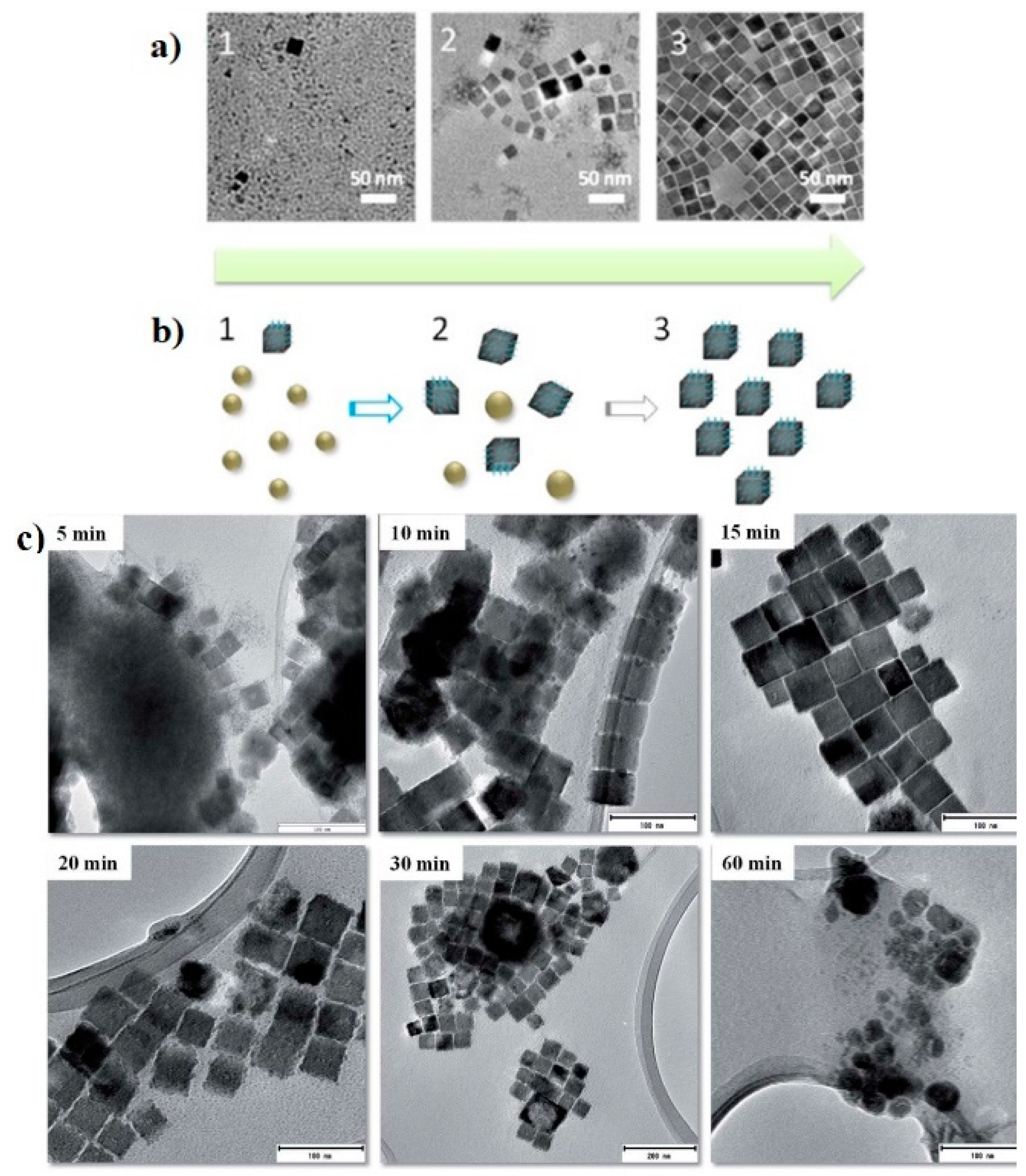
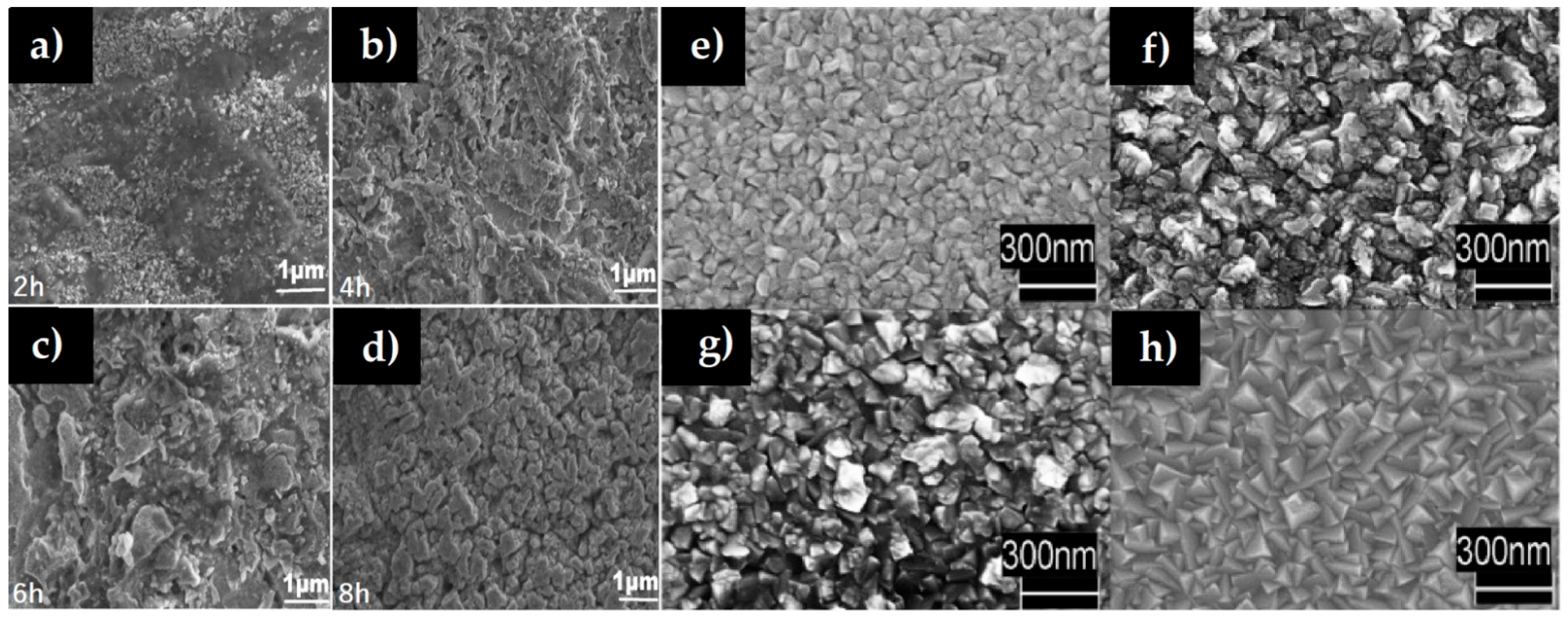
2.2.3. Effect of Reaction Time

The reaction time related to the formation mechanism of Cu3N nanoparticles (nucleation, growth, aggregation and breakage) is a primary factor to be considered. It has been reported that the nanoparticle size, shape and stability are strongly dependent on the reaction time [78]. For example, Xi et al. reported the solvothermal synthesis of magnetic Cu3N nanocubes with high electrocatalytic reduction properties [50]. The cube-shaped Cu3N nanoparticles were synthesized by dissolving copper (II) nitrate in organic solvents of ODA and OAm at a high temperature of 240 °C. The detailed growth process of Cu3N nanocrystals is shown in Figure 3a,b, consisting of three different stages: (1) nucleation stage to form nanoparticles, (2) growth stage in which the nanoparticles adopt the cubic shape, owing to the surface tension exerted by the solvent and (3) molding stage in which nanocubes are formed [50]. In addition, Sithole et al. (shown in Figure 3c) reported a fourth step, i.e., the transformation of Cu3N into Cu nanoparticles [33], which is due to a spontaneous decomposition of Cu3N nanocubes depending on the reaction time. In fact, a cloud of nuclei with a few developed Cu3N nanocubes was obtained after 5 min, followed by well-defined nanocubes after 15 min. Finally, after 20 min of heating, degradation of the nanocubes occurs, and the copper nitride decomposes into metallic Cu within 60 min.

2.2.4. Formation of Secondary Phases

Both routes have their share of advantages and drawbacks. One common disadvantage is the precipitation of secondary phases during Cu3N synthesis. For instance, it is reported that by prolonging the reaction time at a particular temperature, a partial phase transformation of Cu3N into Cu and Cu2O occurs [63]. Kieda et al. applied a spray pyrolysis technique using a copper–amine complex solution. However, obtaining a pure phase of Cu3N using only Cu2CO3(OH)2 precursor [79] is unlikely, as the co-precipitation of Cu, Cu2O and CuO secondary phases is inevitable. On the other hand, changing the molar ratio of the reactants (Cu(NO3)2⋅3H2O:ODA) results in the formation of Cu and Cu2O nanocrystals with or without Cu3N [33]. The formation of CuO is suppressed most likely due to a more reductive synthesis environment. Therefore, the development of a scalable, reliable and reproducible method for the synthesis of high-quality Cu3N nanostructures with a high density of active sites is the need of the hour. Additionally, the degassing process, which removes water molecules from the solution, is an important step in suppressing the formation of secondary phases. The most commonly used gases are nitrogen or argon, which eliminate water molecules from the solution while heating the solution between 100 °C to 150 °C. Wet chemical routes tend to be more reliable and reproducible in controlling nanoparticle shape and size compared to gas-state methods, thus making them viable for larger-scale production. Major limitations in upscaling these methods include high reaction temperatures and the use of surfactants, which increase their costs and complexity.

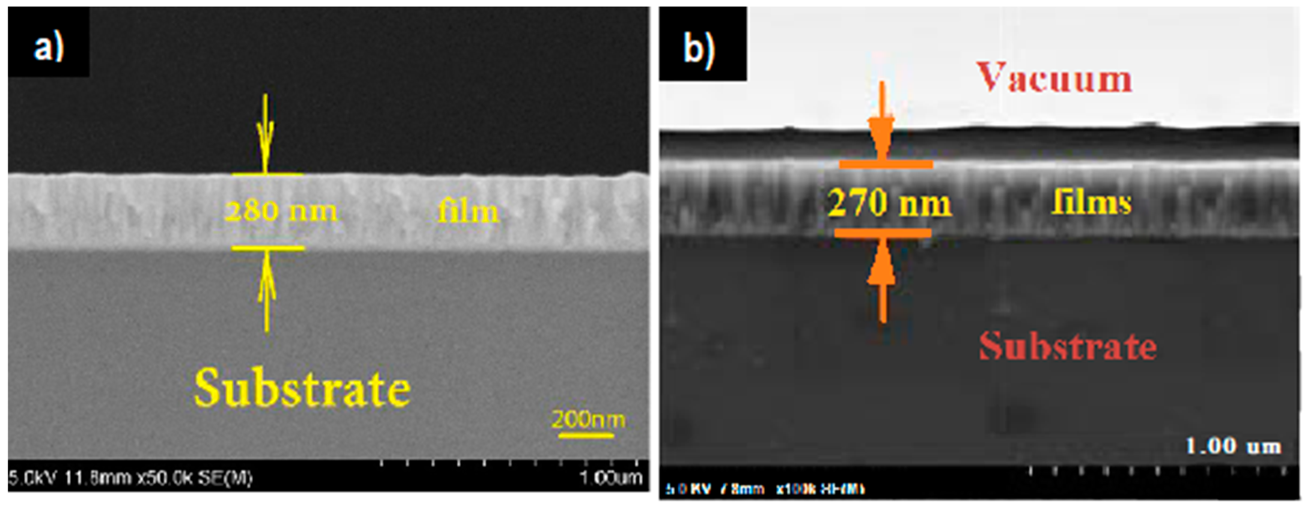
2.3. Thin Film Deposition Techniques

Several studies have focused on the growth of Cu3N thin films. A number of techniques, such as DC and RF reactive magnetron sputtering, thermal evaporation, pulse laser deposition (PLD) and CVD, are commonly used to grow Cu3N thin films. These deposition techniques produce nitride thin films with controlled stoichiometry, thickness and composition [39]. In fact, the efficient thin film deposition of Cu3N has mainly been achieved via physical methods for applications in optical data storage [80], solar energy conversion [15], BioMEMs [81] and photovoltaics [82]. In general, physical methods are useful for growing single-phase thin films but have the drawback of producing only a limited variety of compounds [76]. Furthermore, the doping of Cu3N with other compounds has marked a breakthrough in nitride thin film research. In that regard, thin-film deposition techniques provide a simple pathway to introduce foreign atoms while retaining the Cu3N lattice stability.
Most of the previous work on Cu3N nanostructures has been on thin film deposition using magnetron sputtering. The method is often used to produce transition metal nitride thin film electrodes, which exhibit excellent adhesion, controllable composition and thickness of nanostructured films with excellent electrochemical properties [83]. During the reactive sputtering of Cu3N, a reductive gas such as N2 or Ar reacts with a Cu metal or a Cu3N target, sputtering off the compound layer. Then, the sputtered Cu and N species are deposited on substrates forming Cu3N compound layers [68]. For instance, Jiang et al. deposited Cu3N:Pb thin films using different Pb concentrations on monocrystalline silicon through DC and RF reactive magnetron sputtering [30]. In fact, Pb doping leads to a high adhesion of the films to the substrate, as it promotes nucleation in the early stages of thin-film growth [30]. Figure 4a shows the cross-sectional view of dense and well-adhered films. Similarly, Xiao et al. investigated the growth of Cu3N:Ag thin films using RF and DC magnetron sputtering (Figure 4b) [69]. In this research, Cu3N:Ag thin films were prepared with variable sputtering power of Ag. They observed that an increase in the Ag content brings about an increase in the grain size. Additionally, the optical band gap of the films also increases owing to the plasmonic-induced Burstein–Moss effect leading to an increase in the number of carriers in the conduction band of Cu3N, which in turn displaces the Fermi level towards the conduction band [69]. In both Ag and Pb doped thin films, the growth mode is columnar, typical of the sputtering deposition process. However, the roughness of the Pb doped films is higher than the Ag-doped films, most probably due to the Pb atom being slightly larger than the Ag atom. Since the lattice mismatch for Pb doped films is higher, the lattice relaxation process enhances the thin film roughness. Similarly, nanocomposites of Cu3N tend to have enhanced optical properties. For example, TiO2-Cu3N nanocomposites manifest an improved bandgap compared to Cu3N alone. Zhu et al. also reported the growth of TiO2-Cu3N and Cu3N-MoS2 nanocomposite films by magnetron sputtering that demonstrate enhanced photocatalytic properties [35,84]. Both TiO2 and MoS2 are n-type semiconductors that, when combined with p-type Cu3N, create p-n junctions. For catalytic activity, large specific surfaces of active materials are required. Moreover, when the roughness increases, the number of active sites on the surface also augments, which leads to an enhancement of photocatalytic activity [35,84]. Industrially viable thin film growth techniques, such as sputtering, allow thickness control with the possibility of depositing on large surface areas in order to obtain a high specific surface. The deposition parameters of Cu3N thin films include sputtering power, N2 pressure r (r = N2/[N2+ Ar]), substrate temperature and deposition pressure, which have a significant influence on Cu3N thin film growth and their properties. Additionally, deposition parameters also affect the crystal orientation and grain size of Cu3N thin films [65,83].
Cu3N thin films can also be deposited by thermal evaporation using nitrogen as a gas source. In this method, the Cu powder is evaporated onto a glass substrate and then exposed to N2 gas in order to fabricate Cu3N thin films. Ali et al. thermally evaporated Cu powder on a glass substrate in a horizontal glass tube furnace at 1000 °C in a high vacuum for 25 min [67]. Then, the temperature of the tube furnace was set to 300 °C, and an N2 gas flow rate of 100 sccm was maintained for different reaction times. Figure 5a–d show the SEM images of Cu3N thin films deposited for a duration of 2, 4, 6 and 8 h under nitrogen gas flow at 300 °C. When the growth time is prolonged, an increase in the grain size is observed [67]. Cu3N thin films with a rough surface were deposited by Lindahl et al. using a gas pulsed CVD [29], which is a gas phase chemical method by which thin films are grown on a suitable substrate through precursor decomposition at elevated temperatures. In that case, Cu-Ni-N thin films were prepared using CVD processes with intermittent NH3 gas flow. Ni-doped Cu3N can be described as a solid solution of Ni in Cu3N formed in a pseudo-binary system composed of the two metastable phases Cu3N and Ni3N (Figure 5b). According to Lindahl et al., the texture of the deposited films changes with the increase of Ni content, which was attributed to changes in the deposition mechanism through the probable occupancy of the interstitial sites of Cu3N in the crystal structure [29].

3. Electronic Structure and Band Gap

Cu3N has a primitive open anti-rhenium trioxide cubic structure (space group Pm3m, lattice constant a = 3.82 Å), presented in Figure 6 [85]. In the structure, N atoms occupy the cube corners of the unitary cell in (0, 0, 0) and Cu atoms are located between two consecutive nitrogen atoms in (½,0,0), (0, ½, 0) and (0, 0, ½) [26,51,86,87]. Each N atom in the cubic structure of Cu3N is shared by eight cells, while each Cu atom is shared by four cells. In pure Cu3N, the face centers and the body of the cube are empty. These void interstitial sites are, therefore, available to host Cu, N or other foreign atoms under certain conditions [88]. However, the insertion of additional metallic elements in the body of the Cu3N lattice alters the chemical interactions between Cu and N, thereby modifying or changing the electrical and optical properties. Experimental and computational studies reveal that metal-doped Cu3N adopts metallic characteristics due to the reduction of the metallic inclusions (M0) [88]. For instance, Hahn et al. demonstrated that Cu3N is a semiconductor, while Cu3N-Pd exhibits semi-metallic conductivity due to Pd atoms causing modifications in the energy bands [89]. Additionally, Cu3N:Pd presents higher mass activities and stability in comparison with commercial Pd alone. In addition, Moreno et al. established that the addition of an extra Cu atom into the body of the unitary cell of Cu3N endows it with metallic properties [90]. In turn, the unit cell of Cu3N expands, owing to the progressive insertion of Cu atoms. Furthermore, their computational studies show that the lattice parameter of Cu3N-Cu expands by 0.06 Å. Moreno et al. inferred that Cu3N with lattice constants higher than 3.868 Å behave as conductors [90]. Finally, these types of doped-compounds, i.e., Cu3MxN, present an anti-perovskite structure, owing to the metal dopant occupation of (½, ½, ½), i.e., the body-center position [88]. Anti-perovskite structures consist of interchanged A and B site atoms. They are defect tolerant, present excellent ionic conductivities and are ideal candidates for electrodes of batteries [91]. This suggests that they possess interesting redox capabilities, enabling their application as photocatalysts.
Furthermore, the crystal chemistry of transition metal nitrides is largely dictated by the bond coordination of N and M atoms. In these compounds, the M atoms are bonded with nitrogen via covalent or ionic bonds. According to Rao et al., the addition of N atoms to a transition metal converts the metal–metal bond to a covalent bond or a mixture of covalent–metal bonds [44]. Moreover, the addition of N increases the bond length and, consequently, the lattice parameters, resulting in a contraction of the metal d-band, further suggesting that bonds in metal nitrides are ionic. This d-band contraction causes an increased density of states (DOS) near the fermi level, giving rise to novel catalytic properties, which are different from the parent metal but rather similar to noble metals [14]. Moreover, recent studies suggest that both covalent and ionic bonds connect Cu and N atoms in undoped Cu3N [30]. On the other hand, for M-doped Cu3N, the bond coordination has a covalent character as the interactions between the inserted M and Cu atoms dominate [42,92].
Undoped Cu3N tends to be insulating due to defect states created by metallic and non-metallic vacancies of Cu and N, respectively [93]. However, due to the varying nature of the vacancies giving rise to shallow defect states, the bandgap of Cu3N shows variations and ranges from 0.2 to 2.0 eV. Another study demonstrated that doping with iodine gives rise to states that are located very close to the band edges and therefore resulting in the absence of band gap states [94]. Furthermore, Cu3N being a p-type semiconductor, displays a strong hybridization of the Cu 3d and N 2p orbitals close to the valence band owing to their anti-bonding states, which causes their high tolerance to defects. Theoretical calculations confirm that Cu 3d electrons are a major contributor to the DOS and have an important influence on the Cu3N band gap.
Since nanostructured defect-tolerant transition metal nitrides possess semiconducting properties with band gaps corresponding to visible wavelengths, they are therefore considered suitable materials for photocatalysis and photovoltaic applications [39,95]. In the literature, there are several discrepancies in the band gaps of Cu3N arising from both theoretical and experimental studies. Theoretical calculations predict an indirect band gap ranging from 0.23 to 1.0 eV depending on the calculation method [58,88]. Density Functional Theory (DFT) tends to underestimate the band gap mainly due to self-interaction errors and changes in potential upon changing the number of electrons in the conventional framework of DFT [96]. Co-workers also calculated the band structure and DOS before and after the addition of a foreign atom into the cubic structure of Cu3N. In fact, the electronic structure changes in the presence of foreign atoms, accompanied by an increase in the Fermi energy, along with a consequential change in the band gap. For instance, computational calculations reveal that pure Cu3N is a semiconductor with a small indirect band gap equal to 0.38 eV. In contrast, for M-doped Cu3N (M = Sc, Ti, V, Cr, Mn, Fe, Co and Ni), the band gap becomes negligible, giving rise to the metallic character of Cu3N [42]. Other studies confirm a semiconducting behavior but suggest that pure Cu3N presents an indirect band gap of 0.32 eV and direct gaps of 1.09 and 0.87 eV, whereas for Cu3N-N rich compounds, a partially filled spin-resolved narrow band of new electronic bandgap states at the Fermi energy is observed [97]. This new band modifies the optical properties of Cu3N and makes the material susceptible to infrared absorption.
On the other hand, experimental results ascertain both direct and indirect band gaps ranging from 1.17 to 2.38 eV that depend on the experimental conditions and N content. Table 1 summarize the synthesis parameters and band gaps of Cu3N and Cu3N-M nanostructures. Band gaps determined experimentally vary, for example, between 1.91 to 2.15 eV for Cu3N thin films deposited by sputtering, whereas a maximum band gap of 2.92 eV was reported for nanoparticles of Cu3N [52]. Furthermore, band gaps of 1.04 eV (indirect) and 1.5 eV (direct) were obtained from cyclic voltammetry (CV) measurements on Cu3N nanocubes based on onset Redox potentials [47]. In general, the experimental band gap depends on the synthesis conditions, which in turn determines the morphology and chemical composition of the nanomaterial.

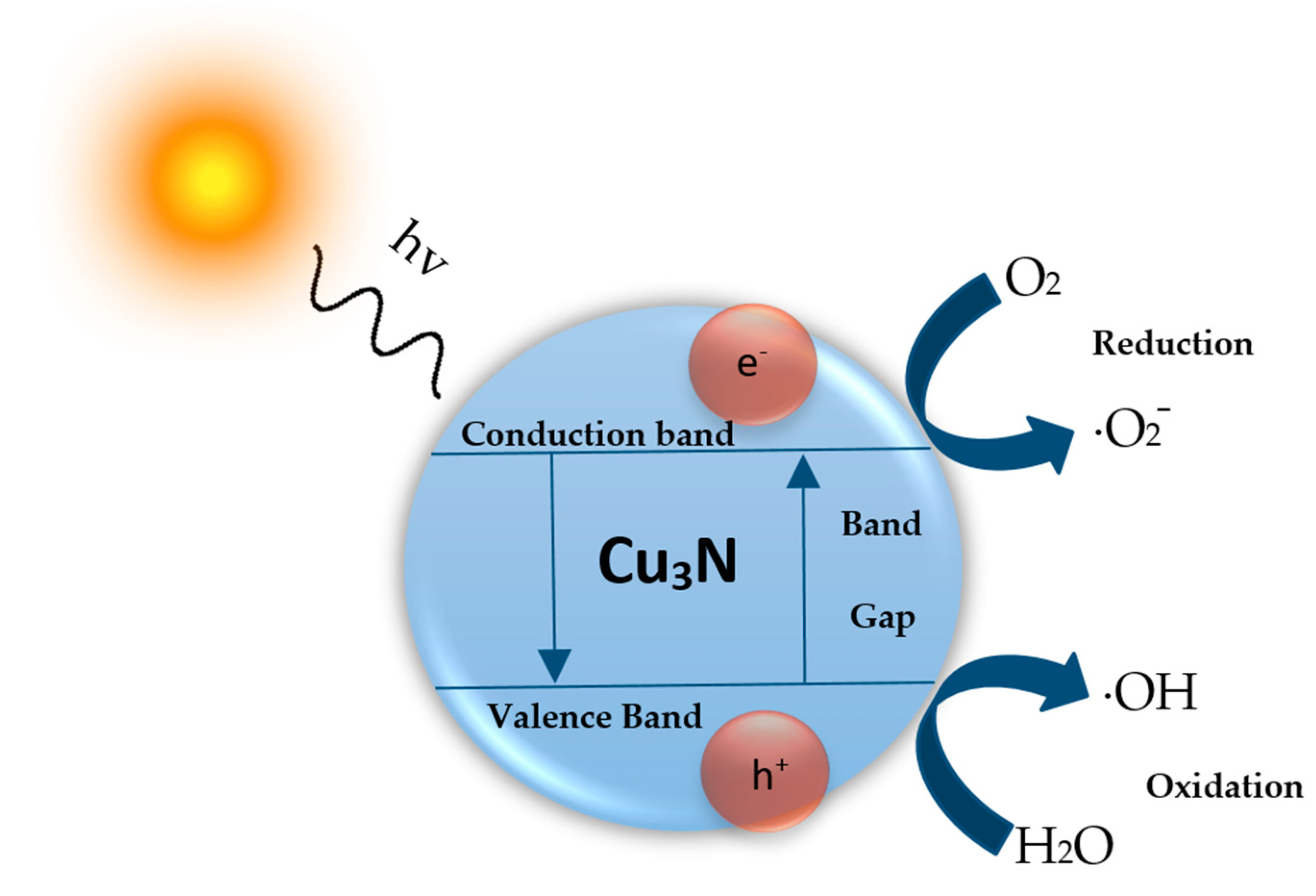
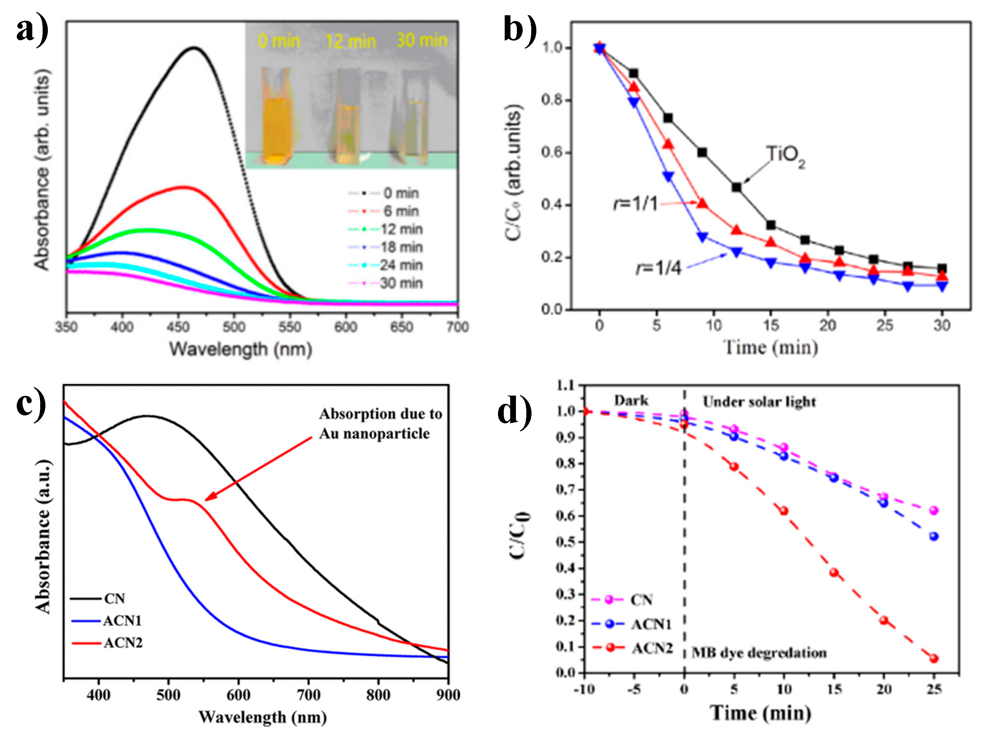
4. Photocatalytic Activity of Cu3N Nanoparticles

Photocatalysis is a redox process involving three main steps: (i) the generation of electron-hole pairs (e/h+) by photoexcitation, (ii) transportation of the excitons to the semiconductor surface and (iii) the utilization of charge for surface oxidation–reduction reactions [39,41]. The total efficiency in these processes is strongly determined by the properties of the semiconductor photocatalyst, such as the electronic structure, band gap, surface properties along with kinetic and thermodynamic processes [98]. An ideal photocatalytic material should primarily have a bandgap that is optimal for absorbing in the entire range of the solar spectrum in order to dissociate water molecules while retaining its stability during the reaction process. In addition, it must be cost-effective, easy to process, readily available and non-toxic. Moreover, in order to efficiently harvest visible light and accelerate reactions, the band gap should preferably be under 3.2 eV. However, since redox reactions require a certain amount of energy, narrow band gap semiconductors may therefore not be the most suitable for catalytic reactions. In addition, the probability of excitonic recombination increases for lower bandgaps. Therefore, an optimum balance between the band gap and recombination lifetime is required. One method for efficient charge separation is the combination of plasmonic nanoparticles with photocatalytic semiconductors.
Current reports demonstrate a keen interest in the photocatalytic activity of metal nitride nanomaterials. Their metal-like properties, such as conductivity, optical band gap and visible light activation, are beneficial for highly efficient separation and delivery of photogenerated carriers. Unlike traditional semiconductors (oxides, sulfides and carbides), metal nitrides can lower the overpotential or activation energy for photocatalytic reactions on the surface of semiconductors. They also provide additional active sites and promote electron-hole separation at the interface of the co-catalyst [39,99]. Furthermore, their low-cost production, high thermal stability and tolerance against acids and bases are advantages in photocatalysis [39]. Inspired by these properties, the design and construction of semiconductor-based metal-nitride nanomaterials have been carried out and applied to photocatalytic processes for water splitting, organic dye degradation, CO2 reduction and decomposition. For example, CoN, [100] Ta2N, [100] Ta3N5, [101], Ni3N, [102,103] and InGaN [104] have been tested as potential semiconductors for water splitting. In photocatalytic water splitting reactions, the photo-induced process enables the production of H2 and O2 [44,105]. Additionally, metal nitrides are sturdy with good refractory properties at elevated temperatures of 2000 °C owing to their metallic character. The latter also dotes them with properties similar to plasmonic metal nanoparticles. However, compared to noble metal nanoparticles, nitrides display plasmonic wavelengths in the visible and infrared regions. For ex., TiN has been used as plasmonic interconnectors, further suggesting that nitrides can replace noble metals in such applications. Nitrides also display tunable optical responses and improved light-harvesting, equivalent to noble metals. They can, in general, significantly enhance the local electromagnetic field when the incident light interacts with the surface plasmons [44,106]. In other words, localized surface plasmon resonance (LSPR) enhances the electric field, facilitating light absorption and charge transfer processes of semiconductors [38,107]. In such cases, the generated excitons have higher energy than the Fermi level of the photocatalyst, which is ideal for driving photocatalytic reactions [108]. For example, ZrN [109], HfN [110] and TiN [111] are reported as plasmonic metal nitride nanostructures. However, Cu3N has not yet been specifically reported as a plasmonic nanomaterial. Nevertheless, synthesis routes tend to produce secondary phases of Cu metal, which is a known plasmonic material that enhances the overall catalytic performance of the primary phase [33]. In all cases, metal nitrides need to be combined with a metal or themselves possess a metallic character in order to display surface plasmon resonance. This is likely if they are synthesized with an excess of Cu in the case of Cu3N. In soft chemical synthesis, excess Cu could favor the co-precipitation of Cu metal and simultaneously incorporate Cu in the Cu3N lattice. For thin-film synthesis, the Cu metal phase separation can be suppressed by controlling the growth conditions in order to ensure the incorporation of Cu in the Cu3N lattice.
With further regard to Cu3N-based nanostructures, several studies have reported photocatalytic degradation of dyes. A schematic representation of the Cu3N-based photocatalytic process is represented in Figure 7. The process starts when Cu3N absorbs energy equivalent to its bandgap, whereupon generating a wide range of electron-hole pairs (e--h+) under the photoelectric effect. The e--h+ pairs migrate to different positions on the surface of the Cu3N under the action of the generated electric field. The electrons on the surface of Cu3N are then transferred to the adsorbed molecular oxygen, generating reactive oxygen species such as superoxides (•O2−). The holes react with water and hydroxyl ions to generate hydroxyl radicals (•OH) that can oxidize organic matter adsorbed on the surface of Cu3N. The oxidizing ability of •OH radicals is the most potent among reactive oxygen species in aqueous media. It is capable of oxidizing most of the inorganic contaminants, as well as organic matter in water and degrading them to smaller inorganic molecules such as carbon dioxide, water and other harmless substances. The possible chemical reactions of the photocatalytic activity of Cu3N are as follows:
Cu3N + hv → e + h+
h+ + H2O → •OH + H+
e + O2 → O2
OH + H+ dye →…→ CO2 + H2O.
In general, Cu3N demonstrates excellent electrochemical performance. Both photo- and electrocatalysis have the same mechanism of charge creation. The difference lies in the type of activation energy provided to create these charges. Therefore, electrochemistry can elucidate the redox reactions of Cu3N in order to evaluate its potential for hydrogen and oxygen production. Sajeev et al. evaluated the potential of Cu3N in hydrogen evolution reaction (HER), where they claim a lower overpotential than its oxide counterpart Cu2O [112]. In general, the shift from oxides to nitrides for photo- or electrocatalysis has been facilitated owing to the higher potential of N 2p than O 2p orbitals. This signifies that metal nitrides have a lower bandgap than metal oxides, whereby they are more adapted to photocatalysis. They can therefore be also employed as working photoelectrodes for photocatalytic water splitting. Nevertheless, Cu3N tends to be unstable in aqueous media and high and low pH conditions due to its tendency to oxidize. However, these concerns are surmounted by synthesizing nanocomposites of Cu3N [98], which are particularly useful for dye degradation in aqueous media. Cu3N is also used as an electrocatalyst in gas-phase reactions for the production of hydrocarbons via CO2 reduction reactions [113]. Presently, there are no accounts of photoelectrocatalytic production of hydrocarbons with Cu3N or its nanocomposites, even though the potential exists.
In recent years, several studies of Cu3N nanomaterials for photocatalytic applications have been reported (Table 2). Jiang et al. reported the photocatalytic degradation of methyl orange (MO) using Cu3N thin films with an optical band gap of 2.0 eV [65]. In this work, a MO solution of 20 mg/L in 50 mL water was used as the target degradation product and Cu3N thin films with dimensions of 2.5 cm × 1.0 cm × 120 nm as a photocatalyst under a high-pressure mercury lamp (500 W). A degradation yield of 95.5% in 30 min was achieved (Figure 8a). They infer that the effective photogenerated electron-hole pairs mainly originate from Cu vacancies and interstitials in the film [65]. Although the Cu3N thin-film alone presents excellent photocatalytic properties for degrading dyes, it has a few shortcomings. Therefore, Cu3N nanostructures are combined with other semiconductors. For instance, Zhu et al. demonstrated that the degradation of MO using TiO2@Cu3N thin films (effective band gap = 3.0 eV) is higher than in pure TiO2 thin films, as seen in Figure 8b [35]. A degradation rate of 99.2% of MO solution with an initial concentration of 20 g/mL using a 500 W mercury lamp for 30 min was obtained [84]. Other studies using Cu3N@MoS2 thin films (band gap = 2.05 eV) as photocatalysts obtained a 98.3% degradation rate of MO with an initial concentration of 10 mg/mL in 30 min. In this case, controlled quantities of MoS2 reduce the overall band gap of the nanocomposite to values lower than the band gap of Cu3N [35]. On the other hand, during the past few decades, researchers have also studied the photocatalytic activity of Cu3N nanoparticles in aqueous media. Sithole et al. reported the photocatalytic degradation of methylene blue (MB) and MO using Cu3N nanocubes with a band gap of 2.41 eV [48]. In that study, 0.1 g of Cu3N nanocubes were added into the solution of MB and MO, with an initial concentration of 20 ppm under a solar simulator (AM 1.5 G 100 mW/cm2). Degradation efficiencies of 89% of MO after 180 min and 61% of MB after 240 min were obtained. They argue that the difference in degradation efficiencies was due to differences in the chemical structure of the dyes. They affirm that catalytic reactions are more efficient in anionic than cationic dyes. Similarly, Barman et al. evaluated the photocatalytic degradation of MB and MO using Cu3N-Au heterojunction as a photocatalyst (Figure 8c) [38]. The Au-Cu3N heterostructures ACN1 (Au nanoparticle size is ∼5 nm) and ACN2 (Au nanoparticle size is ∼10 nm) exhibit enhanced photocatalytic activity in comparison with pure Cu3N nanocubes, mostly due to the LSPR effect of Au nanoparticles that enhances charge carrier separation, Figure 8c. In addition, the ACN2 sample with an Au particle size ∼10 nm presents much better photocatalytic behavior in MB under solar radiation. In this case, the enhancement of the photocatalytic activity requires coupling between the conduction band of Cu3N and the Fermi level of plasmonic metals. Subsequently, charge carriers in semiconductors undergo plasmon-induced resonance energy transfer [38], which can improve the photocatalytic activity towards dye degradation.
Since photocatalysis is a surface phenomenon, the size of the nanocatalyst is a crucial parameter in evaluating the efficiency of its photocatalytic activity [114]. The decreasing size of the nanoparticle increases its specific surface, i.e., the number of active sites needed for the production of ROS on photoexcitation. Active sites should be able to chemisorb the dye molecule and simultaneously transfer the photogenerated charge carriers to them. These active sites could be defects such as Cu or N vacancies at the surface of the nanoparticle [112]. These surface defects are dominant in nanoparticles and augment with decreasing size of the nanoparticle. In addition, the morphology of the nanoparticles also plays an important role. Different morphologies such as rod, flower and cube tend to have different photocatalytic efficiencies. For example, cubic, octahedral and spherical platinum (Pt) nanoparticles present different photocatalytic activities under visible light [115]. Even though Cu3N nanoparticles exhibit high photocatalytic efficiencies of 80%, combining them with plasmonic nanoparticles of Au further increases these efficiencies to 90%. Compared to nanoparticles, thin films of Cu3N demonstrate extremely high efficiencies of 95%, most likely due to better control of the stoichiometry during thin film growth. Furthermore, the formation of secondary phases is easier to suppress during thin film growth by varying the growth parameters. In contrast, chemical routes for nanoparticle synthesis inadvertently generate secondary phases of Cu and Cu2O that influence the overall photocatalytic activity of Cu3N. Moreover, nanocomposites of Cu3N consisting of TiO2 and MoS2 show a higher photocatalytic dye degradation efficiency [35,84]. In such heterostructures, the Fermi level alignment reduces the overall bandgap of the material, making the nanocomposite more susceptible to visible light absorption and thereby increasing the absorption cross-section.
Cu3N-based hybrid nanomaterials are considered stable and can be reused in environmental remediation applications. Other than photocatalytic dye degradation in wastewaters, other environmental remediation applications of Cu3N are also available. Li et al. synthesized 3D Hierarchical Ni4N/Cu3N nanotube arrays for the electrolysis of urea, which is a common effluent in wastewater [116]. Furthermore, Lee et al. demonstrate that the catalytic activity of copper-based nanomaterials shows high stability and reusability. They examined the reuse of the Cu3N/Fe3N@SiO2 magnetic catalyst. The recycled catalysts were separated by a magnet and presented high stability and identical yield to those of the virgin catalyst after five cycles [92]. Yin et al. also support the stability and reusability of Cu3N nanoparticles. They report a new perovskite-type copper (I) nitride (Cu3N) nanocubes catalyst for selective carbon dioxide reduction reaction (CO2RR), and they demonstrate the reproducibility of their results after several cycles [113].

5. Other Applications of Cu3N

Not only does Cu3N exhibit high photocatalytic activity, but it also has appreciable catalytic activity for a range of important reactions. For example, Cu3N is considered a novel catalyst in the fields of sustainability, energy and the environment. Studies of the electrocatalytic activity of oxygen and hydrogen evolution reactions (OER and HER, respectively) and in the oxygen reduction reaction (ORR) have already shown that Cu3N holds considerable promise for energy production systems [47,50,113]. Furthermore, recent reports also indicate that Cu3N can be very effectively used as a catalyst in the CO2RR. Yin and co-workers demonstrated that Cu3N nanocubes were stable and selective to ethylene production at −1.6 V, with a Faradaic efficiency of 60% [113]. The electrocatalytic activity of Cu3N is, therefore, also suitable for electrodes of Li- and Na-batteries, owing to lithium-copper nitride reversible processes for a large number of cycles at elevated temperatures [55,117,118]. The material displays high optical absorption and has therefore been applied to photovoltaics [119]. In the electronics industry, Cu3N has successfully shown optical data storage capabilities when coupled with an Al2O3 protective layer [74]. The capacity to transform Cu3N under laser pulses of different wavelengths to Cu is the basis of optical data storage, measured in terms of changes in the reflectivity of the nanomaterial [80]. However, the thermal stability of Cu3N under laser irradiation is not suitable for spintronic applications. Therefore, FeN was combined with Cu3N, and the nanocomposite subsequently demonstrated potential for spintronic applications [120]. Nevertheless, the ability of Cu3N to decompose is an asset for other applications, such as Si-based large-scale integrated circuits. These Cu-metal lines on Si wafers offer higher signal speed than traditionally used Al-metal lines [121]. Furthermore, patterning substrates by exploiting the phase separation of Cu from Cu3N allows applying the plasmonic effect of the segregated Cu nanoparticles to Surface-Enhanced Raman Scattering (SERS) applications [122,123]. In fact, SERS is already being applied in several biomedical fields, such as bio-imaging, cancer diagnostics and plasmonic sensors [124,125]. For antimicrobial applications, Cu is considered a potent nanomaterial. However, in high doses, Cu presents cytotoxicity also. Therefore, careful control of Cu quantities is required. Furthermore, the antimicrobial properties of NiTi were enhanced when Cu3N-Cu catalyst was deposited on its surface, owing to a micro-galvanic effect [126]. Antibacterial activity against two strains of bacteria, i.e., E. coli and S. aureus were evaluated. In fact, the HER of the Cu3N-Cu catalyst induces oxidative stress on the bacteria through the production of ROS.

6. Summary and Outlook

The global market for nanomaterials has grown considerably in the last few years. Recent reports suggest an increase in the production of nanomaterials with a compound annual growth rate (CAGR) of 14.1% between 2021 and 2028. Among the various types of nanomaterials, nanoparticles are likely to account for the largest market share. Recent promising results on their applications in the health, energy, electronics and water treatment sectors have been a major driving force towards their commercialization. However, the synthesis of nanoparticles with specific properties for different applications is one of the greatest challenges for researchers, especially in water treatment applications, including photocatalysis. There are several photocatalytic nanomaterials in the market, with TiO2 and ZnO being the most effective. However, these nanomaterials suffer from certain drawbacks, such as inefficient absorption of visible light, large band gaps, the low adsorption capacity of hydrophobic contaminants, non-uniform distribution in aqueous suspension and reclamation methods after treatment. In addition, recent reports mention that there are regulatory restrictions in Europe on the use of TiO2 due to concerns about its genotoxicity [127]. Therefore, novel and industrially viable photocatalysts are necessary in order to surpass these limitations.
Environmental pollution, including water contamination, is a global concern that deteriorates ecosystems and negatively affects the climate. Today, climate change is the focus of the hour. Wastewater effluents generated daily by chemical, electroplating and metallurgical industries contain various organic dyes, e.g., methyl orange, rhodamine B and methylene blue. These pollutants cause damage to water resources, in addition to causing harm to humans and aquatic life owing to their toxicity and carcinogenicity. In the literature, there are strategies to deal with dye-contaminated waters involving physical, chemical and biological methods [128]. However, their disadvantages, such as low efficiency and incomplete contaminant removal, need to be further addressed. In this regard, photodegradation using nanoparticles has gained enormous popularity in recent years. Photobleaching of dyes is considered a favorable technology for industrial wastewater treatment due to its environmental friendliness, low cost and absence of secondary pollution. Therefore, photocatalysis research has become a niche topic in water treatment.
In the present scenario, metal nitrides appear as a versatile class of materials of growing interest. Cu3N specifically has attracted attention as an inexpensive, non-toxic material with potential applications in solar cells, high-density optical data storage, lithium-ion batteries, photocatalysis, electrocatalysis and photoelectrocatalysis. Chemical synthesis routes lead to the formation of nanocrystals with characteristics that can be controlled by varying the synthesis parameters. In fact, the size and shape of the nanoparticles are sensitive to the reaction time, temperature and chemical reagents. Although there are a good number of reports on the synthesis of pure phase Cu3N, there is still progress to be made, as the routes are often multistep, may involve the use of hazardous gases such as ammonia and provoke the co-precipitation of different phases, such as Cu2O and Cu during the synthesis process. Cu2O is already a well-established photocatalyst, and Cu has shown a synergistic effect on the latter. Therefore, Cu3N could be an excellent co-catalyst as it widens the visible absorption range of Cu2O. The large discrepancy in the bandgap of Cu3N depends on the synthesis conditions, including doping, which can be considered an advantage when tuning the bandgap of the material, especially when used as a co-catalyst with Cu2O. Similarly, thin films based on Cu3N have been extensively studied. Sputtering deposition of Cu3N thin films being industrially viable, can be used to coat large surface areas. Substrate dimensions on industrial sputtering lines can be as large as 1 m × 1.5 m. Since photocatalysis is a surface phenomenon, a large surface area coverage of Cu3N as obtained by such deposition techniques is necessary to ensure efficient photoabsorption and enhanced surface reactions. Therefore, Cu3N nanostructures could be good candidates as catalysts or co-catalysts in the photodegradation of polluted waters.
Cu3N nanomaterials present enormous potential for applications in several fields. However, the low stability of Cu3N remains a shortcoming. The synthesis of pure Cu3N without the presence of secondary phases will be the target for the coming decade. The field of application of Cu3N nanomaterials and nanocomposites is very broad and includes energy and environmental applications, such as catalysis, photocatalysis and electrocatalysis (OER, HER and ORR), as mentioned in this review. Furthermore, the electrocatalytic activity of Cu3N makes it a suitable electrode material for Li- and Na-ion batteries. Recent investigations have shown that Cu3N can also be integrated into microelectronic applications, i.e., for optical data storage when coupled with an Al2O3 protective layer and in spintronics when combined with FeN. In the thin film form, Cu3N presents promising attributes for the field of photovoltaics owing to its versatile band gap modified via the growth conditions in order to obtain higher optical absorption. Therefore, thin-film and nanoparticle growth of Cu3N offer promising routes for the next generation of applications. Additionally, given its versatility, combining Cu3N with other materials could augment its electronic, optical and photocatalytic properties. Extensively studied materials, such as carbon nanomaterials (graphene or CNTs), could enhance the adsorption of dyes and, in turn, photocatalytic properties of Cu3N. Carbon-based nanomaterials themselves serve as efficient dye adsorbents and, at the same time, enhance the charge conductivity of the inorganic material, thereby facilitating charge separation and redox reactions. Furthermore, they also tend to protect the inorganic material against oxidation, whereupon providing them structural and chemical stability. Therefore, by combining the above strategies, highly efficient, stable, low-cost and advanced semiconductors for large-scale photocatalysis could be fabricated. Developing a stable, high efficiency and cost-effective photocatalytic system will be the central theme of future research. Cu3N-based nanostructure research is clearly challenging and still young, but adding these nitrides to the portfolio of photocatalytic materials with excellent optical properties would open up many exciting possibilities for environmental remediation.

Author Contributions

P.P. is the main contributor. He conceptualized, compiled and wrote the manuscript. P.R. provided feedback, contributed to writing and revised the manuscript. E.R. provided feedback, participated in the writing and provided his expertise. All authors have read and agreed to the published version of the manuscript.

Funding

This research was funded by the Center of Excellence TK134 project, Archimedes foundation.

Informed Consent Statement

Not Applicable.

Conflicts of Interest

The authors declare no conflict of interest.

References

  1. Biswas, P.; Wu, C.Y. Nanoparticles and the environment. J. Air Waste Manag. Assoc. 2005, 55, 708–746. [Google Scholar] [CrossRef] [PubMed]
  2. Jamkhande, P.G.; Ghule, N.W.; Bamer, A.H.; Kalaskar, M.G. Metal nanoparticles synthesis: An overview on methods of preparation, advantages and disadvantages, and applications. J. Drug Deliv. Sci. Technol. 2019, 53, 101174. [Google Scholar] [CrossRef]
  3. Panigrahi, S.; Kundu, S.; Ghosh, S.; Nath, S.; Pal, T. General method of synthesis for metal nanoparticles. J. Nanopart. Res. 2004, 6, 411–414. [Google Scholar] [CrossRef]
  4. Chen, P.; Xu, K.; Tong, Y.; Li, X.; Tao, S.; Fang, Z.; Chu, W.; Wu, X.; Wu, C. Cobalt nitrides as a class of metallic electrocatalysts for the oxygen evolution reaction. Inorg. Chem. Front. 2016, 3, 236–242. [Google Scholar] [CrossRef]
  5. Braic, M.; Balaceanu, M.; Braic, V.; Vladescu, A.; Pavelescu, G.; Albulescu, M. Synthesis and characterization of TiN, TiAIN and TiN/TiAIN biocompatible coatings. Surf. Coat. Technol. 2005, 200, 1014–1017. [Google Scholar] [CrossRef]
  6. Yu, R.; Zhan, Q.; De Jonghe, L.C. Crystal Structures of and Displacive Transitions in OsN2, IrN2, RuN2, and RhN2. Angew. Chem. Int. Ed. 2007, 46, 1136–1140. [Google Scholar] [CrossRef]
  7. Prabha, S.; Durgalakshmi, D.; Subramani, K.; Aruna, P.; Ganesan, S. Enhanced Emission of Zinc Nitride Colloidal Nanoparticles with Organic Dyes for Optical Sensors and Imaging Application. ACS Appl. Mater. Interfaces 2020, 12, 19245–19257. [Google Scholar] [CrossRef]
  8. Young, A.F.; Sanloup, C.; Gregoryanz, E.; Scandolo, S.; Hemley, R.J.; Mao, H.K. Synthesis of novel transition metal nitrides IrN2 and OsN2. Phys. Rev. Lett. 2006, 96, 155501. [Google Scholar] [CrossRef] [Green Version]
  9. Wang, H.; Li, J.; Li, K.; Lin, Y.; Chen, J.; Gao, L.; Nicolosi, V.; Xiao, X.; Lee, J.-M. Transition metal nitrides for electrochemical energy applications. Chem. Soc. Rev. 2021, 50, 1354–1390. [Google Scholar] [CrossRef]
  10. Zhu, C.; Yang, P.; Chao, D.; Wang, X.; Zhang, X.; Chen, S.; Tay, B.K.; Huang, H.; Zhang, H.; Mai, W.; et al. All Metal Nitrides Solid-State Asymmetric Supercapacitors. Adv. Mater. 2015, 27, 4566–4571. [Google Scholar] [CrossRef]
  11. Xie, J.; Xie, Y. Transition Metal Nitrides for Electrocatalytic Energy Conversion: Opportunities and Challenges. Chem. A Eur. J. 2016, 22, 3588–3598. [Google Scholar] [CrossRef] [PubMed]
  12. Mosavati, N.; Salley, S.O.; Ng, K.Y.S. Characterization and electrochemical activities of nanostructured transition metal nitrides as cathode materials for lithium sulfur batteries. J. Power Sources 2017, 340, 210–216. [Google Scholar] [CrossRef] [Green Version]
  13. Hargreaves, J.S.J. Heterogeneous catalysis with metal nitrides. Coord. Chem. Rev. 2013, 257, 2015–2031. [Google Scholar] [CrossRef]
  14. Dong, S.; Chen, X.; Zhang, X.; Cui, G. Nanostructured transition metal nitrides for energy storage and fuel cells. Coord. Chem. Rev. 2013, 257, 1946–1956. [Google Scholar] [CrossRef]
  15. Zakutayev, A. Design of nitride semiconductors for solar energy conversion. J. Mater. Chem. A 2016, 4, 6742–6754. [Google Scholar] [CrossRef]
  16. Dylewicz, R.; Patela, S.; Paszkiewicz, R. Applications of GaN-Based Materials in Modern Optoelectronics; SPIE: Bellingham, DC, USA, 2004; Volume 5484. [Google Scholar] [CrossRef]
  17. Bochkareva, N.I.; Gorbunov, R.I.; Klochkov, A.V.; Lelikov, Y.S.; Martynov, I.A.; Rebane, Y.T.; Belov, A.S.; Shreter, Y.G. Optical properties of blue light-emitting diodes in the InGaN/GaN system at high current densities. Semiconductors 2008, 42, 1355–1361. [Google Scholar] [CrossRef]
  18. Pankove, J.I. GaN: From fundamentals to applications. Mater. Sci. Eng. B 1999, 61–62, 305–309. [Google Scholar] [CrossRef]
  19. Lian, J.; Li, D.; Qi, Y.; Yang, N.; Zhang, R.; Xie, T.; Guan, N.; Li, L.; Zhang, F. Metal-seed assistant photodeposition of platinum over Ta3N5 photocatalyst for promoted solar hydrogen production under visible light. J. Energy Chem. 2021, 55, 444–448. [Google Scholar] [CrossRef]
  20. Menon, S.S.; Hafeez, H.Y.; Gupta, B.; Baskar, K.; Bhalerao, G.; Hussain, S.; Neppolian, B.; Singh, S. ZnO:InN oxynitride: A novel and unconventional photocatalyst for efficient UV–visible light driven hydrogen evolution from water. Renew. Energy 2019, 141, 760–769. [Google Scholar] [CrossRef]
  21. Singh, P.; Ruterana, P.; Morales, M.; Goubilleau, F.; Wojdak, M.; Carlin, J.F.; Ilegems, M.; Chateigner, D. Structural and optical characterisation of InN layers grown by MOCVD. Superlattices Microstruct. 2004, 36, 537–545. [Google Scholar] [CrossRef]
  22. Wang, L.; Zhao, W.; Hao, Z.-B.; Luo, Y. Photocatalysis of InGaN Nanodots Responsive to Visible Light. Chin. Phys. Lett. 2011, 28, 057301. [Google Scholar] [CrossRef]
  23. Sánchez, A.M.; Gass, M.; Papworth, A.J.; Goodhew, P.J.; Singh, P.; Ruterana, P.; Cho, H.K.; Choi, R.J.; Lee, H.J. V-defects and dislocations in InGaN/GaN heterostructures. Thin Solid Film. 2005, 479, 316–320. [Google Scholar] [CrossRef]
  24. Sithole, R.K.; Machogo, L.F.E.; Airo, M.A.; Gqoba, S.S.; Moloto, M.J.; Shumbula, P.; Van Wyk, J.; Moloto, N. Synthesis and characterization of Cu3N nanoparticles using pyrrole-2-carbaldpropyliminato Cu(ii) complex and Cu(NO3)2 as single-source precursors: The search for an ideal precursor. New J. Chem. 2018, 42, 3042–3049. [Google Scholar] [CrossRef]
  25. Xiao, J.; Qi, M.; Cheng, Y.; Jiang, A.; Zeng, Y.; Ma, J. Influences of nitrogen partial pressure on the optical properties of copper nitride films. RSC Adv. 2016, 6, 40895–40899. [Google Scholar] [CrossRef]
  26. Mondal, S.; Raj, C.R. Copper Nitride Nanostructure for the Electrocatalytic Reduction of Oxygen: Kinetics and Reaction Pathway. J. Phys. Chem. C 2018, 122, 18468–18475. [Google Scholar] [CrossRef]
  27. Nakamura, T.; Cheong, H.J.; Takamura, M.; Yoshida, M.; Uemura, S. Suitability of Copper Nitride as a Wiring Ink Sintered by Low-Energy Intense Pulsed Light Irradiation. Nanomaterials 2018, 8, 617. [Google Scholar] [CrossRef] [Green Version]
  28. Scigala, A.; Szłyk, E.; Rerek, T.; Wiśniewski, M.; Skowronski, L.; Trzcinski, M.; Szczesny, R. Copper Nitride Nanowire Arrays—Comparison of Synthetic Approaches. Materials 2021, 14, 603. [Google Scholar] [CrossRef]
  29. Lindahl, E.; Ottosson, M.; Carlsson, J.-O. Doping of metastable Cu3N at different Ni concentrations: Growth, crystallographic sites and resistivity. Thin Solid Film. 2018, 647, 1–8. [Google Scholar] [CrossRef]
  30. Jiang, A.; Xiao, J.; Gong, C.; Wang, Z.; Ma, S. Structure and electrical transport properties of Pb-doped copper nitride (Cu3N:Pb) films. Vacuum 2019, 164, 53–57. [Google Scholar] [CrossRef]
  31. Joo Kim, K.; Hyuk Kim, J.; Hoon Kang, J. Structural and optical characterization of Cu3N films prepared by reactive RF magnetron sputtering. J. Cryst. Growth 2001, 222, 767–772. [Google Scholar] [CrossRef]
  32. Zhu, W.; Zhang, X.; Fu, X.; Zhou, Y.; Luo, S.; Wu, X. Resistive-switching behavior and mechanism in copper-nitride thin films prepared by DC magnetron sputtering. Phys. Status Solidi 2012, 209, 1996–2001. [Google Scholar] [CrossRef]
  33. Kadzutu-Sithole, R.; Machogo-Phao, L.F.E.; Kolokoto, T.; Zimuwandeyi, M.; Gqoba, S.S.; Mubiayi, K.P.; Moloto, M.J.; Van Wyk, J.; Moloto, N. Elucidating the effect of precursor decomposition time on the structural and optical properties of copper(i) nitride nanocubes. RSC Adv. 2020, 10, 34231–34246. [Google Scholar] [CrossRef] [PubMed]
  34. Wang, L.-C.; Liu, B.-H.; Su, C.-Y.; Liu, W.-S.; Kei, C.-C.; Wang, K.-W.; Perng, T.-P. Electronic Band Structure and Electrocatalytic Performance of Cu3N Nanocrystals. ACS Appl. Nano Mater. 2018, 1, 3673–3681. [Google Scholar] [CrossRef]
  35. Zhu, L.; Gong, C.; Xiao, J.; Wang, Z. Photocatalytic Properties of Copper Nitride/Molybdenum Disulfide Composite Films Prepared by Magnetron Sputtering. Coatings 2020, 10, 79. [Google Scholar] [CrossRef] [Green Version]
  36. Rahmati, A. Ti-containing Cu3N nanostructure thin films: Experiment and simulation on reactive magnetron sputter-assisted nitridation. IEEE Trans. Plasma Sci. 2015, 43, 1969–1973. [Google Scholar] [CrossRef]
  37. Zhao, Y.; Zhang, Q.; Huang, S.; Zhang, J.; Ren, S.; Wang, H.; Wang, L.; Yang, T.; Yang, J.; Li, X. Effect of Magnetic Transition Metal (TM = V, Cr, and Mn) Dopant on Characteristics of Copper Nitride. J. Supercond. Nov. Magn. 2016, 29, 2351–2357. [Google Scholar] [CrossRef]
  38. Barman, D.; Paul, S.; Ghosh, S.; De, S.K. Cu3N Nanocrystals Decorated with Au Nanoparticles for Photocatalytic Degradation of Organic Dyes. ACS Appl. Nano Mater. 2019, 2, 5009–5019. [Google Scholar] [CrossRef]
  39. Cheng, Z.; Qi, W.; Pang, C.H.; Thomas, T.; Wu, T.; Liu, S.; Yang, M. Recent Advances in Transition Metal Nitride-Based Materials for Photocatalytic Applications. Adv. Funct. Mater. 2021, 31, 2100553. [Google Scholar] [CrossRef]
  40. Birkett, M.; Savory, C.N.; Fioretti, A.N.; Thompson, P.; Muryn, C.A.; Weerakkody, A.D.; Mitrovic, I.Z.; Hall, S.; Treharne, R.; Dhanak, V.R.; et al. Atypically small temperature-dependence of the direct band gap in the metastable semiconductor copper nitride Cu3N. Phys. Rev. B 2017, 95, 115201. [Google Scholar] [CrossRef] [Green Version]
  41. Zhu, S.; Wang, D. Photocatalysis: Basic Principles, Diverse Forms of Implementations and Emerging Scientific Opportunities. Adv. Energy Mater. 2017, 7, 1700841. [Google Scholar] [CrossRef] [Green Version]
  42. Chen, H.; Li, X.A.; Zhao, J.; Wu, Z.; Yang, T.; Ma, Y.; Huang, W.; Yao, K. First principles study on the influence of electronic configuration of M on Cu3NM: M = Sc, Ti, V, Cr, Mn, Fe, Co, Ni. Comput. Theor. Chem. 2014, 1027, 33–38. [Google Scholar] [CrossRef]
  43. Ashraf, I.; Rizwan, S.; Iqbal, M. A Comprehensive Review on the Synthesis and Energy Applications of Nano-structured Metal Nitrides. Front. Mater. 2020, 7, 181. [Google Scholar] [CrossRef]
  44. Rao, T.; Cai, W.; Zhang, H.; Liao, W. Nanostructured metal nitrides for photocatalysts. J. Mater. Chem. C 2021, 9, 5323–5342. [Google Scholar] [CrossRef]
  45. Mazumder, B.; Hector, A.L. Synthesis and applications of nanocrystalline nitride materials. J. Mater. Chem. 2009, 19, 4673–4686. [Google Scholar] [CrossRef]
  46. Panda, C.; Menezes, P.W.; Zheng, M.; Orthmann, S.; Driess, M. In Situ Formation of Nanostructured Core–Shell Cu3N–CuO to Promote Alkaline Water Electrolysis. ACS Energy Lett. 2019, 4, 747–754. [Google Scholar] [CrossRef]
  47. Wu, H.; Chen, W. Copper Nitride Nanocubes: Size-Controlled Synthesis and Application as Cathode Catalyst in Alkaline Fuel Cells. J. Am. Chem. Soc. 2011, 133, 15236–15239. [Google Scholar] [CrossRef]
  48. Sithole, R.K.; Machogo, L.F.E.; Moloto, M.J.; Gqoba, S.S.; Mubiayi, K.P.; Van Wyk, J.; Moloto, N. One-step synthesis of Cu3N, Cu2S and Cu9S5 and photocatalytic degradation of methyl orange and methylene blue. J. Photochem. Photobiol. A Chem. 2020, 397, 112577. [Google Scholar] [CrossRef]
  49. Wang, D.; Li, Y. Controllable synthesis of Cu-based nanocrystals in ODA solvent. Chem. Commun. 2011, 47, 3604–3606. [Google Scholar] [CrossRef]
  50. Xi, P.; Xu, Z.; Gao, D.; Chen, F.; Xue, D.; Tao, C.-L.; Chen, Z.-N. Solvothermal synthesis of magnetic copper nitride nanocubes with highly electrocatalytic reduction properties. RSC Adv. 2014, 4, 14206–14209. [Google Scholar] [CrossRef]
  51. Egeberg, A.; Warmuth, L.; Riegsinger, S.; Gerthsen, D.; Feldmann, C. Pyridine-based low-temperature synthesis of CoN, Ni3N and Cu3N nanoparticles. Chem. Commun. 2018, 54, 9957–9960. [Google Scholar] [CrossRef]
  52. Sithole, R.K.; Kolokoto, T.; Machogo, L.F.E.; Ngubeni, G.N.; Moloto, M.J.; Van Wyk, J.; Moloto, N. Simultaneous capping and substitution of nitrogen ions of Cu3N nanocrystals with sulfur ions using DDT as a co-surfactant to form chalcocite and digenite nanocrystals. Mater. Chem. Phys. 2020, 251, 123074. [Google Scholar] [CrossRef]
  53. Nakamura, T.; Hayashi, H.; Hanaoka, T.-A.; Ebina, T. Preparation of Copper Nitride (Cu3N) Nanoparticles in Long-Chain Alcohols at 130–200 °C and Nitridation Mechanism. Inorg. Chem. 2014, 53, 710–715. [Google Scholar] [CrossRef] [PubMed]
  54. Deshmukh, R.; Zeng, G.; Tervoort, E.; Staniuk, M.; Wood, D.W.; Niederberger, M. Ultrasmall Cu3N Nanoparticles: Surfactant-Free Solution-Phase Synthesis, Nitridation Mechanism, and Application for Lithium Storage. Chem. Mater. 2015, 27, 8282–8288. [Google Scholar] [CrossRef]
  55. Li, X.; Hector, A.L.; Owen, J.R. Evaluation of Cu3N and CuO as Negative Electrode Materials for Sodium Batteries. J. Phys. Chem. C 2014, 118, 29568–29573. [Google Scholar] [CrossRef]
  56. Nakamura, T.; Hiyoshi, N.; Hayashi, H.; Ebina, T. Preparation of plate-like copper nitride nanoparticles from a fatty acid copper(II) salt and detailed observations by high resolution transmission electron microscopy and high-angle annular dark-field scanning transmission electron microscopy. Mater. Lett. 2015, 139, 271–274. [Google Scholar] [CrossRef] [Green Version]
  57. Miura, A.; Takei, T.; Kumada, N. Synthesis of Cu3N from CuO and NaNH2. J. Asian Ceram. Soc. 2014, 2, 326–328. [Google Scholar] [CrossRef] [Green Version]
  58. Szczęsny, R.; Szłyk, E.; Wiśniewski, M.A.; Hoang, T.K.A.; Gregory, D.H. Facile preparation of copper nitride powders and nanostructured films. J. Mater. Chem. C 2016, 4, 5031–5037. [Google Scholar] [CrossRef] [Green Version]
  59. Choi, J.; Gillan, E.G. Solvothermal Synthesis of Nanocrystalline Copper Nitride from an Energetically Unstable Copper Azide Precursor. Inorg. Chem. 2005, 44, 7385–7393. [Google Scholar] [CrossRef]
  60. Paniconi, G.; Stoeva, Z.; Doberstein, H.; Smith, R.I.; Gallagher, B.L.; Gregory, D.H. Structural chemistry of Cu3N powders obtained by ammonolysis reactions. Solid State Sci. 2007, 9, 907–913. [Google Scholar] [CrossRef]
  61. Vaughn Ii, D.D.; Araujo, J.; Meduri, P.; Callejas, J.F.; Hickner, M.A.; Schaak, R.E. Solution Synthesis of Cu3PdN Nanocrystals as Ternary Metal Nitride Electrocatalysts for the Oxygen Reduction Reaction. Chem. Mater. 2014, 26, 6226–6232. [Google Scholar] [CrossRef]
  62. Reichert, M.D.; White, M.A.; Thompson, M.J.; Miller, G.J.; Vela, J. Preparation and Instability of Nanocrystalline Cuprous Nitride. Inorg. Chem. 2015, 54, 6356–6362. [Google Scholar] [CrossRef] [PubMed] [Green Version]
  63. Primc, D.; Indrizzi, L.; Tervoort, E.; Xie, F.; Niederberger, M. Synthesis of Cu3N and Cu3N–Cu2O multicomponent mesocrystals: Non-classical crystallization and nanoscale Kirkendall effect. Nanoscale 2021, 13, 17521–17529. [Google Scholar] [CrossRef] [PubMed]
  64. Mukhopadhyay, A.K.; Momin, M.A.; Roy, A.; Das, S.C.; Majumdar, A. Optical and Electronic Structural Properties of Cu3N Thin Films: A First-Principles Study (LDA + U). ACS Omega 2020, 5, 31918–31924. [Google Scholar] [CrossRef]
  65. Jiang, A.; Shao, H.; Zhu, L.; Ma, S.; Xiao, J. Preparation of Copper Nitride Films with Superior Photocatalytic Activity through Magnetron Sputtering. Materials 2020, 13, 4325. [Google Scholar] [CrossRef] [PubMed]
  66. Sahoo, G.; Meher, S.R.; Jain, M.K. Room temperature growth of high crystalline quality Cu3N thin films by modified activated reactive evaporation. Mater. Sci. Eng. B 2015, 191, 7–14. [Google Scholar] [CrossRef]
  67. Ali, H.T.; Tanveer, Z.; Javed, M.R.; Mahmood, K.; Amin, N.; Ikram, S.; Ali, A.; Shah Gilani, M.R.H.; Sajjad, M.A.; Yusuf, M. A new approach for the growth of copper nitrides thin films by thermal evaporation using nitrogen as source gas. Optik 2021, 245, 167666. [Google Scholar] [CrossRef]
  68. Caskey, C.M.; Richards, R.M.; Ginley, D.S.; Zakutayev, A. Thin film synthesis and properties of copper nitride, a metastable semiconductor. Mater. Horiz. 2014, 1, 424–430. [Google Scholar] [CrossRef]
  69. Xiao, J.; Qi, M.; Gong, C.; Wang, Z.; Jiang, A.; Ma, J.; Cheng, Y. Crystal structure and optical properties of silver-doped copper nitride films (Cu3N:Ag) prepared by magnetron sputtering. J. Phys. D Appl. Phys. 2018, 51, 055305. [Google Scholar] [CrossRef]
  70. Su, C.Y.; Liu, B.H.; Lin, T.J.; Chi, Y.M.; Kei, C.C.; Wang, K.W.; Perng, T.P. Carbon nanotube-supported Cu3N nanocrystals as a highly active catalyst for oxygen reduction reaction. J. Mater. Chem. A 2015, 3, 18983–18990. [Google Scholar] [CrossRef]
  71. Deshmukh, R.; Schubert, U. Synthesis of CuO and Cu3N Nanoparticles in and on Hollow Silica Spheres. Eur. J. Inorg. Chem. 2013, 2013, 2498–2504. [Google Scholar] [CrossRef] [Green Version]
  72. Dongil, A.B. Recent Progress on Transition Metal Nitrides Nanoparticles as Heterogeneous Catalysts. Nanomaterials 2019, 9, 1111. [Google Scholar] [CrossRef] [PubMed] [Green Version]
  73. Alexander, A.M.; Hargreaves, J.S.J.; Mitchell, C. The Reduction of Various Nitrides under Hydrogen: Ni3N, Cu3N, Zn3N2 and Ta3N5. Top. Catal. 2012, 55, 1046–1053. [Google Scholar] [CrossRef]
  74. Szczęsny, R.; Hoang, T.K.A.; Dobrzańska, L.; Gregory, D.H. Solution/Ammonolysis Syntheses of Unsupported and Silica-Supported Copper(I) Nitride Nanostructures from Oxidic Precursors. Molecules 2021, 26, 4926. [Google Scholar] [CrossRef] [PubMed]
  75. Rasaki, S.A.; Zhang, B.; Anbalgam, K.; Thomas, T.; Yang, M. Synthesis and application of nano-structured metal nitrides and carbides: A review. Prog. Solid State Chem. 2018, 50, 1–15. [Google Scholar] [CrossRef]
  76. Tareen, A.K.; Priyanga, G.S.; Behara, S.; Thomas, T.; Yang, M. Mixed ternary transition metal nitrides: A comprehensive review of synthesis, electronic structure, and properties of engineering relevance. Prog. Solid State Chem. 2019, 53, 1–26. [Google Scholar] [CrossRef]
  77. Lord, R.W.; Holder, C.F.; Fenton, J.L.; Schaak, R.E. Seeded Growth of Metal Nitrides on Noble-Metal Nanoparticles To Form Complex Nanoscale Heterostructures. Chem. Mater. 2019, 31, 4605–4613. [Google Scholar] [CrossRef]
  78. Polte, J. Fundamental growth principles of colloidal metal nanoparticles—A new perspective. CrystEngComm 2015, 17, 6809–6830. [Google Scholar] [CrossRef] [Green Version]
  79. Kieda, N.; Messing, G.L. Microfoamy particles of copper oxide and nitride by spray pyrolysis of copper–ammine complex solutions. J. Mater. Sci. Lett. 1998, 17, 299–301. [Google Scholar] [CrossRef]
  80. Cremer, R.; Witthaut, M.; Neuschütz, D.; Trappe, C.; Laurenzis, M.; Winkler, O.; Kurz, H. Deposition and Characterization of Metastable Cu3N Layers for Applications in Optical Data Storage. Microchim. Acta 2000, 133, 299–302. [Google Scholar] [CrossRef]
  81. Kaur, N.; Choudhary, N.; Goyal, R.N.; Viladkar, S.; Matai, I.; Gopinath, P.; Chockalingam, S.; Kaur, D. Magnetron sputtered Cu3N/NiTiCu shape memory thin film heterostructures for MEMS applications. J. Nanopart. Res. 2013, 15, 1468. [Google Scholar] [CrossRef]
  82. Yuan, N.Y.; Wang, S.Y.; Ding, J.N.; Qiu, J.H.; Wang, X.Q.; Huang, W.H. The Componential and Morphological Characteristics of Cu3N Induced by Femtosecond Laser Pulses. Key Eng. Mater. 2014, 609–610, 135–140. [Google Scholar] [CrossRef]
  83. Shi, J.; Jiang, B.; Li, C.; Yan, F.; Wang, D.; Yang, C.; Wan, J. Review of Transition Metal Nitrides and Transition Metal Nitrides/Carbon nanocomposites for supercapacitor electrodes. Mater. Chem. Phys. 2020, 245, 122533. [Google Scholar] [CrossRef]
  84. Zhu, L.; Cao, X.; Xiao, J.; Ma, S.; Ta, S. Structure and photocatalytic properties of TiO2/Cu3N composite films prepared by magnetron sputtering. Mater. Today Commun. 2021, 26, 101739. [Google Scholar] [CrossRef]
  85. Kuzmin, A.; Anspoks, A.; Kalinko, A.; Timoshenko, J.; Nataf, L.; Baudelet, F.; Irifune, T. Origin of Pressure-Induced Metallization in Cu3N: An X-ray Absorption Spectroscopy Study. Phys. Status Solidi 2018, 255, 1800073. [Google Scholar] [CrossRef]
  86. Jiang, A.; Qi, M.; Xiao, J. Preparation, structure, properties, and application of copper nitride (Cu3N) thin films: A review. J. Mater. Sci. Technol. 2018, 34, 1467–1473. [Google Scholar] [CrossRef]
  87. Yee, Y.S.; Inoue, H.; Hultqvist, A.; Hanifi, D.; Salleo, A.; Magyari-Köpe, B.; Nishi, Y.; Bent, S.F.; Clemens, B.M. Copper interstitial recombination centers in Cu3N. Phys. Rev. B 2018, 97, 245201. [Google Scholar] [CrossRef] [Green Version]
  88. Ścigała, A.; Szłyk, E.; Dobrzańska, L.; Gregory, D.H.; Szczęsny, R. From binary to multinary copper based nitrides-Unlocking the potential of new applications. Coord. Chem. Rev. 2021, 436, 213791. [Google Scholar] [CrossRef]
  89. Hahn, U.; Weber, W. Electronic structure and chemical-bonding mechanism of Cu3N, Cu3NPd, and related Cu(I) compounds. Phys. Rev. B Condens. Matter 1996, 53, 12684–12693. [Google Scholar] [CrossRef]
  90. Moreno-Armenta, M.G.; Martínez-Ruiz, A.; Takeuchi, N. Ab initio total energy calculations of copper nitride: The effect of lattice parameters and Cu content in the electronic properties. Solid State Sci. 2004, 6, 9–14. [Google Scholar] [CrossRef]
  91. Wang, Y.; Zhang, H.; Zhu, J.; Lü, X.; Li, S.; Zou, R.; Zhao, Y. Antiperovskites with Exceptional Functionalities. Adv. Mater. 2020, 32, 1905007. [Google Scholar] [CrossRef]
  92. Lee, B.S.; Yi, M.; Chu, S.Y.; Lee, J.Y.; Kwon, H.R.; Lee, K.R.; Kang, D.; Kim, W.S.; Lim, H.B.; Lee, J.; et al. Copper nitride nanoparticles supported on a superparamagnetic mesoporous microsphere for toxic-free click chemistry. Chem. Commun. 2010, 46, 3935–3937. [Google Scholar] [CrossRef] [PubMed]
  93. Zhao, J.G.; You, S.J.; Yang, L.X.; Jin, C.Q. Structural phase transition of Cu3N under high pressure. Solid State Commun. 2010, 150, 1521–1524. [Google Scholar] [CrossRef]
  94. Tilemachou, A.; Zervos, M.; Othonos, A.; Pavloudis, T.; Kioseoglou, J. p-Type Iodine-Doping of Cu3N and Its Conversion to γCuI I for the Fabrication of γCuI/Cu3N p-n Heterojunctions. Electron. Mater. 2022, 3, 2. [Google Scholar] [CrossRef]
  95. Zakutayev, A.; Caskey, C.M.; Fioretti, A.N.; Ginley, D.S.; Vidal, J.; Stevanovic, V.; Tea, E.; Lany, S. Defect Tolerant Semiconductors for Solar Energy Conversion. J. Phys. Chem. Lett. 2014, 5, 1117–1125. [Google Scholar] [CrossRef]
  96. Kong, F.; Hu, Y.; Wang, Y.; Wang, B.; Tang, L. Structural, elastic and thermodynamic properties of anti-ReO3 type Cu3N under pressure from first principles. Comput. Mater. Sci. 2012, 65, 247–253. [Google Scholar] [CrossRef]
  97. Gordillo, N.; Gonzalez-Arrabal, R.; Diaz-Chao, P.; Ares, J.R.; Ferrer, I.J.; Yndurain, F.; Agulló-López, F. Electronic structure of copper nitrides as a function of nitrogen content. Thin Solid Film. 2013, 531, 588–591. [Google Scholar] [CrossRef] [Green Version]
  98. Han, N.; Liu, P.; Jiang, J.; Ai, L.; Shao, Z.; Liu, S. Recent advances in nanostructured metal nitrides for water splitting. J. Mater. Chem. A 2018, 6, 19912–19933. [Google Scholar] [CrossRef]
  99. Ningthoujam, R.S.; Gajbhiye, N.S. Synthesis, electron transport properties of transition metal nitrides and applications. Prog. Mater. Sci. 2015, 70, 50–154. [Google Scholar] [CrossRef]
  100. Jiang, H.; Li, X.; Zang, S.; Zhang, W. Mixed cobalt-nitrides CoxN and Ta2N bifunction-modified Ta3N5 nanosheets for enhanced photocatalytic water-splitting into hydrogen. J. Alloys Compd. 2021, 854, 155328. [Google Scholar] [CrossRef]
  101. Guo, Q.; Zhao, J.; Yang, Y.; Huang, J.; Tang, Y.; Zhang, X.; Li, Z.; Yu, X.; Shen, J.; Zhao, J. Mesocrystalline Ta3N5 superstructures with long-lived charges for improved visible light photocatalytic hydrogen production. J. Colloid Interface Sci. 2020, 560, 359–368. [Google Scholar] [CrossRef]
  102. Sun, Z.; Chen, H.; Zhang, L.; Lu, D.; Du, P. Enhanced photocatalytic H2 production on cadmium sulfide photocatalysts using nickel nitride as a novel cocatalyst. J. Mater. Chem. A 2016, 4, 13289–13295. [Google Scholar] [CrossRef]
  103. Chen, L.; Huang, H.; Zheng, Y.; Sun, W.; Zhao, Y.; Francis, P.S.; Wang, X. Noble-metal-free Ni3N/g-C3N4 photocatalysts with enhanced hydrogen production under visible light irradiation. Dalton Trans. 2018, 47, 12188–12196. [Google Scholar] [CrossRef] [PubMed]
  104. Wang, Y.; Wu, Y.; Sun, K.; Mi, Z. A quadruple-band metal–nitride nanowire artificial photosynthesis system for high efficiency photocatalytic overall solar water splitting. Mater. Horiz. 2019, 6, 1454–1462. [Google Scholar] [CrossRef]
  105. Di Valentin, C.; Diebold, U.; Selloni, A. Doping and functionalization of photoactive semiconducting metal oxides. Chem. Phys. 2007, 339, vii–viii. [Google Scholar] [CrossRef]
  106. Xu, W.; Liu, H.; Zhou, D.; Chen, X.; Ding, N.; Song, H.; Ågren, H. Localized surface plasmon resonances in self-doped copper chalcogenide binary nanocrystals and their emerging applications. Nano Today 2020, 33, 100892. [Google Scholar] [CrossRef]
  107. Zhang, L.; Ding, N.; Lou, L.; Iwasaki, K.; Wu, H.; Luo, Y.; Li, D.; Nakata, K.; Fujishima, A.; Meng, Q. Localized Surface Plasmon Resonance Enhanced Photocatalytic Hydrogen Evolution via Pt@Au NRs/C3N4 Nanotubes under Visible-Light Irradiation. Adv. Funct. Mater. 2019, 29, 1806774. [Google Scholar] [CrossRef]
  108. Brongersma, M.L.; Halas, N.J.; Nordlander, P. Plasmon-induced hot carrier science and technology. Nat. Nanotechnol. 2015, 10, 25–34. [Google Scholar] [CrossRef]
  109. Lalisse, A.; Tessier, G.; Plain, J.; Baffou, G. Plasmonic efficiencies of nanoparticles made of metal nitrides (TiN, ZrN) compared with gold. Sci. Rep. 2016, 6, 38647. [Google Scholar] [CrossRef]
  110. Askes, S.H.C.; Schilder, N.J.; Zoethout, E.; Polman, A.; Garnett, E.C. Tunable plasmonic HfN nanoparticles and arrays. Nanoscale 2019, 11, 20252–20260. [Google Scholar] [CrossRef]
  111. Beierle, A.; Gieri, P.; Pan, H.; Heagy, M.D.; Manjavacas, A.; Chowdhury, S. Titanium nitride nanoparticles for the efficient photocatalysis of bicarbonate into formate. Sol. Energy Mater. Sol. Cells 2019, 200, 109967. [Google Scholar] [CrossRef]
  112. Sajeev, A.; Paul, A.M.; Nivetha, R.; Gothandapani, K.; Gopal, T.S.; Jacob, G.; Muthuramamoorty, M.; Pandiaraj, S.; Alodhayb, A.; Kim, S.Y.; et al. Development of Cu3N electrocatalyst for hydrogen evolution reaction in alkaline medium. Sci. Rep. 2022, 12, 2004. [Google Scholar] [CrossRef]
  113. Yin, Z.; Yu, C.; Zhao, Z.; Guo, X.; Shen, M.; Li, N.; Muzzio, M.; Li, J.; Liu, H.; Lin, H.; et al. Cu3N Nanocubes for Selective Electrochemical Reduction of CO2 to Ethylene. Nano Lett. 2019, 19, 8658–8663. [Google Scholar] [CrossRef] [PubMed]
  114. Ni, D.; Shen, H.; Li, H.; Ma, Y.; Zhai, T. Synthesis of high efficient Cu/TiO2 photocatalysts by grinding and their size-dependent photocatalytic hydrogen production. Appl. Surf. Sci. 2017, 409, 241–249. [Google Scholar] [CrossRef]
  115. Cao, S.; Jiang, J.; Zhu, B.; Yu, J. Shape-dependent photocatalytic hydrogen evolution activity over a Pt nanoparticle coupled g-C3N4 photocatalyst. Phys. Chem. Chem. Phys. 2016, 18, 19457–19463. [Google Scholar] [CrossRef] [PubMed]
  116. Li, J.; Yao, C.; Kong, X.; Li, Z.; Jiang, M.; Zhang, F.; Lei, X. Boosting Hydrogen Production by Electrooxidation of Urea over 3D Hierarchical Ni4N/Cu3N Nanotube Arrays. ACS Sustain. Chem. Eng. 2019, 7, 13278–13285. [Google Scholar] [CrossRef]
  117. Pereira, N.; Dupont, L.; Tarascon, J.M.; Klein, L.C.; Amatucci, G.G. Electrochemistry of Cu3N with Lithium. J. Electrochem. Soc. 2003, 150, A1273. [Google Scholar] [CrossRef]
  118. Chen, W.; Zhang, H.; Yang, B.; Li, B.; Li, Z. Characterization of Cu3N/CuO thin films derived from annealed Cu3N for electrode application in Li-ion batteries. Thin Solid Film. 2019, 672, 157–164. [Google Scholar] [CrossRef]
  119. Matsuzaki, K.; Okazaki, T.; Lee, Y.-S.; Hosono, H.; Susaki, T. Controlled bipolar doping in Cu3N (100) thin films. Appl. Phys. Lett. 2014, 105, 222102. [Google Scholar] [CrossRef]
  120. Yue, G.H.; Yan, P.X.; Liu, J.Z.; Wang, M.X.; Li, M.; Yuan, X.M. Copper nitride thin film prepared by reactive radio-frequency magnetron sputtering. J. Appl. Phys. 2005, 98, 103506. [Google Scholar] [CrossRef]
  121. Li, X.; Liu, Z.; Zuo, A.; Yuan, Z.; Yang, J.; Yao, K. Properties of Al-doped copper nitride films prepared by reactive magnetron sputtering. J. Wuhan Univ. Technol. Mater. Sci. Ed. 2007, 22, 446–449. [Google Scholar] [CrossRef]
  122. Du, Y.; Yin, Y.; Wang, J.; Wang, Z.; Li, C.; Baunack, S.; Ma, L.; Schmidt, O.G. Nanoporous Copper Pattern Fabricated by Electron Beam Irradiation on Cu3N Film for SERS Application. Phys. Status Solidi 2019, 256, 1800378. [Google Scholar] [CrossRef]
  123. Song, R.; Zhang, L.; Zhu, F.; Li, W.; Fu, Z.; Chen, B.; Chen, M.; Zeng, H.; Pan, D. Hierarchical Nanoporous Copper Fabricated by One-Step Dealloying Toward Ultrasensitive Surface-Enhanced Raman Sensing. Adv. Mater. Interfaces 2018, 5, 1800332. [Google Scholar] [CrossRef]
  124. Jaque, D.; Richard, C.; Viana, B.; Soga, K.; Liu, X.; García Solé, J. Inorganic nanoparticles for optical bioimaging. Adv. Opt. Photon. 2016, 8, 1–103. [Google Scholar] [CrossRef]
  125. Wang, Y.; Song, W.; Ruan, W.; Yang, J.; Zhao, B.; Lombardi, J.R. SERS Spectroscopy Used To Study an Adsorbate on a Nanoscale Thin Film of CuO Coated with Ag. J. Phys. Chem. C 2009, 113, 8065–8069. [Google Scholar] [CrossRef]
  126. Wu, L.; Tan, J.; Chen, S.; Liu, X. Catalyst-enhanced micro-galvanic effect of Cu3N/Cu-bearing NiTi alloy surface for selective bacteria killing. Chem. Eng. J. 2022, 447, 137484. [Google Scholar] [CrossRef]
  127. Blaznik, U.; Krušič, S.; Hribar, M.; Kušar, A.; Žmitek, K.; Pravst, I. Use of Food Additive Titanium Dioxide (E171) before the Introduction of Regulatory Restrictions Due to Concern for Genotoxicity. Foods 2021, 10, 1910. [Google Scholar] [CrossRef]
  128. Shanker, U.; Rani, M.; Jassal, V. Degradation of hazardous organic dyes in water by nanomaterials. Environ. Chem. Lett. 2017, 15, 623–642. [Google Scholar] [CrossRef]
Figure 1. Schematic illustration of the synthesis and TEM micrographs of: Cu3N nanocubes using urea (ac). Reprinted with permission from Ref [46], ACS publications, 2019. Schematic illustration of the synthesis of Cu3N nanoflowers using ammonia gas in long-chain alcohol solvent and corresponding TEM micrographs (df), adapted with permission from Ref [53], ACS publications, 2014.
Nanomaterials 12 02218 g001
Figure 2. TEM micrographs of Cu3N nanostructures synthesized using different amines: (a) Cu3N nanocubes from Cu(NO3)2⋅3H2O in ODA. Reprinted with permission from Ref [49], RSC publications, 2011. (b) cubic-like Cu3N nanoparticles from Cu(NO3)2⋅3H2O in OAm. Reprinted with permission from Ref [38], ACS publications, 2019. (c) Cu3N nanocubes from Cu(NO3)2⋅3H2O in ODA. Reprinted with permission from Ref [48], Elsevier publications, 2019. (d) HAADF-STEM micrograph of Cu3N mesocrystals from PPC in ODA. Reprinted with permission from Ref [63], RSC publications, 2021. (e) FE-SEM of Cu3N cubic-like nanoparticles from Cu(NO3)2⋅3H2O in ODA. Reprinted with permission from Reprinted with permission from Ref [63] RSC publications, 2021. (f) ultrasmall nanoparticles from Cu(OMe)2) in BZA solvent. Reprinted with permission from Ref [54], RSC publications, 2015.
Nanomaterials 12 02218 g002
Figure 3. TEM micrographs of Cu3N nanocubes synthesized at different reaction times: (a,b) 2, 5, 10 min of reaction. Reprinted with permission from Ref [50], RSC publications, 2014. (c) 5, 10, 15, 20, 30 and 60 min of reaction time. Reprinted from Ref [33], Creative Commons agreement from RSC publications, 2019.
Nanomaterials 12 02218 g003
Figure 4. Cross-section view of thin films: (a) Cu3N:Pb thin film. Reprinted with permission from Ref [30], Elsevier publications, 2019. (b) Cu3N:Ag thin film. Reprinted with permission from Ref [69], IOP publishing, 2018.
Nanomaterials 12 02218 g004
Figure 5. (ad) SEM images of Cu3N thin films grown by thermal evaporation technique at different reaction times. Reprinted with permission from Ref [67], Elsevier publications, 2021. (eh) SEM images of Cu3N films with different Ni metal content: (e) pure Cu3N, (f) 21% Ni, (g) 46% Ni and (h) 76% Ni. Reprinted with permission from Ref [29], Elsevier publications, 2018.
Nanomaterials 12 02218 g005
Figure 6. Schematic view of the anti-ReO3 crystal structure of Cu3N. Reprinted with permission from Ref [85], Wiley publications, 2018.
Nanomaterials 12 02218 g006
Figure 7. Schematic representation of photocatalytic mechanism for Cu3N photocatalyst.
Nanomaterials 12 02218 g007
Figure 8. (a) Methyl orange degradation by UV-Vis analysis using Cu3N thin films. Reprinted with permission from Ref [65], Creative Commons agreement from MDPI, 2020. (b) Degradation of methyl orange by TiO2 films and TiO2@Cu3N composite films prepared by different gas flow radio (r = [N2]/[Ar + N2]), at r = 1/4 the degradation rate of MO is 99.2%. Reprinted with permission from Ref [84], Creative Commons agreement from Elsevier publications, 2021. (c) UV-Vis spectra of Cu3N nanocubes and Au-decorated Cu3N nanocubes (ACN1 Au nanoparticles is ∼5 nm and ACN2 Au nanoparticles is ∼10 nm) and (d) Solar light driven photo degradation of MB using Au-decorated Cu3N nanocubes. Reprinted with permission from Ref [38], ACS publications, 2019.
Nanomaterials 12 02218 g008
Table 1. Summary of synthesis conditions and experimental band gaps for Cu3N nanostructures.
Cu3N
Morphology
Experimental DetailsBand Gap (eV)Second
Phases
Ref
Synthesis MethodPrecursors and SubstratesConditionsDirectIndirect
NanocubesSingle source
precursor method
Cu(NO3)2 3H2O, ODA1. 110 °C, 1 h
2. 260 °C, 5 min
1.89-CuO[24]
Thermal
decomposition
Cu(NO3)2⋅3H2O, OAm, ODE1. 110 °C, 1 h
2. 210 °C, 15 min
-1.6 eV-
[38]
Ammonolysis
reaction
Cu(OAc)2, urea 1. 300 °C, 2 h---[46]
One-phase processCu(NO3)2⋅3H2O, ODA (or HAD or OAm) + ODE1. 150 °C, 3 h
2. 250 °C, 30 min
1.51.04-[47]
One-step synthesis Cu(NO3)2⋅3H2O, ODA1. 115 °C, 1 h
2. 240 °C, 5 min
2.41--[48]
Thermal
decomposition
Cu(NO3)2⋅3H2O, ODA1. 240 °C, 10 min
--Cu/Cu2O[49]
Solvothermal
synthesis method
Cu(NO3)2⋅3H2O, ODA, OAm1. 110 °C, 1 h
2. 240 °C, 40 min
---[50]
Spherical
nanoparticles
Single source
precursor method
PPC, ODA1. 110 °C, 1 h
2. 260 °C, 5 min
2.21-Cu[24]
Pyridine-based synthesisCuI, pyridine, NH3aq, KNH21. −35 °C
2. 130 °C, 30 min
2.0--[51]
Thermal
decomposition
Cu(NO3)2⋅3H2O, HAD1. 110 °C, 1h
2. 230 °C, 5 min
2.92-Cu/CuO[52]
Ammonolysis
reaction
Cu(CO2CH3)2 H2O, 1-nonanol, NH3 gas1. 190 °C, 1h
2. 170 °C
3. 185 °C
--CuO[53]
Surfactant-free
Solution-phase
approach
Cu(OMe)2, BZA140 °C, 15 min---[54]
Ammonolysis
reaction
CuF2, NH3 gas1. 140 °C, 6 h
2. 300 °C, 8 h
---[55]
Ammonolysis
reaction
CuCO3, pivalic acid, NH3 gas1. 70 °C, 30 min
2. 250 °C, 10 h
--Cu[55]
Ammonolysis
reaction
CuC10, 1-nonanol, NH3 gas1. 190 °C, 40 min---[56]
PowdersSolid state
reaction
CuO, NaNH21. 170 °C, 60 h--Cu/CuO[57]
Wet processing and ammonolysisCu(CF3COO)2, NH3 gas250–350 °C, 45 min–5 h1.48-Cu[58]
Solvothermal
synthetic method
CuCl2, NaN3, Toluene/ solvent1. ~50 °C, 4 h
2. ~100 °C, 10–12 h
3. T ↑ for several days: ~40 °C/day
--CuO[59]
Ammonolysis
reaction
CuF2, NH3 gas250–350 °C, 6 h–18 h---[60]
NanocrystalsSingle-step
solvothermal
approach
Cu(NO3)2⋅5H2O, hexamethylenetetramine (HMT)200 °C, 1 h1.6--[26]
PEALD(Cu(hfac)2), NH3 plasma gasALD cycle: 2 s for Cu(hfac)2 (80 °C) in 0.5 Torr, 5 s for NH3 plasma, and 5 s of N2 purge at 1 Torr.1.92--[34]
Solution-phase synthesisCu(NO3)2⋅3H2O, ODE, OAm1. 120 °C, 10 min
2. 240 °C, 15 min
---[61]
Ammonolysis
reaction
Cu2O, NH3 gas250 °C, 21 h0.95--[62]
Solvothermal
process
Cu(NO3)2⋅3H2O, ODE, OAm or HDA1. 150 °C, 3 h
2. 220 °C, 10 min
3. 250 °C, 10 min
--Cu/Cu2O[63]
Thin filmsThermal evaporation and ammonolysis reactionSilicon substrate and ammonia solution1. 120 °C, 1 h
2. 180 °C, 2 h
3. 310 °C, 4 h
2.0-Cu/Cu2O[28]
RF and magnetron sputteringOn silicon slice and quartz plate substrateP = 1.0 Pa, N2 gas flow 40 sccm, RF power 300 W1.23 −1.91 -[25]
DC magnetron sputteringQuartz glass substratesP = 1.0 Pa, N2 gas flow 3.5–4.0 sccm, RF power 100–130 W.-1.44-[64]
Magnetron
sputtering
Single-crystal silicon and quartz substratesP = 1.0 Pa, N2 gas flow 40 sccm, RF power 250 W.2.0 -Cu/Cu2O[65]
Modified
activated reactive evaporation
Borosilicate glass
substrate
P = 10 mTorr, N2 gas flow 40 sccm, RF power 50 W2.151.60-[66]
Thermal
evaporation method
Glass substrate1. P = 10−2 Torr, 1000 °C
2. N2 gas flow 100 sccm, 300 °C
--Cu[67]
RF reactive
sputtering
Glass substrateP = 10 mTorr of nitrogen balanced by 10 mTorr of argon, 140–280 °C---[68]
Doped Cu3N and their nanocomposites
Cu3N:Pd filmsRF and DC magnetron sputteringSingle-crystal silicon
substrate
P = 2 × 10⁻³ Pa, Ar gas flow 10 sccm, N2 gas flow 30 sccm, RF power 200 W, DC power 0–7 W for Pb---[30]
Cu3N:Ag
Thin film
RF and DC magnetron sputteringMonocrystalline silicon and glass substrate P = 10 × 10−3 Pa, N2 gas flow 40 sccm, RF power 200 W-1.59-[69]
Cu3N nanocrystals on CNTsPEALD(Cu(hfac)2), NH3 gasP = 1 torr,
plasma power 100–400 W, NH3 gas 250 °C
1.9--[70]
Cu3N@SiO2 spheresAmmonolysisCuSiO3, NH3 gas350 °C, 1 h---[71]
Acronyms: Octadecene (ODE), 1-octadecylamine (ODA), hexadecylamine (HAD), oleylamine (OAm) and benzylamine (BZA), PPC = pyrrole-2-carbaldpropyliminato Cu(II).
Table 2. Summary of photocatalytic behavior of Cu3N-based nanomaterials.
Semiconductor CompositeBand Gap (eV)Dye
Concentration
ConditionDegradation TimeEfficiencyParticle SizeRef
Cu3N@MoS2 thin films2.05MO–10 mg/mL500 W
Hg–lamp
30 min98.3%-[35]
Au-decorated Cu3N nanocubes1.67MO/MB 0.0008 mM250 W Universal arc lamp25 min for MB and MO84% for MO
93% for MB
NC: 10 ± 5 nm Au: 10 and 5 nm[38]
Cu3N nanocubes2.41MO/MB 20 ppmSolar simulator source 100 mW/cm2180 min for MO
240 min for MB
89% for MO
61% for MB
NC: 41 ± 7 nm[48]
Cu3N thin films2.0MO–20 mg/L500 W
Hg–lamp
30 min95.5%-[65]
TiO2@Cu3N thin films3.0MO–20 mg/L500 W
Hg–lamp
30 min99.2%-[84]
Publisher’s Note: MDPI stays neutral with regard to jurisdictional claims in published maps and institutional affiliations.

