
Light-Emitting Diodes Based on InGaN/GaN Nanowires on Microsphere-Lithography-Patterned Si Substrates

 ,
, 
 , , , , and
Abstract
:1. Introduction
2. Materials and Methods
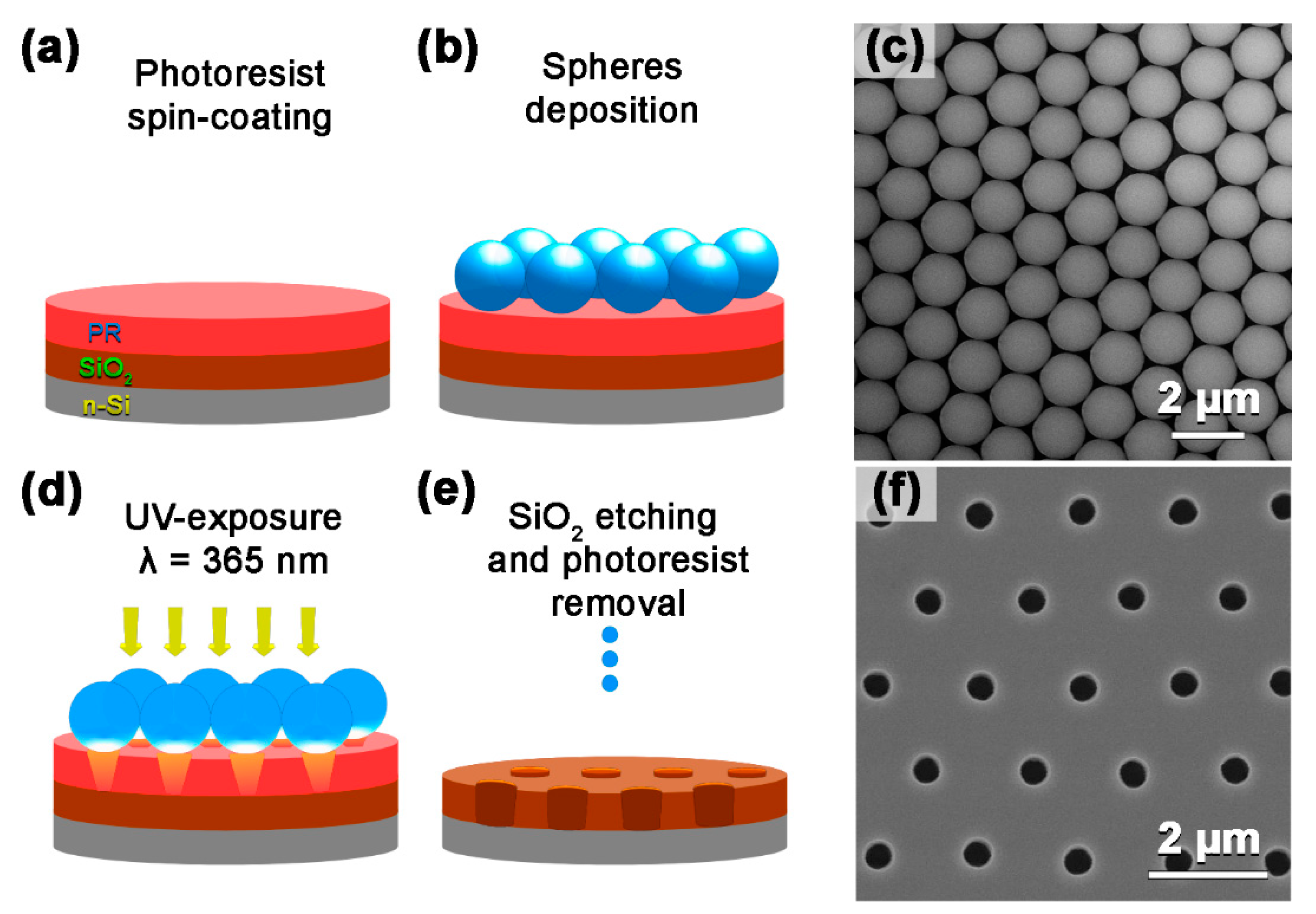
2.1. Si/SiO2 Substrate Patterning
2.2. MBE Growth
3. Results and Discussion
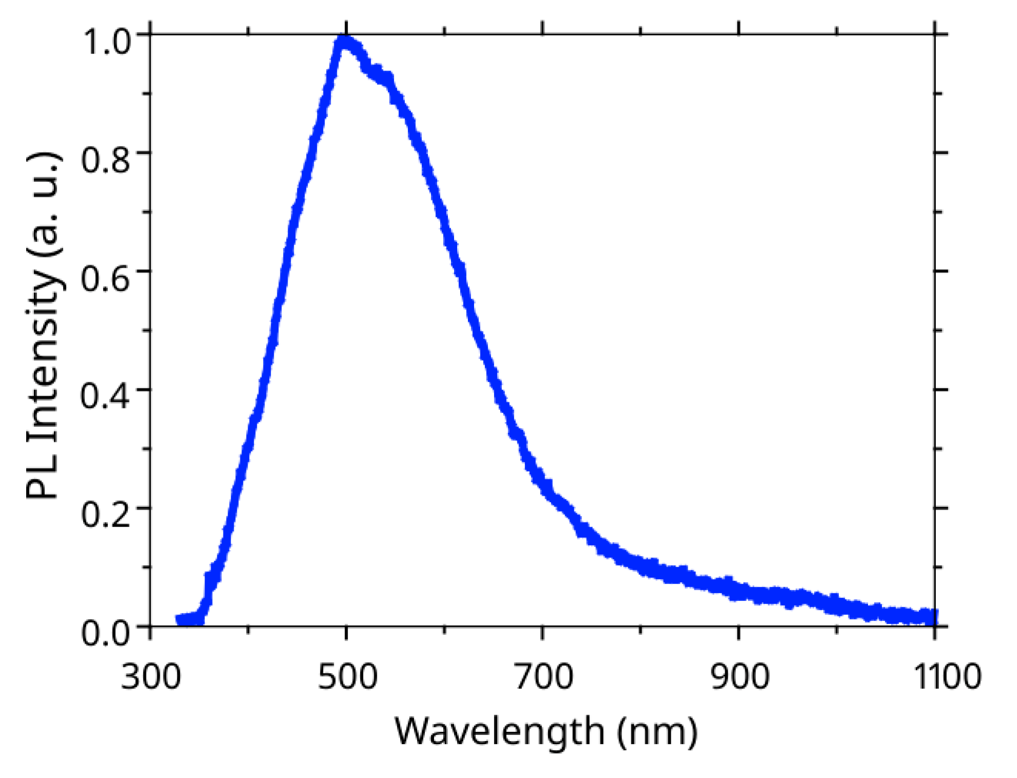
3.1. Optical Properties Study
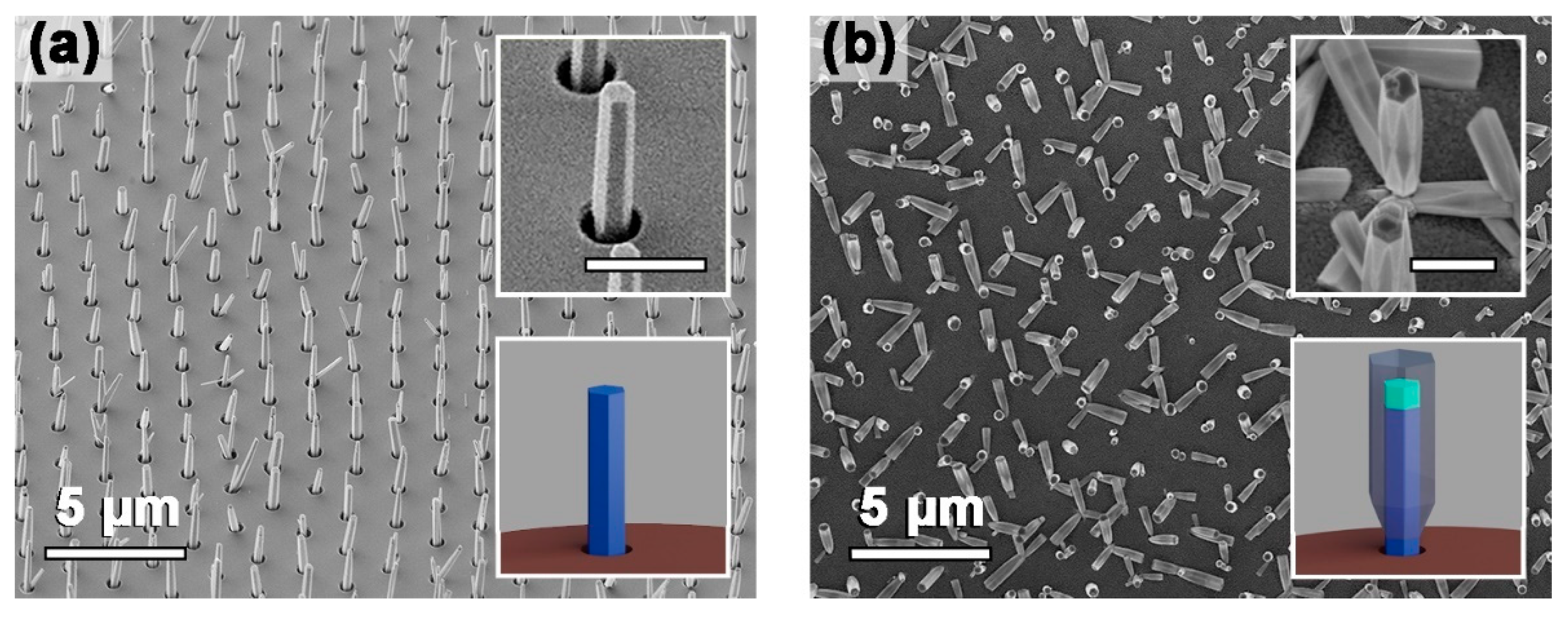
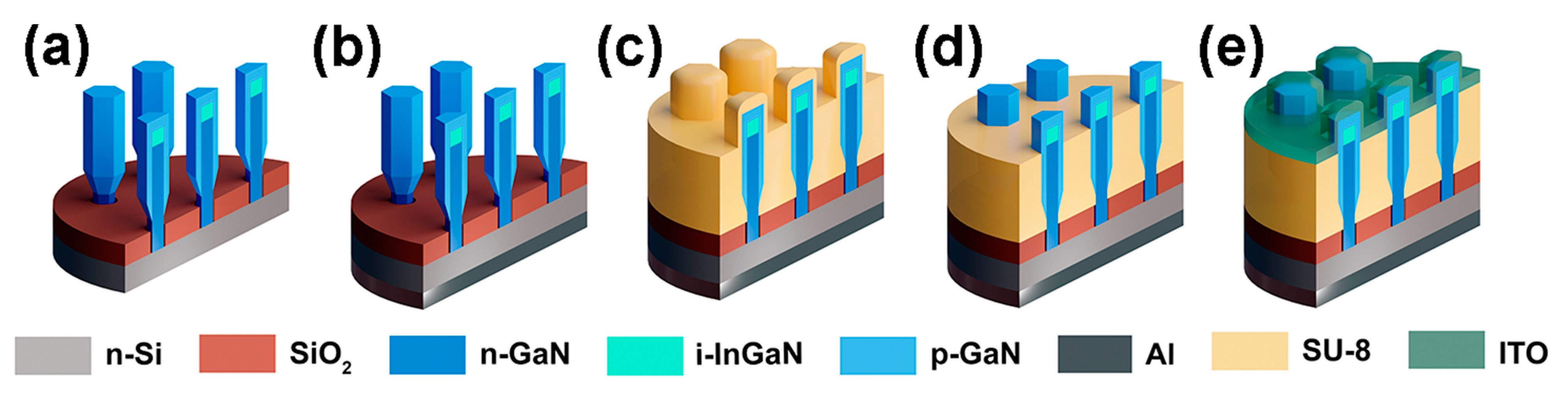
3.2. Device Processing
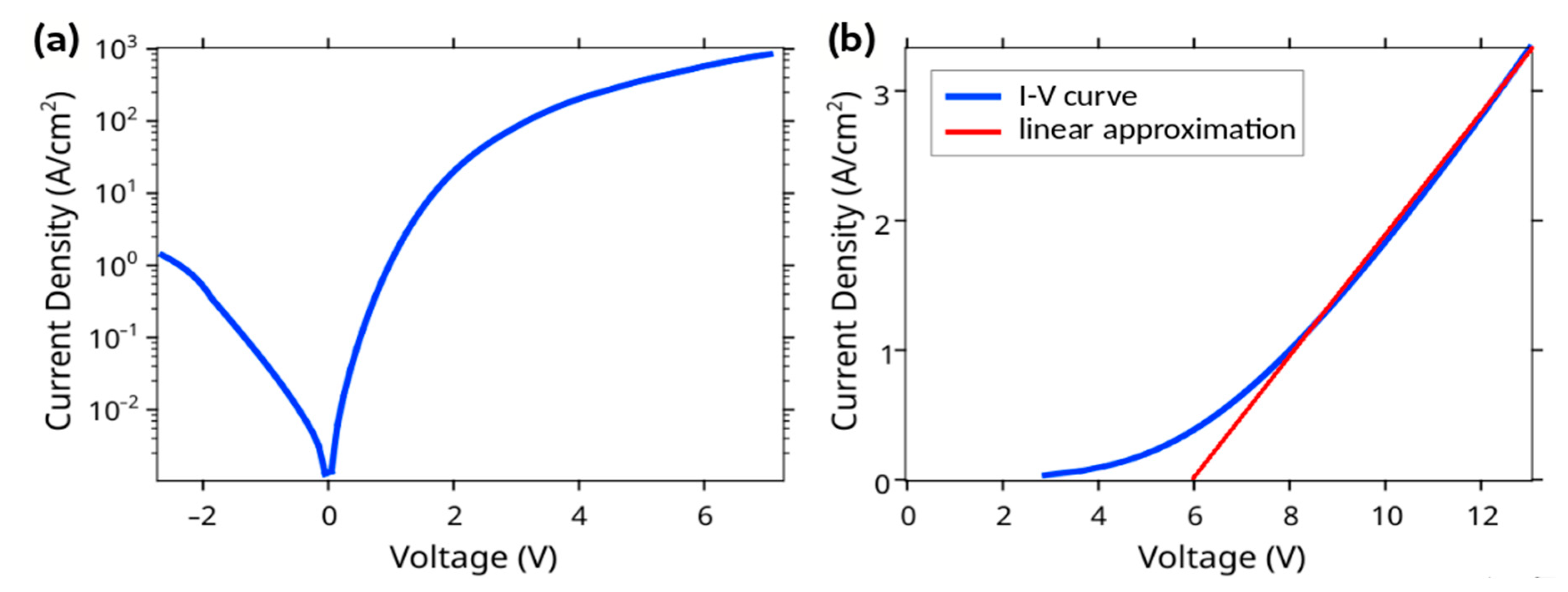
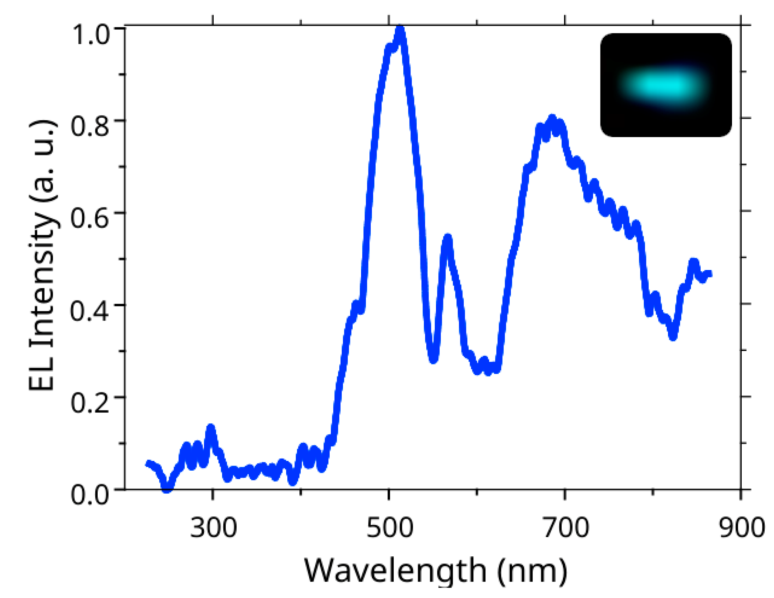
3.3. Electrical and Electroluminescent Characterization
4. Conclusions
Supplementary Materials
Author Contributions
Funding
Data Availability Statement
Conflicts of Interest
References
- Chen, C.-Y.; Zhu, G.; Hu, Y.; Yu, J.-W.; Song, J.; Cheng, K.-Y.; Peng, L.-H.; Chou, L.-J.; Wang, Z.L. Gallium nitride nanowire based nanogenerators and light-emitting diodes. ACS Nano 2012, 6, 5687–5692. [Google Scholar] [CrossRef] [PubMed]
- Tchernycheva, M.; Lavenus, P.; Zhang, H.; Babichev, A.V.; Jacopin, G.; Shahmohammadi, M.; Julien, F.H.; Ciechonski, R.; Vescovi, G.; Kryliouk, O. InGaN/GaN core–shell single nanowire light emitting diodes with graphene-based p-contact. Nano Lett. 2014, 14, 2456–2465. [Google Scholar] [CrossRef] [PubMed]
- Mozharov, A.; Bolshakov, A.; Cirlin, G.; Mukhin, I. Numerical modeling of photovoltaic efficiency of N-type GaN nanowires on p-Type Si heterojunction. Phys. Status Solidi RRL 2015, 9, 507–510. [Google Scholar] [CrossRef]
- Cirlin, G.E.; Dubrovskii, V.G.; Samsonenko, Y.B.; Bouravleuv, A.D.; Durose, K.; Proskuryakov, Y.Y.; Mendes, B.; Bowen, L.; Kaliteevski, M.A.; Abram, R.A.; et al. Self-catalyzed, pure zincblende GaAs nanowires grown on Si(111) by molecular beam epitaxy. Phys. Rev. B 2010, 82, 035302. [Google Scholar] [CrossRef] [Green Version]
- Songmuang, R.; Landré, O.; Daudin, B. From nucleation to growth of catalyst-free GaN nanowires on thin AlN buffer layer. Appl. Phys. Lett. 2007, 91, 251902. [Google Scholar] [CrossRef]
- Kuykendall, T.R.; Schwartzberg, A.M.; Aloni, S. Gallium nitride nanowires and heterostructures: Toward color-tunable and white-light sources. Adv. Mater. 2015, 27, 5805–5812. [Google Scholar] [CrossRef] [PubMed]
- Zhao, S.; Connie, A.T.; Dastjerdi, M.H.T.; Kong, X.H.; Wang, Q.; Djavid, M.; Sadaf, S.; Liu, X.D.; Shih, I.; Guo, H.; et al. Aluminum nitride nanowire light emitting diodes: Breaking the fundamental bottleneck of deep ultraviolet light sources. Sci. Rep. 2015, 5, 8332. [Google Scholar] [CrossRef]
- Zhao, C.; Alfaraj, N.; Subedi, R.C.; Liang, J.W.; Alatawi, A.A.; Alhamoud, A.A.; Ebaid, M.; Alias, M.S.; Ng, T.K.; Ooi, B.S. III-nitride nanowires on unconventional substrates: From materials to optoelectronic device applications. Prog. Quantum Electron. 2018, 61, 1–31. [Google Scholar] [CrossRef]
- Janjua, B.; Sun, H.; Zhao, C.; Anjum, D.H.; Priante, D.; Alhamoud, A.A.; Wu, F.; Li, X.; Albadri, A.M.; Alyamani, A.Y.; et al. Droop-free Al x Ga 1-x N/Al y Ga 1-y N quantum-disks-in-nanowires ultraviolet LED emitting at 337 Nm on metal/silicon substrates. Opt. Express 2017, 25, 1381–1390. [Google Scholar] [CrossRef]
- Janjua, B.; Sun, H.; Zhao, C.; Anjum, D.H.; Wu, F.; Alhamoud, A.A.; Li, X.; Albadri, A.M.; Alyamani, A.Y.; El-Desouki, M.M.; et al. Self-planarized quantum-disks-in-nanowires ultraviolet-B emitters utilizing pendeo-epitaxy. Nanoscale 2017, 9, 7805–7813. [Google Scholar] [CrossRef] [Green Version]
- Alfaraj, N.; Mitra, S.; Wu, F.; Ajia, I.A.; Janjua, B.; Prabaswara, A.; Aljefri, R.A.; Sun, H.; Khee Ng, T.; Ooi, B.S.; et al. Photoinduced entropy of InGaN/GaN p-i-n double-heterostructure nanowires. Appl. Phys. Lett. 2017, 110, 161110. [Google Scholar] [CrossRef] [Green Version]
- Sadaf, S.M.; Zhao, S.; Wu, Y.; Ra, Y.-H.; Liu, X.; Vanka, S.; Mi, Z. An AlGaN core–shell tunnel junction nanowire light-emitting diode operating in the ultraviolet-c band. Nano Lett. 2017, 17, 1212–1218. [Google Scholar] [CrossRef]
- Dai, X.; Messanvi, A.; Zhang, H.; Durand, C.; Eymery, J.; Bougerol, C.; Julien, F.H.; Tchernycheva, M. Flexible light-emitting diodes based on vertical nitride nanowires. Nano Lett. 2015, 15, 6958–6964. [Google Scholar] [CrossRef] [Green Version]
- Guo, W.; Zhang, M.; Banerjee, A.; Bhattacharya, P. Catalyst-free InGaN/GaN nanowire light emitting diodes grown on (001) silicon by molecular beam epitaxy. Nano Lett. 2010, 10, 3355–3359. [Google Scholar] [CrossRef]
- Limbach, F.; Hauswald, C.; Lähnemann, J.; Wölz, M.; Brandt, O.; Trampert, A.; Hanke, M.; Jahn, U.; Calarco, R.; Geelhaar, L.; et al. Current path in light emitting diodes based on nanowire ensembles. Nanotechnology 2012, 23, 465301. [Google Scholar] [CrossRef] [Green Version]
- Nguyen, H.P.T.; Zhang, S.; Connie, A.T.; Kibria, M.G.; Wang, Q.; Shih, I.; Mi, Z. Breaking the carrier injection bottleneck of phosphor-free nanowire white light-emitting diodes. Nano Lett. 2013, 13, 5437–5442. [Google Scholar] [CrossRef]
- Sree, V.G.; Bathula, C.; Kadam, A.N.; Ravindra, M.; Mahadevan, K.; Sohn, J.I.; Kim, H.-S.; Im, H. Halogen free solvent processed light-emitting diodes achieving EQE nearly 25% for imidazole-based host materials synthesized by ball milling. Nano Energy 2022, 92, 106753. [Google Scholar] [CrossRef]
- Roelkens, G.; Van Campenhout, J.; Brouckaert, J.; Van Thourhout, D.; Baets, R.; Romeo, P.R.; Regreny, P.; Kazmierczak, A.; Seassal, C.; Letartre, X.; et al. III-V/Si photonics by die-to-wafer bonding. Mater. Today 2007, 10, 36–43. [Google Scholar] [CrossRef]
- Fortuna, S.A.; Li, X. Metal-catalyzed semiconductor nanowires: A review on the control of growth directions. Semicond. Sci. Technol. 2010, 25, 024005. [Google Scholar] [CrossRef] [Green Version]
- Chèze, C.; Geelhaar, L.; Trampert, A.; Riechert, H. In situ investigation of self-induced GaN nanowire nucleation on Si. Appl. Phys. Lett. 2010, 97, 043101. [Google Scholar] [CrossRef] [Green Version]
- Bolshakov, A.D.; Fedorov, V.V.; Shugurov, K.Y.; Mozharov, A.M.; Sapunov, G.A.; Shtrom, I.V.; Mukhin, M.S.; Uvarov, A.V.; Cirlin, G.E.; Mukhin, I.S. Effects of the surface preparation and buffer layer on the morphology, electronic and optical properties of the GaN nanowires on Si. Nanotechnology 2019, 30, 395602. [Google Scholar] [CrossRef] [PubMed]
- Fedorov, V.V.; Bolshakov, A.D.; Kirilenko, D.A.; Mozharov, A.M.; Sitnikova, A.A.; Sapunov, G.A.; Dvoretckaia, L.N.; Shtrom, I.V.; Cirlin, G.E.; Mukhin, I.S. Droplet epitaxy mediated growth of GaN nanostructures on Si (111) via plasma-assisted molecular beam epitaxy. CrystEngComm 2018, 20, 3370–3380. [Google Scholar] [CrossRef]
- Bolshakov, A.D.; Mozharov, A.M.; Sapunov, G.A.; Shtrom, I.V.; Sibirev, N.V.; Fedorov, V.V.; Ubyivovk, E.V.; Tchernycheva, M.; Cirlin, G.E.; Mukhin, I.S. Dopant-stimulated growth of GaN nanotube-like nanostructures on Si(111) by molecular beam epitaxy. Beilstein J. Nanotechnol. 2018, 9, 146–154. [Google Scholar] [CrossRef] [PubMed]
- Yuan, X.; Pan, D.; Zhou, Y.; Zhang, X.; Peng, K.; Zhao, B.; Deng, M.; He, J.; Tan, H.H.; Jagadish, C. Selective area epitaxy of III–V nanostructure arrays and networks: Growth, applications, and future directions. Appl. Phys. Rev. 2021, 8, 021302. [Google Scholar] [CrossRef]
- Nami, M.; Stricklin, I.E.; DaVico, K.M.; Mishkat-Ul-Masabih, S.; Rishinaramangalam, A.K.; Brueck, S.R.J.; Brener, I.; Feezell, D.F. Carrier dynamics and electro-optical characterization of high-performance GaN/InGaN core-shell nanowire light-emitting diodes. Sci. Rep. 2018, 8, 501. [Google Scholar] [CrossRef] [Green Version]
- Demontis, V.; Zannier, V.; Sorba, L.; Rossella, F. Surface nano-patterning for the bottom-up growth of III-V semiconductor nanowire ordered arrays. Nanomaterials 2021, 11, 2079. [Google Scholar] [CrossRef]
- Yamazaki, K.; Yamaguchi, H. Three-dimensional alignment with 10nm order accuracy in electron-beam lithography on rotated sample for three-dimensional nanofabrication. J. Vac. Sci. Technol. B 2008, 26, 2529–2533. [Google Scholar] [CrossRef]
- Li, S.; Waag, A. GaN based nanorods for solid state lighting. J. Appl. Phys. 2012, 111, 071101. [Google Scholar] [CrossRef]
- Jeon, J.; Floresca, H.C.; Kim, M.J. Fabrication of complex three-dimensional nanostructures using focused ion beam and nanomanipulation. J. Vac. Sci. Technol. B Nanotechnol. Microelectron. Mater. Process. Meas. Phenom. 2010, 28, 549–553. [Google Scholar] [CrossRef]
- Zhang, Z.; Geng, C.; Hao, Z.; Wei, T.; Yan, Q. Recent advancement on micro-/nano-spherical lens photolithography based on monolayer colloidal crystals. Adv. Colloid Interface Sci. 2016, 228, 105–122. [Google Scholar] [CrossRef] [Green Version]
- García Núñez, C.; Navaraj, W.T.; Liu, F.; Shakthivel, D.; Dahiya, R. Large-area self-assembly of silica microspheres/nanospheres by temperature-assisted dip-coating. ACS Appl. Mater. Interfaces 2018, 10, 3058–3068. [Google Scholar] [CrossRef] [PubMed]
- Dvoretckaia, L.N.; Mozharov, A.M.; Berdnikov, Y.; Mukhin, I.S. Optimization of microsphere optical lithography for nano-patterning. J. Phys. D Appl. Phys. 2021, 55, 09LT01. [Google Scholar] [CrossRef]
- Gridchin, V.O.; Kotlyar, K.P.; Reznik, R.R.; Dvoretskaya, L.N.; Parfen’eva, A.V.; Mukhin, I.S.; Cirlin, G.E. Selective-area growth of GaN nanowires on patterned SiOx/Si substrates by molecular beam epitaxy. Tech. Phys. Lett. 2020, 46, 1080–1083. [Google Scholar] [CrossRef]
- Bolshakov, A.D.; Dvoretckaia, L.N.; Fedorov, V.V.; Sapunov, G.A.; Mozharov, A.M.; Shugurov, K.Y.; Shkoldin, V.A.; Mukhin, M.S.; Cirlin, G.E.; Mukhin, I.S. Microlens-enhanced substrate patterning and MBE growth of GaP nanowires. Semiconductors 2018, 52, 2088–2091. [Google Scholar] [CrossRef]
- Zhu, J.; Goddard, L.L. Spatial control of photonic nanojets. Opt. Express 2016, 24, 30444. [Google Scholar] [CrossRef]
- Kruse, J.E.; Lymperakis, L.; Eftychis, S.; Adikimenakis, A.; Doundoulakis, G.; Tsagaraki, K.; Androulidaki, M.; Olziersky, A.; Dimitrakis, P.; Ioannou-Sougleridis, V.; et al. Selective-area growth of GaN nanowires on SiO 2 -masked Si (111) substrates by molecular beam epitaxy. J. Appl. Phys. 2016, 119, 224305. [Google Scholar] [CrossRef]
- Schuster, F.; Hetzl, M.; Weiszer, S.; Garrido, J.A.; de la Mata, M.; Magen, C.; Arbiol, J.; Stutzmann, M. Position-controlled growth of GaN nanowires and nanotubes on diamond by molecular beam epitaxy. Nano Lett. 2015, 15, 1773–1779. [Google Scholar] [CrossRef] [Green Version]
- Ho, I.; Stringfellow, G.B. Solid phase immiscibility in GaInN. Appl. Phys. Lett. 1996, 69, 2701–2703. [Google Scholar] [CrossRef]
- Sawicka, M.; Feduniewicz-Żmuda, A.; Kryśko, M.; Turski, H.; Muziol, G.; Siekacz, M.; Wolny, P.; Skierbiszewski, C. Indium incorporation in semipolar (2021) and nonpolar (1010) InGaN grown by plasma assisted molecular beam epitaxy. J. Cryst. Growth 2017, 459, 129–134. [Google Scholar] [CrossRef]
Publisher’s Note: MDPI stays neutral with regard to jurisdictional claims in published maps and institutional affiliations. |
© 2022 by the authors. Licensee MDPI, Basel, Switzerland. This article is an open access article distributed under the terms and conditions of the Creative Commons Attribution (CC BY) license (https://creativecommons.org/licenses/by/4.0/).
Share and Cite
Dvoretckaia, L.; Gridchin, V.; Mozharov, A.; Maksimova, A.; Dragunova, A.; Melnichenko, I.; Mitin, D.; Vinogradov, A.; Mukhin, I.; Cirlin, G. Light-Emitting Diodes Based on InGaN/GaN Nanowires on Microsphere-Lithography-Patterned Si Substrates. Nanomaterials 2022, 12, 1993. https://doi.org/10.3390/nano12121993
Dvoretckaia L, Gridchin V, Mozharov A, Maksimova A, Dragunova A, Melnichenko I, Mitin D, Vinogradov A, Mukhin I, Cirlin G. Light-Emitting Diodes Based on InGaN/GaN Nanowires on Microsphere-Lithography-Patterned Si Substrates. Nanomaterials. 2022; 12(12):1993. https://doi.org/10.3390/nano12121993
Chicago/Turabian StyleDvoretckaia, Liliia, Vladislav Gridchin, Alexey Mozharov, Alina Maksimova, Anna Dragunova, Ivan Melnichenko, Dmitry Mitin, Alexandr Vinogradov, Ivan Mukhin, and Georgy Cirlin. 2022. "Light-Emitting Diodes Based on InGaN/GaN Nanowires on Microsphere-Lithography-Patterned Si Substrates" Nanomaterials 12, no. 12: 1993. https://doi.org/10.3390/nano12121993
APA StyleDvoretckaia, L., Gridchin, V., Mozharov, A., Maksimova, A., Dragunova, A., Melnichenko, I., Mitin, D., Vinogradov, A., Mukhin, I., & Cirlin, G. (2022). Light-Emitting Diodes Based on InGaN/GaN Nanowires on Microsphere-Lithography-Patterned Si Substrates. Nanomaterials, 12(12), 1993. https://doi.org/10.3390/nano12121993