
Optimal Energetic-Trap Distribution of Nano-Scaled Charge Trap Nitride for Wider Vth Window in 3D NAND Flash Using a Machine-Learning Method

 , , , , , ,
  , and
, and
Abstract
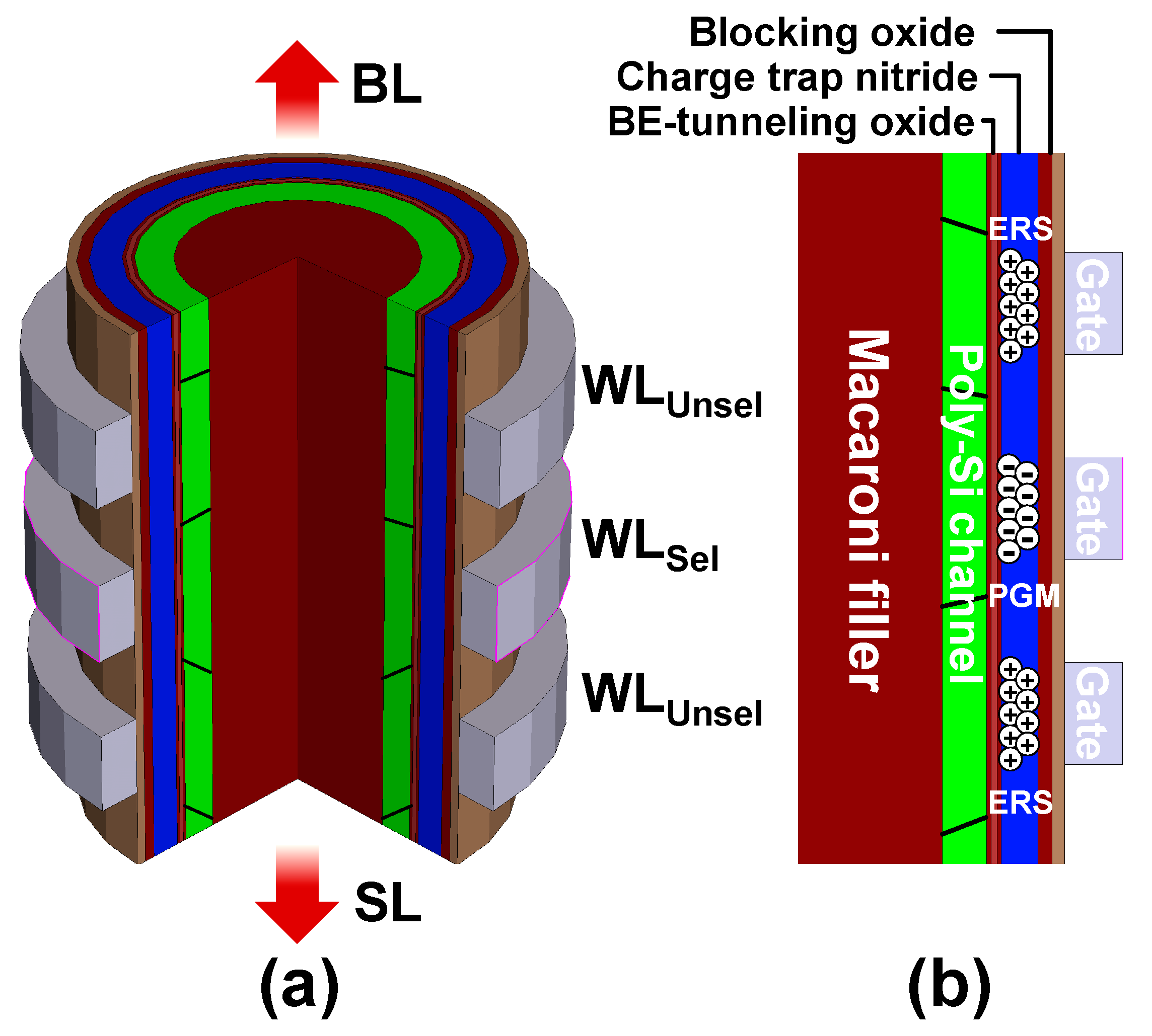
:1. Introduction
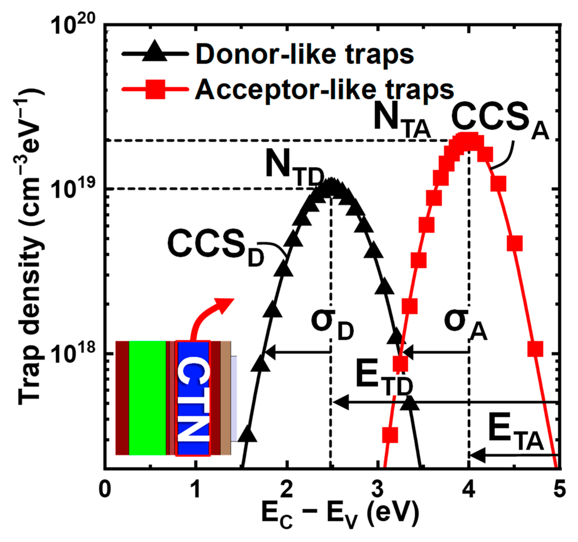
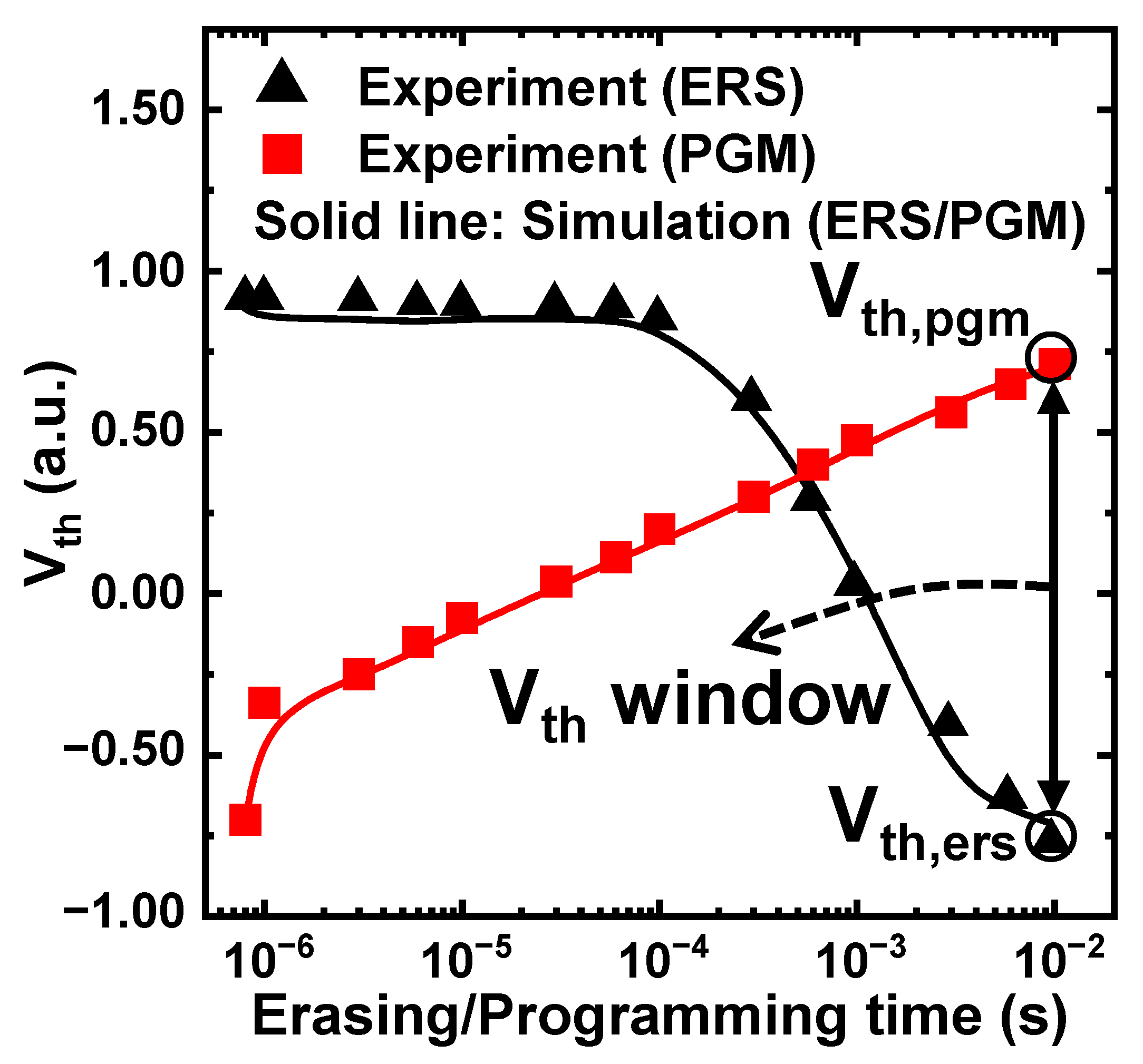
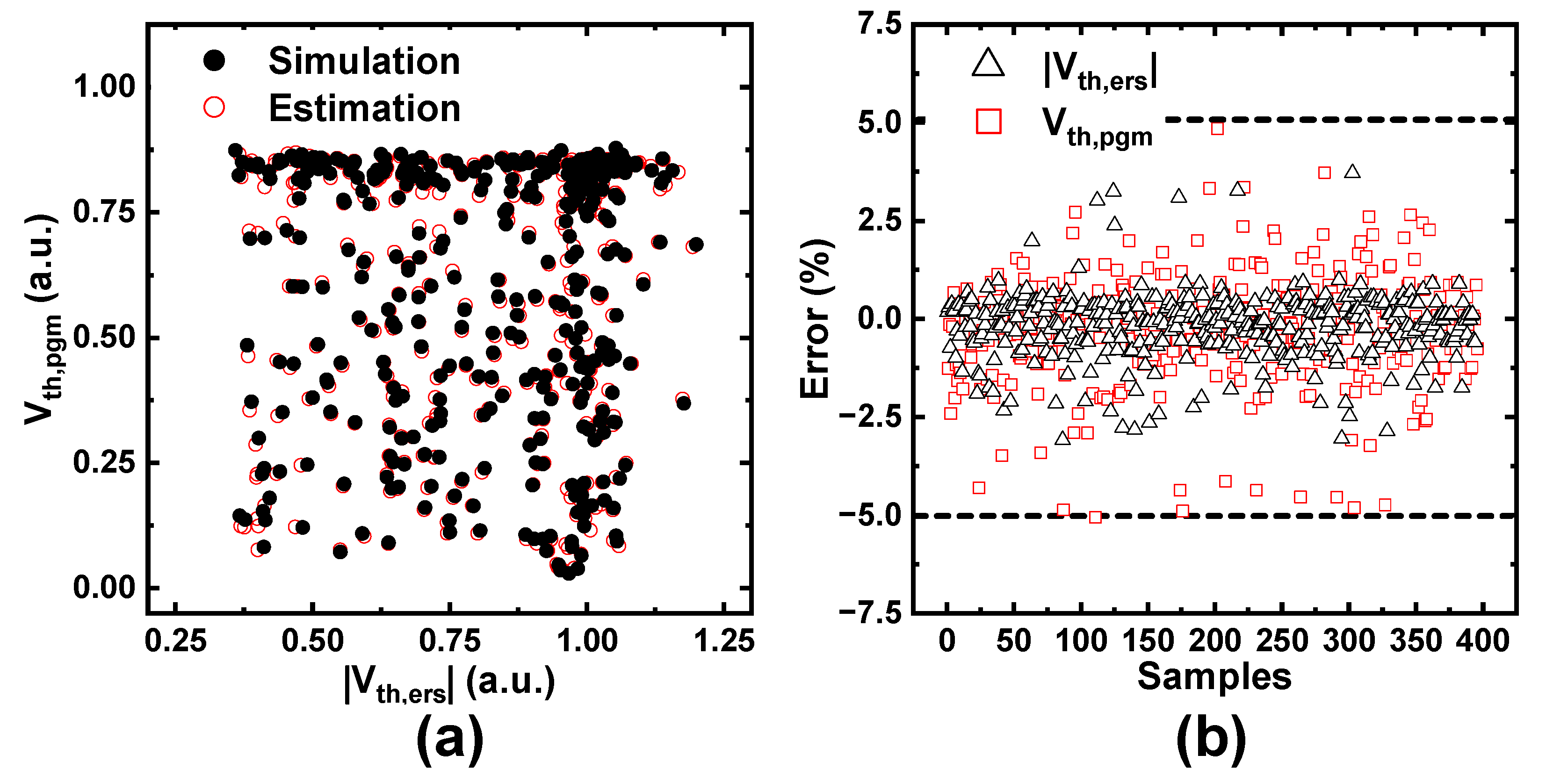
2. Simulation and Machine-Learning Method
3. Results and Discussion
4. Conclusions
Author Contributions
Funding
Data Availability Statement
Acknowledgments
Conflicts of Interest
References
- Ishimaru, K. Future of non-volatile memory from storage to computing. In Proceedings of the IEEE International Electron Device Meeting (IEDM), San Francisco, CA, USA, 5–8 December 2019; pp. 1.3.1–1.3.6. [Google Scholar] [CrossRef]
- Choi, E.-S.; Park, S.-K. Device considerations for high density and highly reliable 3D NAND Flash cell in near future. In Proceedings of the IEEE International Electron Device Meeting (IEDM), San Francisco, CA, USA, 5–7 December 2011; pp. 211–214. [Google Scholar] [CrossRef]
- Katsumata, R.; Kito, M.; Fukuzumi, Y.; Kido, M.; Tanaka, H.; Komori, Y.; Ishiduki, M.; Matsunami, J.; Fujiwara, T.; Nagata, Y.; et al. Pipe-shaped BiCS Flash memory with 16 stacked layers and multi-level-cell operation for ultra high density storage devices. In Proceedings of the Symposium on VLSI Technology, Kyoto, Japan, 15–17 June 2009; pp. 136–137. [Google Scholar]
- Jang, J.; Kim, H.-S.; Cho, W.; Cho, H.; Kim, J.; Shim, S.I.; Jang, Y.; Jeong, J.-H.; Son, B.-K.; Kim, D.W.; et al. Vertical cell array using TCAT(Terabit Cell Array Transistor) technology for ultra high density NAND Flash memory. In Proceedings of the Symposium on VLSI Technology, Kyoto, Japan, 15–17 June 2009; pp. 192–193. [Google Scholar]
- Tanaka, H.; Kido, M.; Yahashi, K.; Oomura, M.; Katsumata, R.; Kito, M.; Fukuzumi, Y.; Sato, M.; Nagata, Y.; Matsuoka, Y.; et al. Bit cost scalable technology with punch and plug process for ultra high density Flash memory. In Proceedings of the Symposium on VLSI Technology, Kyoto, Japan, 12–14 June 2007; pp. 14–15. [Google Scholar] [CrossRef]
- Lee, S.; Lee, Y.-T.; Han, W.-K.; Kim, D.-H.; Kim, M.-S.; Moon, S.-H.; Cho, H.C.; Lee, J.-W.; Byeon, D.-S.; Lim, Y.-H.; et al. A 3.3 V 4 Gb four-level NAND Flash memory with 90 nm CMOS technology. In Proceedings of the IEEE International Solid-State Circuits Conference (ISSCC), San Francisco, CA, USA, 15–19 February 2004; pp. 52–53. [Google Scholar] [CrossRef]
- Lee, S.; Kim, C.; Kim, M.; Joe, S.-M.; Jang, J.; Kim, S.; Lee, K.; Kim, J.; Park, J.; Lee, H.-J.; et al. A 1Tb 4b/Cell 64-Stacked-W 3D NAND Flash memory with 12MB/s program throughput. In Proceedings of the IEEE International Solid-State Circuits Conference (ISSCC), San Francisco, CA, USA, 11–15 February 2018; pp. 340–342. [Google Scholar] [CrossRef]
- Shibata, N.; Kanda, K.; Shimizu, T.; Nakai, J.; Nagao, O.; Kobayashi, N.; Miakashi, M.; Nagadomi, Y.; Nakano, T.; Kawabe, T.; et al. A 1.33-Tb 4-bit/cell 3-D Flash memory on a 96-word-line-layer technology. IEEE J. Solid-State Circuits 2020, 55, 178–188. [Google Scholar] [CrossRef]
- Mizoguchi, K.; Takahashi, T.; Aritome, S.; Takeuchi, K. Data retention characteristics comparison of 2D and 3D TLC NAND Flash memories. In Proceedings of the IEEE Memory Workshop (IMW), Monterey, CA, USA, 14–17 May 2017; pp. 1–4. [Google Scholar] [CrossRef]
- Shibata, N.; Maejima, H.; Isobe, K.; Iwasa, K.; Nakagawa, M.; Fujiu, M.; Shimizu, T.; Honma, M.; Hoshi, S.; Kawaai, T.; et al. A 70 nm 16 Gb 16-level-cell NAND Flash memory. IEEE J. Solid-State Circuits 2008, 43, 929–937. [Google Scholar] [CrossRef]
- Cai, Y.; Luo, Y.; Ghose, S.; Mutlu, O. Read disturb errors in MLC NAND Flash memory: Characterization, mitigation, and recovery. In Proceedings of the 45th Annual IEEE/IFIP International Conference on Dependable Systems and Networks, Rio de Janeiro, Brazil, 22–25 June 2015; pp. 438–449. [Google Scholar] [CrossRef] [Green Version]
- Parat, K.; Goda, A. Scaling trends in NAND Flash. In Proceedings of the IEEE International Electron Device Meeting (IEDM), San Francisco, CA, USA, 1–5 December 2018; pp. 2.1.1–2.1.4. [Google Scholar] [CrossRef]
- Yoon, C.-W.; Kim, H.-G.; Lee, S.-K.; Lee, J.; Song, J.H. Issues and key technologies for next generation 3D NAND. In Proceedings of the International Conference on Electronics, Information, and Communication (ICEIC), Jeju, Korea, 31 January–3 February 2021; pp. 1–4. [Google Scholar] [CrossRef]
- Shin, Y.; Choi, J.; Kang, C.; Lee, C.; Park, K.-T.; Lee, J.-S.; Sel, J.; Kim, V.; Choi, B.; Sim, J.; et al. A novel NAND-type MONOS memory using 63nm process technology for multi-gigabit flash EEPROMs. In Proceedings of the IEEE International Electron Device Meeting (IEDM), Washington, DC, USA, 5–7 December 2005; pp. 327–330. [Google Scholar] [CrossRef]
- Lee, C.-H.; Choi, J.; Kang, C.; Shin, Y.; Lee, J.-S.; Sel, J.; Sim, J.; Jeon, S.; Choe, B.-I.; Bae, D.; et al. Multi-level NAND flash memory with 63 nm-node TANOS (Si-Oxide-SiN-Al2O3-TaN) cell structure. In Proceedings of the Symposium on VLSI Technology, Honolulu, HI, USA, 13–15 June 2006; pp. 21–22. [Google Scholar] [CrossRef]
- Yang, Y.; White, M.H. Charge retention of scaled SONOS non-volatile memory devices at elevated temperatures. Solid-State Electron. 2000, 44, 949–958. [Google Scholar] [CrossRef]
- Kang, H.-J.; Choi, N.; Joe, S.-M.; Seo, J.-H.; Choi, E.; Park, S.-K.; Park, B.-G.; Lee, J.-H. Comprehensive analysis of retention characteristics in 3-D NAND Flash memory cells with tube-type poly-Si channel structure. In Proceedings of the Symposium on VLSI Technology, Kyoto, Japan, 27 August 2015; pp. T182–T183. [Google Scholar] [CrossRef]
- Degraeve, R.; Cho, M.; Govoreanu, B.; Kaczer, B.; Zahid, M.B.; Van Houdt, J.; Jurczak, M.; Groeseneken, G. Trap spectroscopy by injection and sensing (TSCIS): A quantitative electrical technique for studying defects in dielectric stacks. In Proceedings of the IEEE International Electron Device Meeting (IEDM), San Francisco, CA, USA, 15–17 December 2008; pp. 1–4. [Google Scholar] [CrossRef]
- Kim, T.H.; Park, I.H.; Lee, J.D.; Shin, H.C.; Park, B.-G. Electron trap density distribution of Si-rich silicon nitride extracted using the modified negative charge decay model of silicon-oxide-nitride-oxide-silicon structure at elevated temperatures. Appl. Phys. Lett. 2006, 89, 063508. [Google Scholar] [CrossRef]
- Suhane, A.; Arreghini, A.; Degraeve, R.; Van den bosch, G.; Breuil, L.; Zahid, M.B.; Jurczak, M.; De Meyer, K.; Van Houdt, J. Validation of retention modeling as a trap-profiling technique for SiN-Based charge-trapping memories. IEEE Electron Device Lett. 2010, 31, 77–79. [Google Scholar] [CrossRef]
- Choi, E.-S.; Yoo, H.-S.; Park, K.-H.; Kim, S.-J.; Ahn, J.-R.; Lee, M.-S.; Hong, Y.-O.; Kim, S.-G.; Om, J.-C.; Joo, M.-S.; et al. Modeling and characterization of program/erasure speed and retention of TiN-gate MANOS (Si-Oxide-SiNx-Al2O3-Metal gate) cells for NAND Flash memory. In Proceedings of the IEEE Non-Volatile Semiconductor Memory Workshop (NVSMW), Monterey, CA, USA, 26–30 August 2007; pp. 83–84. [Google Scholar] [CrossRef]
- Choi, H.-C.; Yun, H.; Yoon, J.-S.; Baek, R.-H. Neural approach for modeling and optimizing Si-MOSFET manufacturing. IEEE Access 2020, 8, 159351–159370. [Google Scholar] [CrossRef]
- Yun, H.; Yoon, J.-S.; Jeong, J.; Lee, S.; Choi, H.-C.; Baek, R.-H. Neural network based design optimization of 14-nm node fully-depleted SOI FET for SoC and 3DIC applications. IEEE J. Electron Devices Soc. 2020, 8, 1272–1280. [Google Scholar] [CrossRef]
- Yoon, J.-S.; Lee, S.; Yun, H.; Baek, R.-H. Digital/Analog performance optimization of vertical nanowire FETs using machine learning. IEEE Access 2021, 9, 29071–29077. [Google Scholar] [CrossRef]
- Schmidhuber, J. Deep learning in neural networks: An overview. Neural Netw. 2015, 61, 85–117. [Google Scholar] [CrossRef] [PubMed] [Green Version]
- Sentaurus Device User Guide; Version: O-2018.06-SP2; Synopsys, Inc.: Mountain View, CA, USA, 2018.
- Nam, K.; Park, C.; Yoon, J.-S.; Jang, H.; Park, M.S.; Sim, J.; Baek, R.-H. Origin of incremental step pulse programming (ISPP) slope degradation in charge trap nitride base multi-layer 3D NAND Flash. Solid-State Electron. 2021, 175, 1–6. [Google Scholar] [CrossRef]
- Funahashi, K.-I. On the approximate realization of continuous mappings by neural networks. Neural Netw. 1989, 2, 183–192. [Google Scholar] [CrossRef]
- MATLAB User Manual; Version: R2019b; MathWorks, Inc.: Natick, MA, USA, 2019.
- Gritsenko, V.A.; Nekrashevich, S.S.; Vasilev, V.V.; Shaposhnikov, A.V. Electronic structure of memory traps in silicon nitride. Microelectron. Eng. 2009, 86, 1866–1869. [Google Scholar] [CrossRef]
- Vishnyakov, A.V.; Novikov, Y.N.; Gritsenko, V.A.; Nasyrov, K.A. The charge transport mechanism in silicon nitride: Multi-phonon trap ionization. Solid-State Electron. 2009, 53, 251–255. [Google Scholar] [CrossRef]


| Trap Parameter | Min | Max | Calibrated |
|---|---|---|---|
| Density of donor-like traps, NTD (cm−3·eV−1) | 5.00 × 10¹⁸ | 5.00 × 10¹⁹ | 1.00 × 10¹⁹ |
| Peak energy level of donor-like traps, ETD (eV) | 2.00 | 3.00 | 2.50 |
| Capture cross section of donor-like traps, CCSD (cm2) | 1.00 × 10⁻¹⁵ | 1.00 × 10⁻¹¹ | 1.00 × 10⁻¹³ |
| Standard deviation of donor-like traps, σD (eV) | 0.10 | 0.50 | 0.35 |
| Density of acceptor-like traps, NTA (cm−3·eV−1) | 8.00 × 10¹⁸ | 8.00 × 10¹⁹ | 2.00 × 10¹⁹ |
| Peak energy level of acceptor-like traps, ETA (eV) | 0.80 | 1.50 | 1.00 |
| Capture cross section of acceptor-like traps, CCSA (cm2) | 1.00 × 10⁻¹⁵ | 1.00 × 10⁻¹¹ | 1.00 × 10⁻¹³ |
| Standard deviation of acceptor-like traps, σA (eV) | 0.10 | 0.50 | 0.30 |
| Trap Parameter | Value |
|---|---|
| NTD (cm−3·eV−1) | 5.00 × 10¹⁹ |
| ETD (eV) | 2.00 |
| CCSD (cm2) | 1.00 × 10⁻¹⁵ |
| σD (eV) | 0.50 |
| NTA (cm−3·eV−1) | 8.00 × 10¹⁹ |
| ETA (eV) | 1.45 |
| CCSA (cm2) | 1.00 × 10⁻¹⁵ |
| σA (eV) | 0.50 |
Publisher’s Note: MDPI stays neutral with regard to jurisdictional claims in published maps and institutional affiliations. |
© 2022 by the authors. Licensee MDPI, Basel, Switzerland. This article is an open access article distributed under the terms and conditions of the Creative Commons Attribution (CC BY) license (https://creativecommons.org/licenses/by/4.0/).
Share and Cite
Nam, K.; Park, C.; Yoon, J.-S.; Yun, H.; Jang, H.; Cho, K.; Kang, H.-J.; Park, M.-S.; Sim, J.; Choi, H.-C.; et al. Optimal Energetic-Trap Distribution of Nano-Scaled Charge Trap Nitride for Wider Vth Window in 3D NAND Flash Using a Machine-Learning Method. Nanomaterials 2022, 12, 1808. https://doi.org/10.3390/nano12111808
Nam K, Park C, Yoon J-S, Yun H, Jang H, Cho K, Kang H-J, Park M-S, Sim J, Choi H-C, et al. Optimal Energetic-Trap Distribution of Nano-Scaled Charge Trap Nitride for Wider Vth Window in 3D NAND Flash Using a Machine-Learning Method. Nanomaterials. 2022; 12(11):1808. https://doi.org/10.3390/nano12111808
Chicago/Turabian StyleNam, Kihoon, Chanyang Park, Jun-Sik Yoon, Hyeok Yun, Hyundong Jang, Kyeongrae Cho, Ho-Jung Kang, Min-Sang Park, Jaesung Sim, Hyun-Chul Choi, and et al. 2022. "Optimal Energetic-Trap Distribution of Nano-Scaled Charge Trap Nitride for Wider Vth Window in 3D NAND Flash Using a Machine-Learning Method" Nanomaterials 12, no. 11: 1808. https://doi.org/10.3390/nano12111808
APA StyleNam, K., Park, C., Yoon, J.-S., Yun, H., Jang, H., Cho, K., Kang, H.-J., Park, M.-S., Sim, J., Choi, H.-C., & Baek, R.-H. (2022). Optimal Energetic-Trap Distribution of Nano-Scaled Charge Trap Nitride for Wider Vth Window in 3D NAND Flash Using a Machine-Learning Method. Nanomaterials, 12(11), 1808. https://doi.org/10.3390/nano12111808