Article

Novel Modeling Approach to Analyze Threshold Voltage Variability in Short Gate-Length (15–22 nm) Nanowire FETs with Various Channel Diameters

The Department of Electrical Engineering, Pohang University of Science and Technology (POSTECH), Pohang 37673, Gyeongbuk, Korea
*
Author to whom correspondence should be addressed.
Nanomaterials 2022, 12(10), 1721; https://doi.org/10.3390/nano12101721
Submission received: 1 April 2022 / Revised: 13 May 2022 / Accepted: 16 May 2022 / Published: 18 May 2022

Abstract

:
In this study, threshold voltage (Vth) variability was investigated in silicon nanowire field-effect transistors (SNWFETs) with short gate-lengths of 15–22 nm and various channel diameters (DNW) of 7, 9, and 12 nm. Linear slope and nonzero y-intercept were observed in a Pelgrom plot of the standard deviation of VthVth), which originated from random and process variations. Interestingly, the slope and y-intercept differed for each DNW, and σVth was the smallest at a median DNW of 9 nm. To analyze the observed DNW tendency of σVth, a novel modeling approach based on the error propagation law was proposed. The contribution of gate-metal work function, channel dopant concentration (Nch), and DNW variations (WFV, ∆Nch, and ∆DNW) to σVth were evaluated by directly fitting the developed model to measured σVth. As a result, WFV induced by metal gate granularity increased as channel area increases, and the slope of WFV in Pelgrom plot is similar to that of σVth. As DNW decreased, SNWFETs became robust to ∆Nch but vulnerable to ∆DNW. Consequently, the contribution of ∆DNW, WFV, and ∆Nch is dominant at DNW of 7 nm, 9 nm, and 12, respectively. The proposed model enables the quantifying of the contribution of various variation sources of Vth variation, and it is applicable to all SNWFETs with various LG and DNW.

1. Introduction

Gate-all-around (GAA) silicon nanowire field-effect transistors (SNWFETs) are considered as a viable option for future device architecture due to their adequate gate-controllability with GAA structures [1,2,3]. However, ultrascaled SNWFETs suffer from severe threshold voltage (Vth) variation because the device-to-device variation increases with the decrease in the effective channel width (Weff) and gate-length (LG) [4,5]. According to previous studies, random variations such as metal gate granularity (MGG), line edge roughness (LER), and random dopant fluctuation (RDF) cause Vth variation in ultrascaled GAA transistors [6,7,8,9,10]. Additionally, the Vth variation is also induced by the process variations such as junction gradient and channel thickness variation [11,12,13,14,15,16,17].
Therefore, several simulations and models have been recommended to analyze the contribution of multiple sources to Vth variation. First, technology computer-aided design (TCAD) simulations are suitable for analyzing the influence of variation sources, but it is difficult to predict the cause of variation inversely from measured Vth variation [6,7,8,9,10]. Second, simulation program with integrated circuit emphasis (SPICE)-based models can be applied to analyze the variation sources of measured Vth variation, but it consumes time and makes an error because all devices should be calibrated [15]. Last, models based on the error propagation law have been proposed [16,17]. These modeling approaches enable extraction of the contribution of each variation source to the standard deviation of VthVth) fast and accurately because they directly model σVth. However, the error propagation law-based model to analyze the Vth variability of SNWFET has not been suggested.
Previously, Vth variability in SNWFETs was investigated considering various LG using a SPICE-based model [15]. However, the study did not consider the effect of channel dopant concentration (Nch) variation and nanowire diameter (DNW) change. Furthermore, although DNW influences Weff, electrostatics, and quantum effect [18], the DNW tendency of Vth variability in SNWFET with short LG has not been thoroughly investigated.
Therefore, in this study, we quantitatively analyzed the sources of Vth variation in SNWFETs with short LG (15–22 nm) and multiple DNW (7, 9, 12 nm). A novel modeling approach based on the error propagation law is proposed to estimate the contribution of multiple variation sources to the Vth variability. The dominant variation source of Vth variation is analyzed for each DNW by using the proposed model. Additionally, the standard deviation of NchNch) and DNWDNW) according to LG is presented.

2. Device Structure and Modeling Methods

2.1. Structure and Possible Vth Variation Sources of SNWFETs

Figure 1 depicts the schematic and Vth variation sources of SNWFETs, fabricated using the same process flow reported in [19,20]. The SNWFETs adopted Mid-gap TiN metal gate, gate oxide thickness (tox) of 3.4 nm, and (110) channel direction. The gate and nanowire trimming process was used to obtain LG varying from 15 to 22 nm and DNW of 7, 9, and 12 nm. In this process, DNW variation (∆DNW) was caused by LER occurred at the nanowire (NW) edges and under- or over-etching of the NW [21]. MGG occurred in the TiN metal gate and generated the metal work function variation (WFV) [22]. The transmission electron microscope (TEM) image shows many grain boundaries exist in the TiN metal gate of the SNWFETs [19]. Although the SNWFET is fabricated with an undoped channel, the source/drain (S/D) dopants diffuse into the channel with short LG [18,23]. Consequently, Nch variation (∆Nch) was caused by RDF, the S/D dopant implant, annealing, and SiGe strain variation [8,9,10].
Figure 2a depicts the IDVG characteristics of SNWFETs with LG = 15 nm and DNW = 7 nm at a drain bias of 0.05 V. About 50 samples were measured per device condition. Here, Vth was extracted at ID = 10−7 × πDNW/LG using the constant current method. The fluctuation of extracted Vth shows the process and random variation affect the physical characteristics of SNWFETs. Figure 2b illustrates a quantile plot of Vth for each DNW in SNWFETs with an LG of 15 nm, which shows the distribution of Vth. The distribution of Vth predominantly follows the theoretical normal distribution for all device conditions, which indicates that sufficient Vth values were obtained to analyze σVth.
Figure 3 is the Pelgrom plot of σVth in SNWFETs for each DNW, showing the trend of σVth as channel area changes. The slope of the Pelgrom plot, defined as the Pelgrom coefficient (Avt), represents the effect of random variation [4]. The y-intercept of the Pelgrom plot is also observed, indicating the effect of the process variation and short channel effect [12,24]. Remarkably, the values of Avt and y-intercepts differed for each DNW, and the σVth is smallest in median DNW of 9 nm. We anticipated that this result implies a trade-off relationship between the various variation sources. Hence, a novel modeling approach is proposed to analyze the contribution of each variation source to σVth.

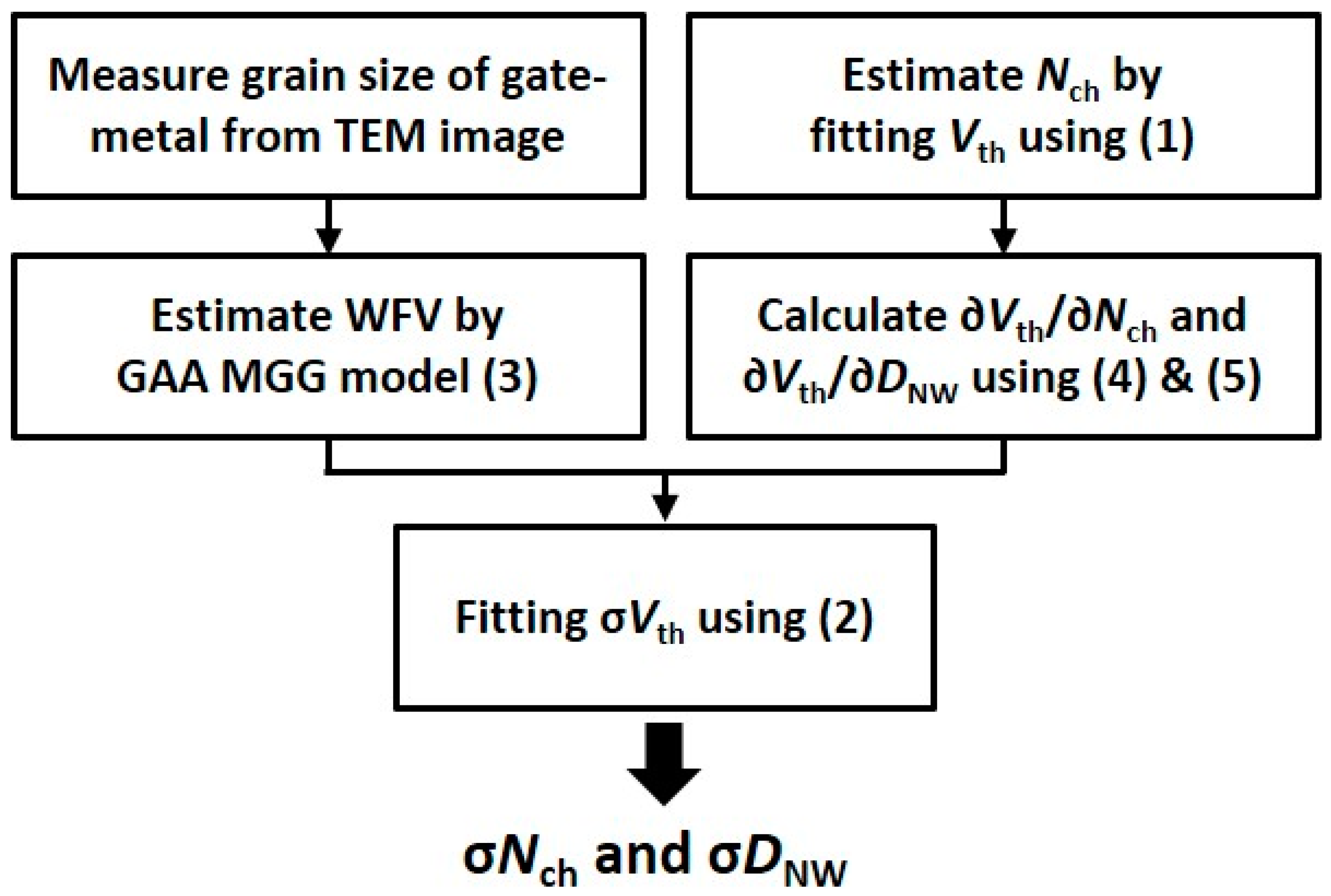
2.2. Proposed σVth Model of SNWFETs

Figure 4 shows the proposed modeling flow to analyze the contribution of WFV, ∆Nch, and ∆DNW to σVth. To model σVth, we started from a physical model for Vth of SNWFET, as follows [25,26]:
V th = Φ M Φ S q N ch ( π r nw 2 C ox + r nw 2 4 ε si ) + h 2 4 π m q r nw 2 ,
where ΦM denotes the work function of the TiN gate metal; ΦS represents the work function of silicon channel calculated as χsiEg/2 + kT/q∙ln(Nch/ni), where χsi is the electron affinity and Eg is the band gap of silicon; rnw indicates the radius of NW; ε si and ε ox represent the dielectric constant of silicon and oxide, respectively; h denotes the Planck constant; and m* indicates the effective mass of an electron. Cox represents the oxide capacitance calculated as 2πεox/ln(1 + tox/rnw). The possible Vth variation sources in Equation (1) are ΦM, Nch, DNW, and tox variations. Among them, tox is not considered because its variation and effect are very small and negligible [11,12,27]. Although the variation of effective channel length (Leff) is not considered directly, Nch variation partially represents Leff variation because S/D dopant diffusion and LG variation change Nch and Leff simultaneously.
Hence, considering three identical variation sources of WFV, ∆Nch, and ∆DNW, σVth can be expressed based on the error propagation law as
σ V th 2 = σ Φ M 2 + ( V th N ch · σ N ch ) 2 + ( V th D NW · σ D NW ) 2 .
To analyze σVth using Equation (2), the sensitivity of Vth against variation sources and their standard deviation should be extracted. First, the standard deviation of metal work function (σΦM) can be estimated by the existing WFV model for SNWFETs, as follows [22]:
σ Φ M = R G G × S L = G size L G ( D NW + 2 t ox ) π × S L ,
where RGG is the ratio of average grain size to the gate area, SL is the sensitivity of σVth against RGG, and Gsize is the grain size of the metal gate. Here, Gsize can be estimated from a TEM image of the TiN metal gate of SNWFETs. SL of SNWFETs can be obtained from previous research based on TCAD simulation [22].
Second, the sensitivity of Vth against ∆Nch and ∆DNW can be obtained by calculating the partial differentiation of Equation (1), as follows:
V th N ch = k T / q N ch q r nw 2 ( ln ( 1 + t ox / r nw ) 2 ε ox + 1 4 ε si ) ,
V th D NW = q N ch r nw 2 ( 1 ε ox ( 2 ln ( 1 + t ox r nw ) t ox t ox + r nw ) + 1 ε si ) h 2 2 π m q r nw 3 ,
where k denotes the Boltzmann constant. Here, Nch can be extracted where Equation (1) best fits to measured Vth. Finally, σNch and σDNW are extracted when Equation (2) best fits the square of the measured σVth.
The proposed model obtains the Vth sensitivity against ∆Nch and ∆DNW through simple calculation and extracts the standard deviation of each variation source by fitting the model to the measured σVth. Therefore, the contribution of multiple variation sources to σVth can be directly and quickly modeled and analyzed using the proposed model without any TCAD or SPICE simulation. Furthermore, the proposed Vth modeling flow is expected to be applied to analyze σVth in most multigate devices with various LG and channel thicknesses.

3. Results and Discussion

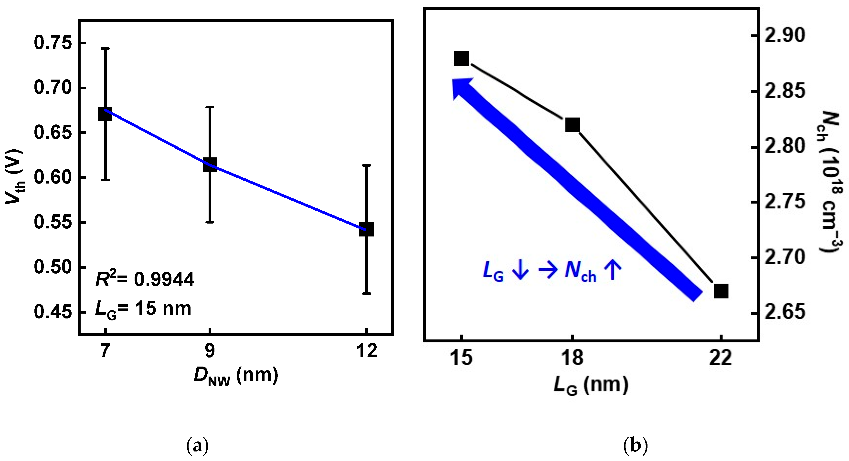
3.1. Vth Modeling Results of SNWFETs

Nch is extracted where Equation (1) fitted Vth versus DNW with high accuracy in SNWFET with LG of 15 nm, as shown in Figure 5a. Figure 5b shows Nch increases as LG decreases because more dopant diffused to the center of the channel from S/D even with the same S/D junction gradient. The sensitivity of Vth against ∆Nch and ∆DNW was calculated by substituting Nch and other parameters in Equations (4) and (5).

3.2. Vth Standard Deviation Modeling Results of SNWFETs

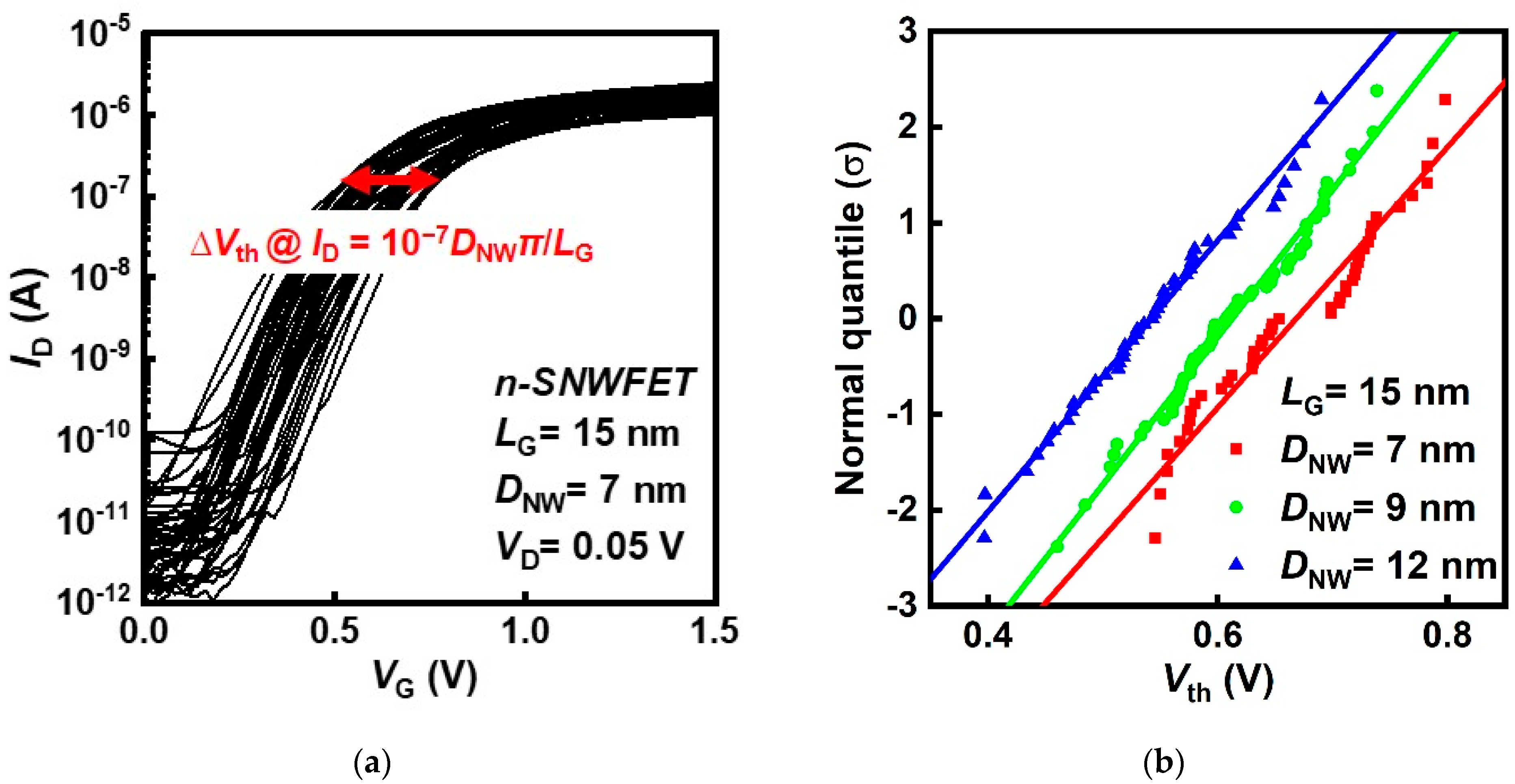
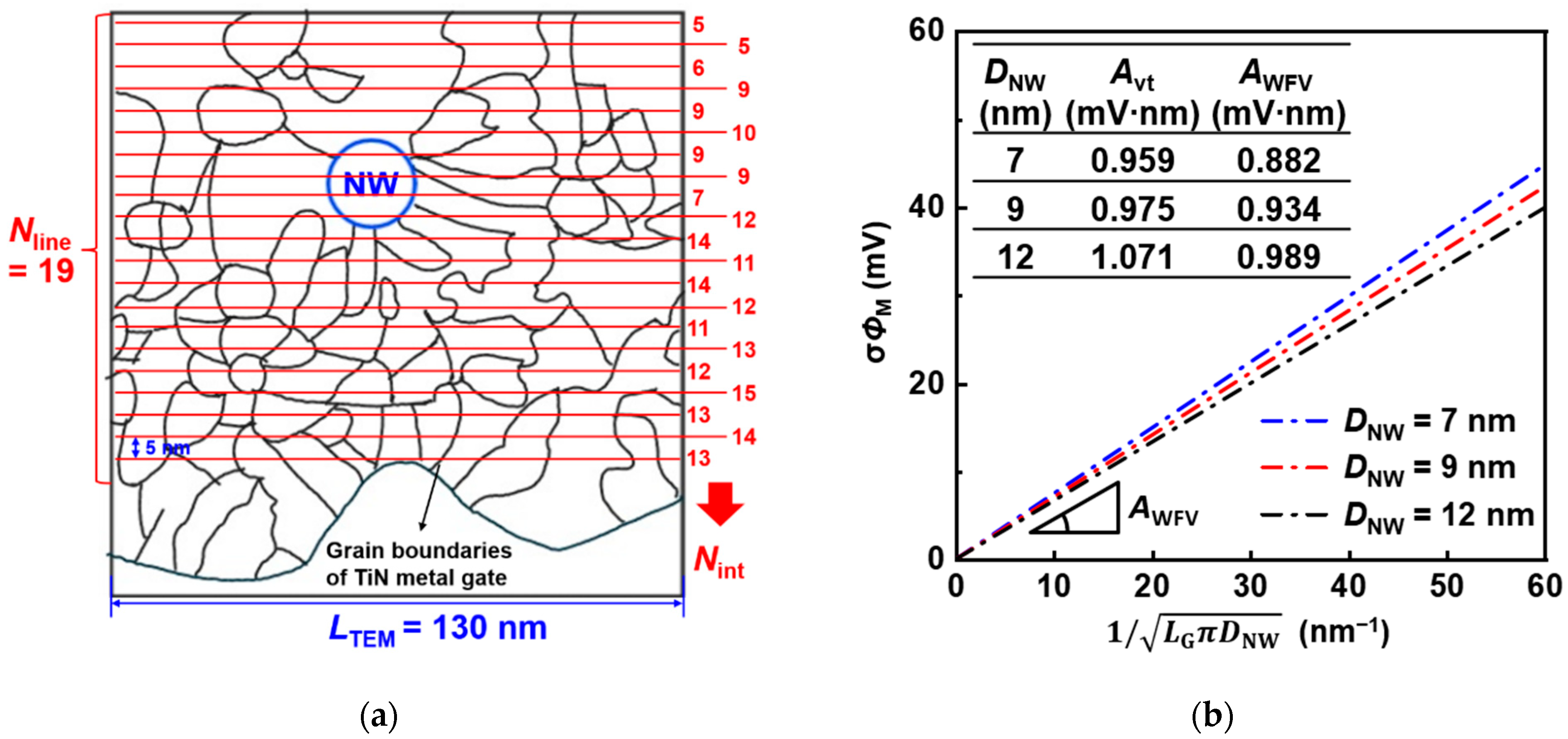
3.2.1. Extraction of Gsize and WFV of SNWFETs

Gsize should be determined from the TEM image of the TiN metal gate of the SNWFET to analyze WFV. Figure 6a shows a schematic of the grain boundaries based on TiN metal gate TEM image [19]. Gsize was measured as the average of values obtained by dividing the length of TiN metal in the TEM image (LTEM) by the number of intersections between grain boundaries and horizontal lines (Nint), as follow [28]:
G size = i = 1 N line L TEM / ( N int ,   i + 1 ) N line ,
where Nline is the number of horizontal lines. The distance between the lines was set to 5 nm, as shown in Figure 6a. Consequently, Gsize measured using Equation (6) was 11.8 nm in SNWFETs. According to previous research, the value of SL is 105 V/nm in SNWFETs [22]. σΦM was calculated by putting obtained Gsize and SL into Equation (3), and Figure 6b shows σΦM as a function of the square root of the channel area. Interestingly, the trend and value of the slope in Figure 6b (AWFV) are very similar to Avt for each DNW. It means WFV induced by MGG is the dominant random variation component of Vth variation in the SNWFETs.

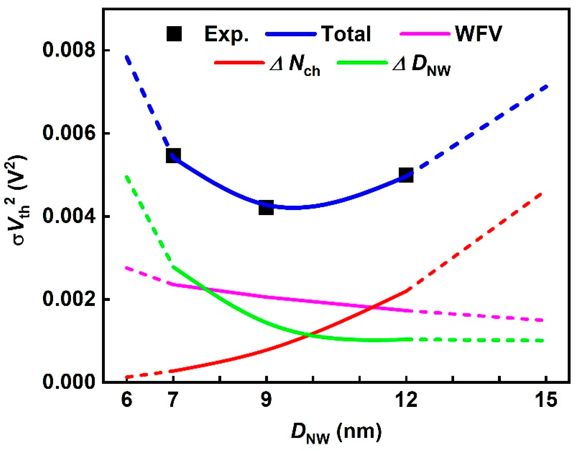
3.2.2. The Contribution of Variation Sources to σVth for Each DNW

Figure 7 shows that Equation (2) accurately fitted the measured σVth with the relative root mean square error of 0.3% where σNch = 1.11 × 1018 cm and σDNW = 0.743 nm. WFV and DNW are slightly correlated because DNW is included in Equation (3), which can affect the modeling accuracy. However, assuming the occurrence of ∆DNW of 0.743 nm, the possible WFV fluctuation is only by 2.4% of total σVth and does not change the DNW tendency of σVth induced by each variation source. The DNW tendency of σVth can be explained by the different contributions of the three variation sources, which are represented using pink (WFV), red (∆Nch), and green (∆DNW) lines in Figure 7. The modeling results are shown considering LG = 15 nm; however, the model was also applied to SNWFET with other LG, and the modeling accuracy and trend of each variation sources are very similar.
Although AMGG decreases when DNW decreases, the contribution of WFV increases owing to the decrease in the channel area. As DNW decreases, SNWFETs become robust to ∆Nch-induced Vth variation. This is because the influence of depletion charge and surface potential is reduced proportional to r nw 2 because of the improvement in gate-controllability, as shown in Equation (4). Conversely, SNWFETs become vulnerable to ∆DNW-induced Vth variation because the sensitivity of Vth to quantum effect is proportional to 1/ r nw 3 , as indicated in Equation (5). Consequently, the contribution of ∆DNW, WFV, and ∆Nch is dominant when at DNW of 7 nm, 9 nm, and 12, respectively.

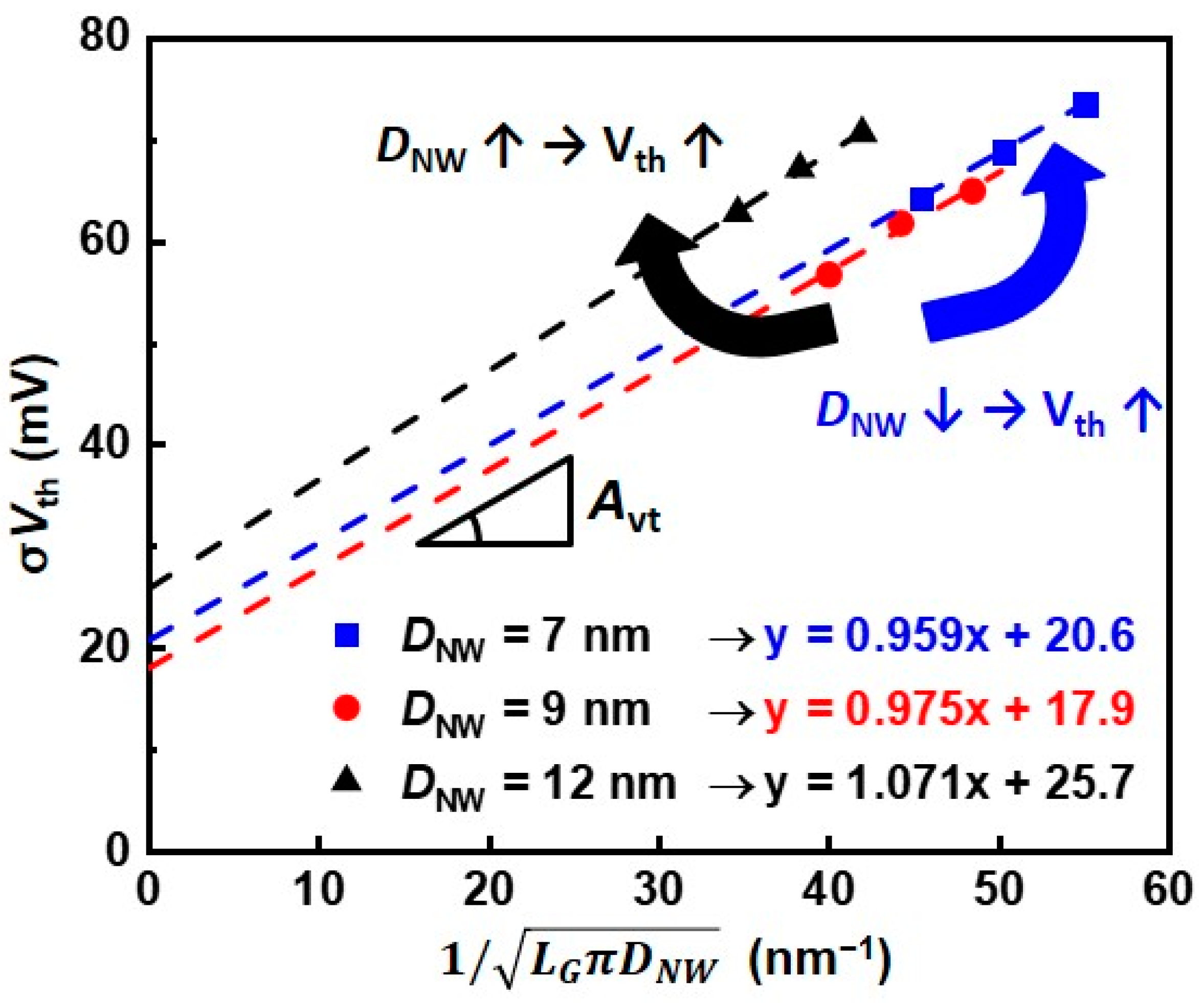
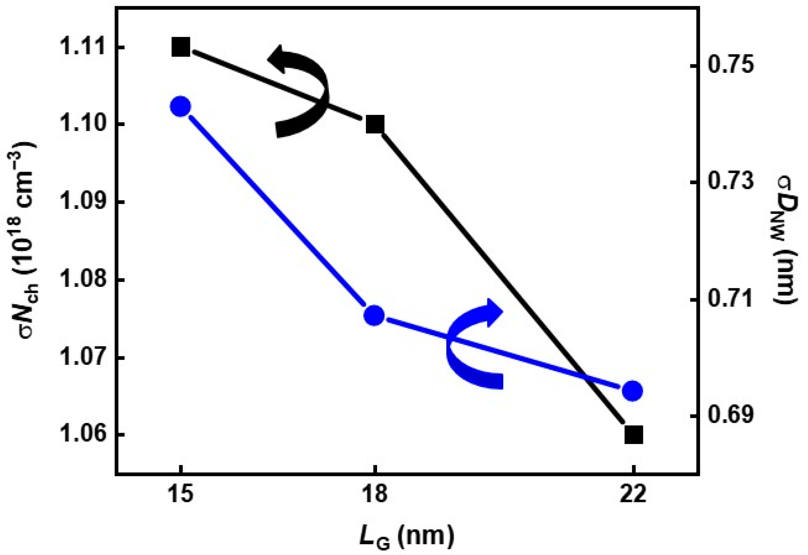
3.2.3. The Tendency of σNch and σDNW as LG Changes

Figure 8 shows both σNch and σDNW increases as LG decreases. This result means that RDF and LER occur because their influence increases as the device dimension decreases. However, the degree of σNch and σDNW increase is small, about 5%, as LG decreases from 22 to 15 nm. In addition, we already verified WFV by MGG is the dominant random variation component of Vth variation in Section 3.2.1. Hence, most ∆Nch and ∆DNW originated from process variation sources, which causes non-zero y-intercept in Figure 3.

4. Conclusions

The contribution of WFV, ∆Nch, and ∆DNW in Vth variation of SNWFET was quantitatively analyzed for each DNW using the novel modeling approach. The sensitivity of WFV against the channel area is similar to that of σVth. As DNW decreases, SNWFETs became robust to ∆Nch but vulnerable to ∆DNW. The dominant variation sources differed for each DNW. Hence, the strategy to improve the variability of SNWFETs should be different for each DNW. Furthermore, with slight modifications, the proposed modeling approach and results are expected to be used in most multigate devices, including FinFET and nanosheet FET.

Author Contributions

Conceptualization, S.L. (Seunghwan Lee) and J.-S.Y.; methodology, S.L. (Seunghwan Lee), J.-S.Y. and H.Y.; formal analysis, S.L. (Seunghwan Lee); investigation, S.L. (Seunghwan Lee), J.L. (Junjong Lee) and J.L. (Jaewan Lim); writing—original draft preparation, S.L. (Seunghwan Lee); writing—review and editing, J.-S.Y., J.J., J.L. (Jaewan Lim) and S.L. (Sanguk Lee); supervision, J.J. and R.-H.B.; project administration, R.-H.B.; funding acquisition, R.-H.B. All authors have read and agreed to the published version of the manuscript.

Funding

This work was supported in part by POSTECH-Samsung Electronics Industry-Academia Cooperative Research Center; National Research Foundation of Korea (NRF) grant funded by the Korea Government (MSIT) (No. NRF-2022R1C1C1004925 and NRF-2020M3F3A2A02082436); and BK21 FOUR Program.

Institutional Review Board Statement

Not applicable.

Informed Consent Statement

Not applicable.

Data Availability Statement

Not applicable.

Acknowledgments

The authors would like to thank the Samsung Electronics Company Ltd., Hwaseong-si 18448, Gyeonggi-do, Korea for device fabrication.

Conflicts of Interest

The authors declare no conflict of interest.

References

  1. Bardon, M.G.; Sherazi, Y.; Schuddinck, P.; Jang, D.; Yakimets, D.; Debacker, P.; Baert, R.; Mertens, H.; Badaroglu, M.; Mocuta, A.; et al. Extreme scaling enabled by 5 tracks cells: Holistic design-device co-optimization for FinFETs and lateral nanowires. In Proceedings of the IEEE International Electron Devices Meeting (IEDM), San Francisco, CA, USA, 3–7 December 2016; pp. 28.2.1–28.2.4. [Google Scholar] [CrossRef]
  2. Li, J.; Li, Y.; Zhou, N.; Xiong, W.; Wang, G.; Zhang, Q.; Du, A.; Gao, J.; Kong, Z.; Lin, H.; et al. Study of Silicon Nitride Inner Spacer Formation in Process of Gate-all-around Nano-Transistors. Nanomaterials 2020, 10, 793. [Google Scholar] [CrossRef] [PubMed]
  3. Cheng, X.; Li, Y.; Zhao, F.; Chen, A.; Liu, H.; Li, C.; Zhang, Q.; Yin, H.; Luo, J.; Wang, W. 4-Levels Vertically Stacked SiGe Channel Nanowires Gate-All-Around Transistor with Novel Channel Releasing and Source and Drain Silicide Process. Nanomaterials 2022, 12, 889. [Google Scholar] [CrossRef] [PubMed]
  4. Pelgrom, M.J.M.; Duinmaijer, A.C.J.; Welbers, A.P.G. Matching properties of MOS transistors. J. Solid-State Circuits 1989, 24, 1433–1439. [Google Scholar] [CrossRef]
  5. Suk, S.D.; Yeoh, Y.Y.; Li, M.; Yeo, K.H.; Kim, S.H.; Kim, D.W.; Park, D.; Lee, W.-S. TSNWFET for SRAM cell application: Performance variation and process dependency. In Proceedings of the IEEE Symposium on VLSI Technology (VLSI), Honolulu, HI, USA, 18–20 June 2008; pp. 38–39. [Google Scholar] [CrossRef]
  6. Seoane, N.; Fernandez, J.G.; Kalna, K.; Comesaña, E.; García-Loureiro, A. Simulations of statistical variability in n-type FinFET, nanowire, and nanosheet FETs. IEEE Electron Device Lett. 2021, 42, 1416–1419. [Google Scholar] [CrossRef]
  7. Espiñeira, G.; Nagy, D.; Indalecio, G.; García-Loureiro, A.J.; Kalna, K.; Seoane, N. Impact of gate edge roughness variability on FinFET and gate-all-around nanowire FET. IEEE Electron Device Lett. 2019, 40, 510–513. [Google Scholar] [CrossRef] [Green Version]
  8. Spinelli, A.S.; Compagnoni, C.M.; Lacaita, A.L. Variability effects in nanowire and macaroni MOSFETs—Part I: Random dopant fluctuations. IEEE Trans. Electron Devices 2020, 67, 1485–1491. [Google Scholar] [CrossRef]
  9. Yoon, J.S.; Rim, T.; Kim, J.; Kim, K.; Baek, C.K.; Jeong, Y.H. Statistical variability study of random dopant fluctuation on gate-all-around inversion-mode silicon nanowire field-effect transistors. Appl. Phys. Lett. 2015, 106, 103507. [Google Scholar] [CrossRef] [Green Version]
  10. Bansal, A.K.; Gupta, C.; Gupta, A.; Singh, R.; Hook, T.B.; Dixit, A. 3-D LER and RDF matching performance of nanowire FETs in inversion, accumulation, and junctionless modes. IEEE Trans. Electron Devices 2018, 65, 1246–1252. [Google Scholar] [CrossRef]
  11. Li, Y.; Chang, H.T.; Lai, C.N.; Chao, P.J.; Chen, C.Y. Process variation effect, metal-gate work-function fluctuation and random dopant fluctuation of 10-nm gate-all-around silicon nanowire MOSFET devices. In Proceedings of the IEEE International Electron Devices Meeting (IEDM), Washington, DC, USA, 7–9 December 2015; pp. 34.4.1–34.4.4. [Google Scholar]
  12. Paul, A.; Bryant, A.; Hook, T.B.; Yeh, C.C.; Kamineni, V.; Johnson, J.B.; Tripathi, N.; Yamashita, T.; Tsutsui, G.; Basker, V.; et al. Comprehensive study of effective current variability and MOSFET parameter correlations in 14nm multi-fin SOI FINFETs. In Proceedings of the IEEE International Electron Devices Meeting (IEDM), Washington, DC, USA, 9–11 December 2013; pp. 13.5.1–13.5.4. [Google Scholar] [CrossRef]
  13. Sugii, N.; Tsuchiya, R.; Ishigaki, T.; Morita, Y.; Yoshimoto, H.; Torii, K.; Kimura, S.I. Comprehensive study on Vth variability in silicon on thin BOX (SOTB) CMOS with small random-dopant fluctuation: Finding a way to further reduce variation. In Proceedings of the IEEE International Electron Devices Meeting (IEDM), San Francisco, CA, USA, 15–17 December 2008; pp. 1–4. [Google Scholar] [CrossRef]
  14. Hook, T.B.; Vinet, M.; Murphy, R.; Ponoth, S.; Grenouillet, L. Transistor matching and silicon thickness variation in ETSOI technology. In Proceedings of the IEEE International Electron Devices Meeting (IEDM), Washington, DC, USA, 5–7 December 2011; pp. 5.7.1–5.7.4. [Google Scholar] [CrossRef]
  15. Wang, R.; Zhuge, J.; Huang, R.; Yu, T.; Zou, J.; Kim, D.W.; Park, D.; Wang, Y. Investigation on variability in metal-gate Si nanowire MOSFETs: Analysis of variation sources and experimental characterization. IEEE Trans. Electron Devices 2011, 58, 2317–2325. [Google Scholar] [CrossRef]
  16. Endo, K.; O’uchi, S.I.; Ishikawa, Y.; Liu, Y.; Matsukawa, T.; Sakamoto, K.; Tsukada, J.; Yamauchi, H.; Masahara, M. Variability Analysis of TiN Metal-Gate FinFETs. IEEE Electron Device Lett. 2010, 31, 546–548. [Google Scholar] [CrossRef]
  17. Bhoir, M.S.; Chiarella, T.; Ragnarsson, L.Å.; Mitard, J.; Horiguchi, N.; Mohapatra, N.R. Variability sources in nanoscale bulk FinFETs and TiTaN-a promising low variability WFM for 7/5 nm CMOS nodes. In Proceedings of the International Electron Devices Meeting (IEDM), San Francisco, CA, USA, 7–11 December 2019; pp. 36.2.1–36.2.4. [Google Scholar]
  18. Lee, S.; Yoon, J.S.; Jeong, J.; Lee, J.; Baek, R.H. Observation of mobility and velocity behaviors in ultra-scaled LG = 15 nm silicon nanowire field-effect transistors with different channel diameters. Solid-State Electron. 2020, 164, 107740. [Google Scholar] [CrossRef]
  19. Li, M.; Yeo, K.H.; Suk, S.D.; Yeoh, Y.Y.; Kim, D.W.; Chung, T.Y.; Oh, K.S.; Lee, W.S. Sub-10 nm gate-all-around CMOS nanowire transistors on bulk Si substrate. In Proceedings of the IEEE Symposium on VLSI Technology (VLSI), Kyoto, Japan, 15–17 June 2009; pp. 94–95. [Google Scholar]
  20. Kim, D.W.; Yeo, K.; Suk, S.D.; Li, M.; Yeoh, Y.Y.; Sohn, D.K.; Chung, C. Fabrication and electrical characteristics of self-aligned (SA) gate-all-around (GAA) Si nanowire MOSFETs (SNWFET). In Proceedings of the IEEE International Conference on Integrated Circuit Design and Technology, Grenoble, France, 2–4 June 2010; pp. 63–66. [Google Scholar] [CrossRef]
  21. Akbari-Saatlu, M.; Procek, M.; Mattsson, C.; Thungström, G.; Nilsson, H.-E.; Xiong, W.; Xu, B.; Li, Y.; Radamson, H.H. Silicon Nanowires for Gas Sensing: A Review. Nanomaterials 2020, 10, 2215. [Google Scholar] [CrossRef] [PubMed]
  22. Nam, H.; Lee, Y.; Park, J.D.; Shin, C. Study of Work-Function Variation in High-k Metal-Gate Gate-All-Around Nanowire MOSFET. IEEE Trans. Electron Devices 2016, 63, 3338–3341. [Google Scholar] [CrossRef]
  23. Yoon, J.S.; Lee, S.; Yun, H.; Baek, R.H. Digital/Analog performance optimization of vertical nanowire FETs using machine learning. IEEE Access 2021, 9, 29071–29077. [Google Scholar] [CrossRef]
  24. Kuhn, K.J.; Giles, M.D.; Becher, D.; Kolar, P.; Kornfeld, A.; Kotlyar, R.; Ma, S.T.; Maheshwari, A.; Mudanai, S. Process technology variation. IEEE Trans. Electron Devices 2011, 58, 2197–2208. [Google Scholar] [CrossRef]
  25. Trevisoli, R.D.; Doria, R.T.; Pavanello, M.A. Analytical model for the threshold voltage in junctionless nanowire transistors of different geometries. ECS Trans. 2011, 39, 147–154. [Google Scholar] [CrossRef]
  26. Trevisoli, R.D.; Doria, R.T.; de Souza, M.; Pavanello, M.A. Threshold voltage in junctionless nanowire transistors. Semicond. Sci. Technol. 2011, 26, 105009. [Google Scholar] [CrossRef]
  27. Matsukawa, T.; Liu, Y.; O’uchi, S.I.; Endo, K.; Tsukada, J.; Yamauchi, H.; Ishikawa, Y.; Ota, H.; Migita, S.; Morita, Y.; et al. Comprehensive analysis of Ion variation in metal gate FinFETs for 20 nm and beyond. In Proceedings of the IEEE International Electron Devices Meeting (IEDM), Washington, DC, USA, 5–7 December 2011; pp. 23.5.1–23.5.4. [Google Scholar] [CrossRef]
  28. Rawat, A.; Sharan, N.; Jang, D.; Chiarella, T.; Bufler, F.M.; Catthoor, F.; Parvais, B.; Ganguly, U. Experimental validation of process-induced variability aware SPICE simulation platform for sub-20 nm FinFET technologies. IEEE Trans. Electron Devices 2021, 68, 976–980. [Google Scholar] [CrossRef]
Figure 1. Schematic of the silicon nanowire field-effect transistor (SNWFET) and possible Vth variation sources.
Nanomaterials 12 01721 g001
Figure 2. (a) Vth fluctuation in IDVG of silicon nanowire field-effect transistors (SNWFETs) with LG = 15 nm and DNW = 7 nm. Vth is directly extracted using the constant current method at ID = 10−7πDNW/LG. (b) Quantile plot of Vth of the SNWFET with LG = 15 nm.
Nanomaterials 12 01721 g002
Figure 3. Pelgrom plot for Vth variation of the silicon nanowire field−effect transistors (SNWFETs).
Nanomaterials 12 01721 g003
Figure 4. Flowchart of the proposed σVth modeling process.
Nanomaterials 12 01721 g004
Figure 5. (a) Measured (black dots) and modeled (blue line) values of Vth as a function of DNW. (b) Extracted Nch as a function of LG.
Nanomaterials 12 01721 g005
Figure 6. (a) Grain boundaries estimated from [19] and red horizontal lines to estimate Gsize of TiN metal gate of SNWFETs. (b) Pelgrom’s plot only considering work function variation (WFV) by metal gate granularity (MGG).
Nanomaterials 12 01721 g006
Figure 7. Model fitting results (blue line) considering WFV (pink line), ∆Nch (red line), and ∆DNW (green line) for the measured value of squared σVth (black dots). The model fits were extrapolated for DNW of 6 and 15 nm (dashed line).
Nanomaterials 12 01721 g007
Figure 8. Extracted σNch (black line) and σDNW (blue line) as function of LG.
Nanomaterials 12 01721 g008
Publisher’s Note: MDPI stays neutral with regard to jurisdictional claims in published maps and institutional affiliations.

