
Enhancement of Luminous Intensity Emission from Incoherent LED Light Sources within the Detection Angle of 10° Using Metalenses


Abstract
:1. Introduction
2. Results and Discussion
2.1. Light Source Design for Simulation
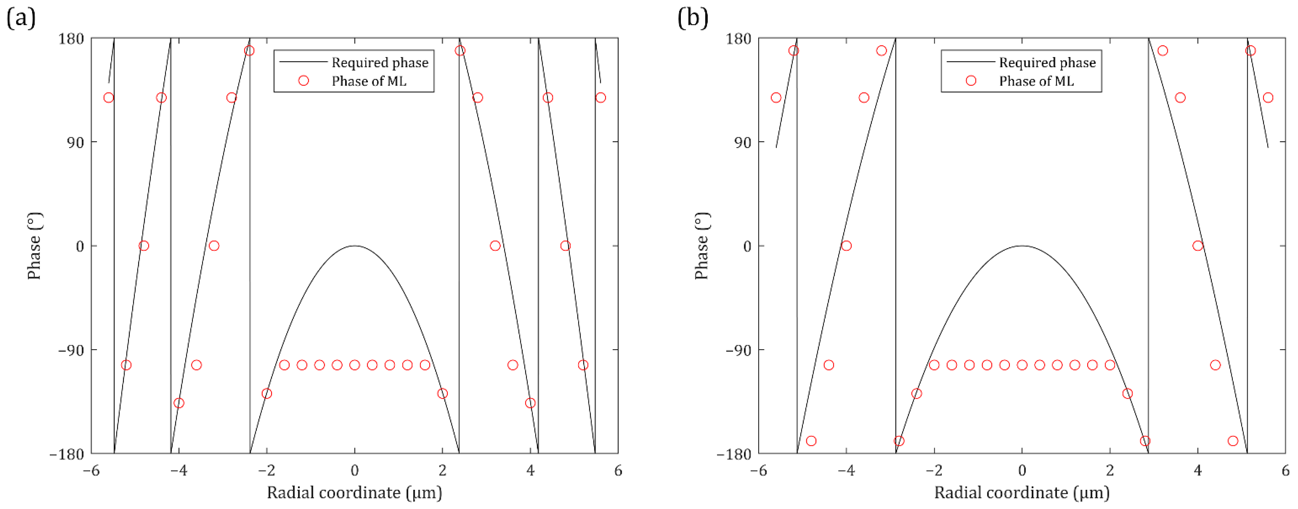
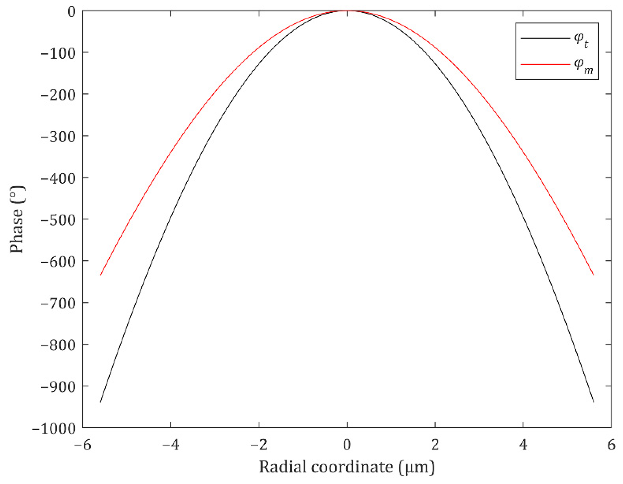
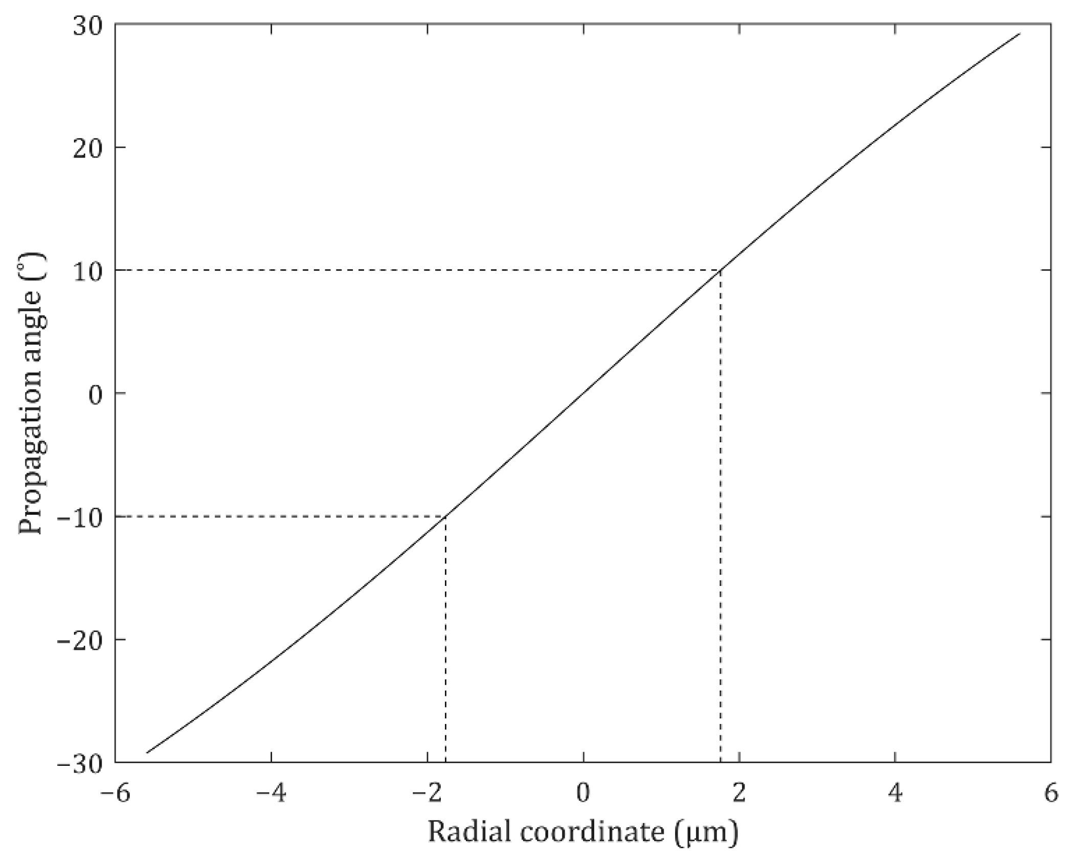
2.2. Phase Profile of Metalens
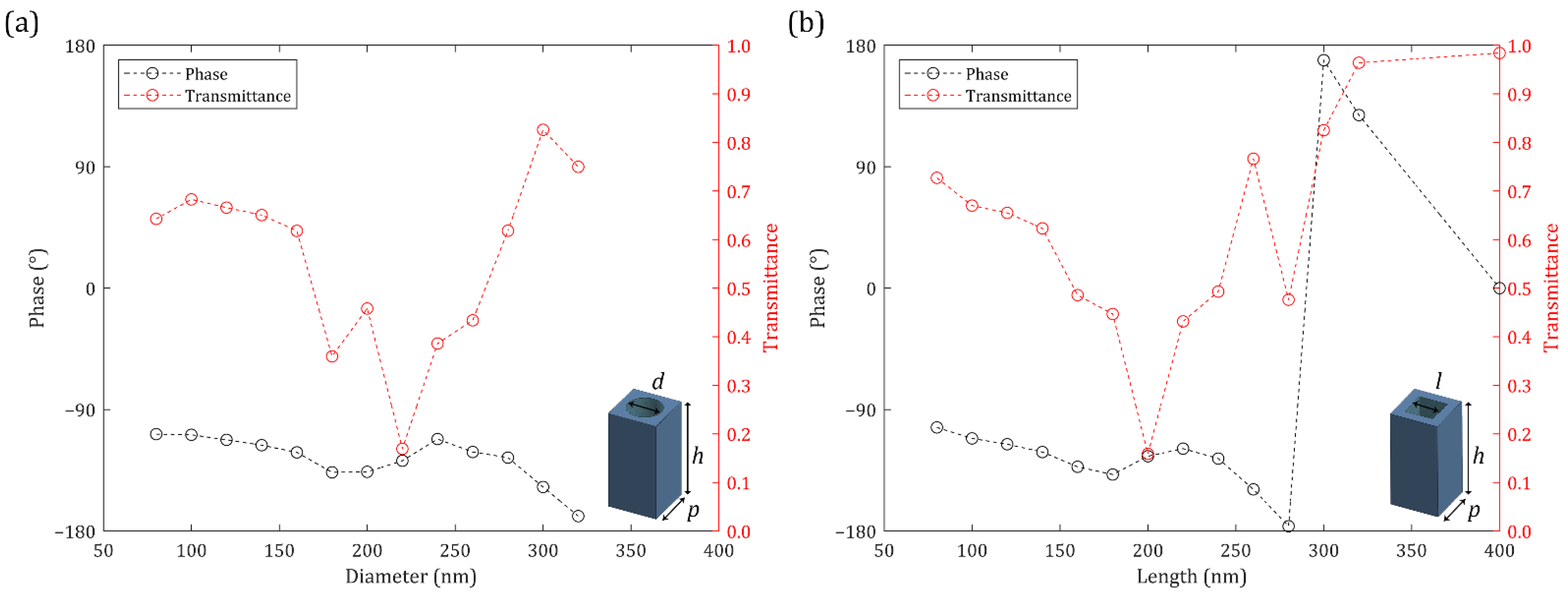
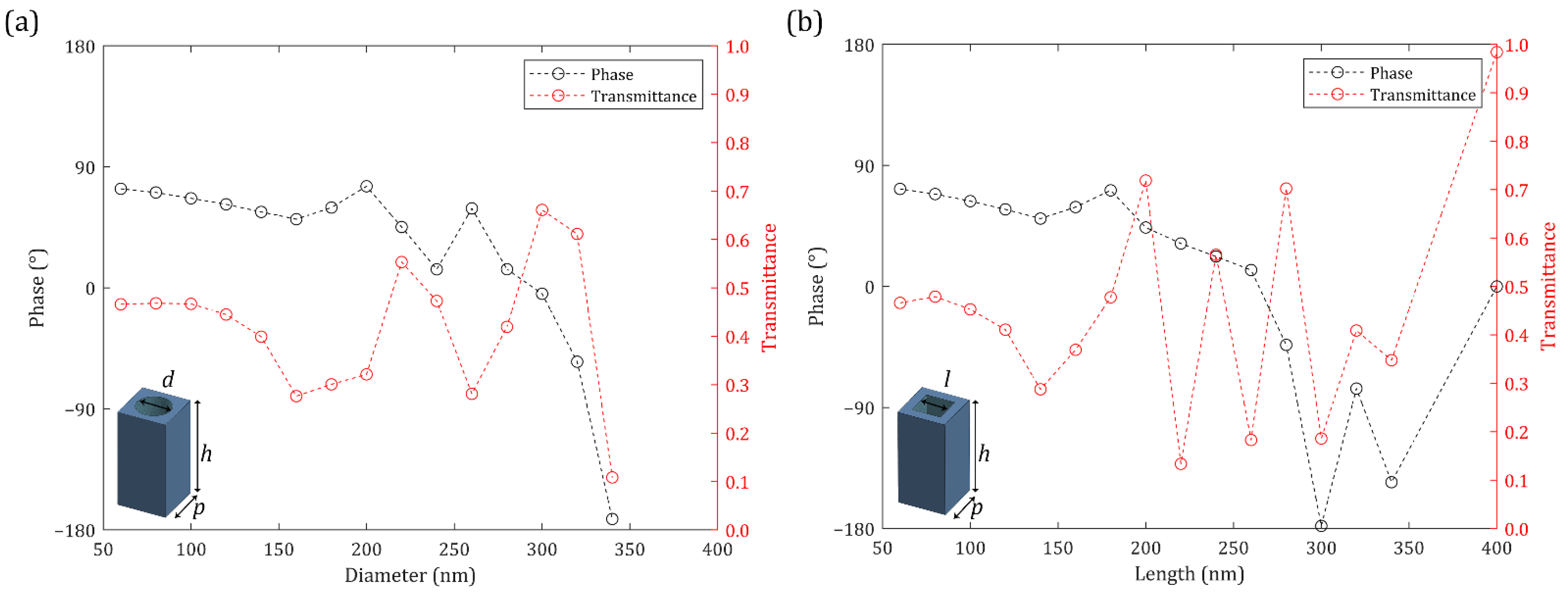
2.3. Nanohole Meta-Atom
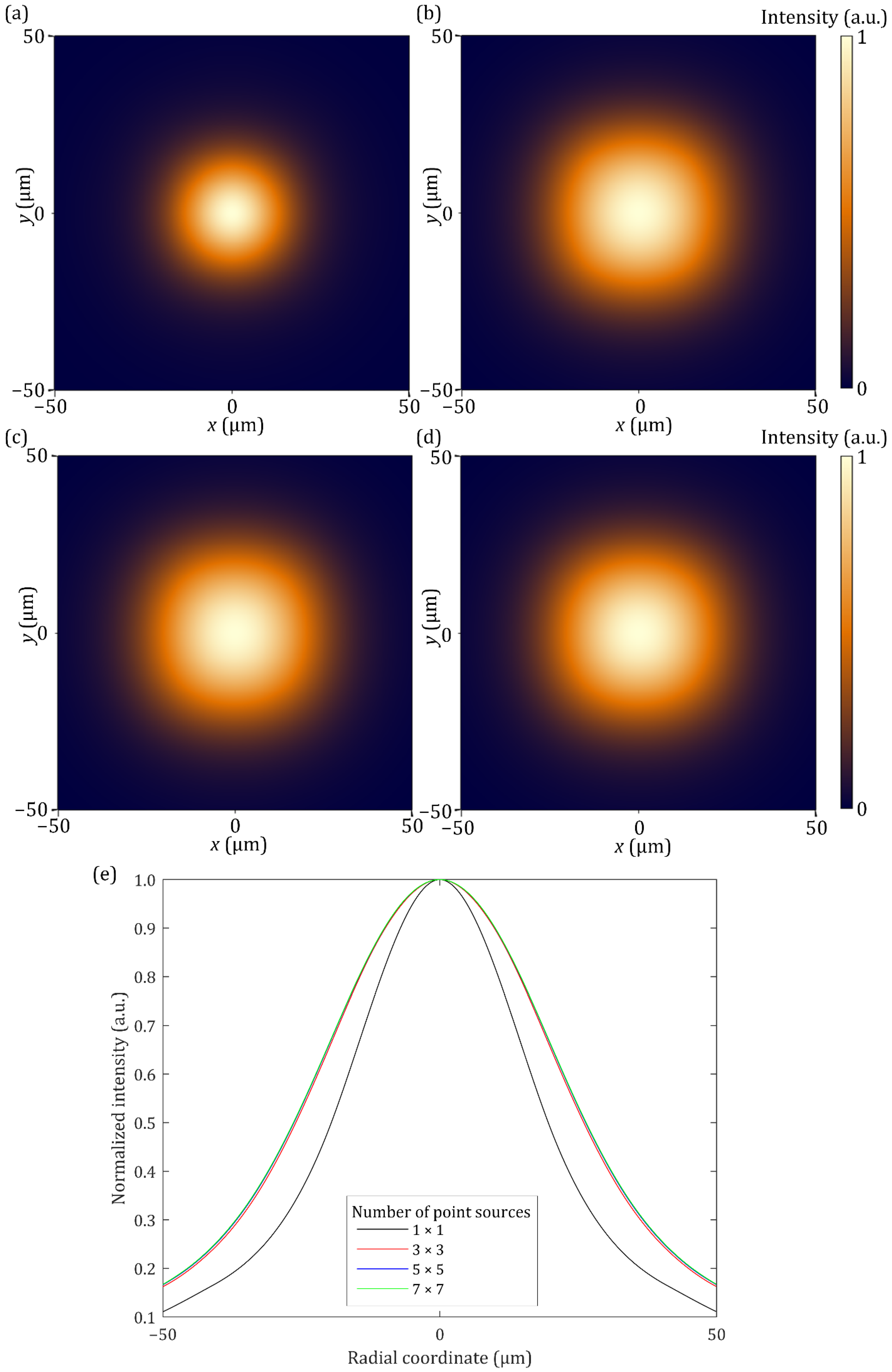
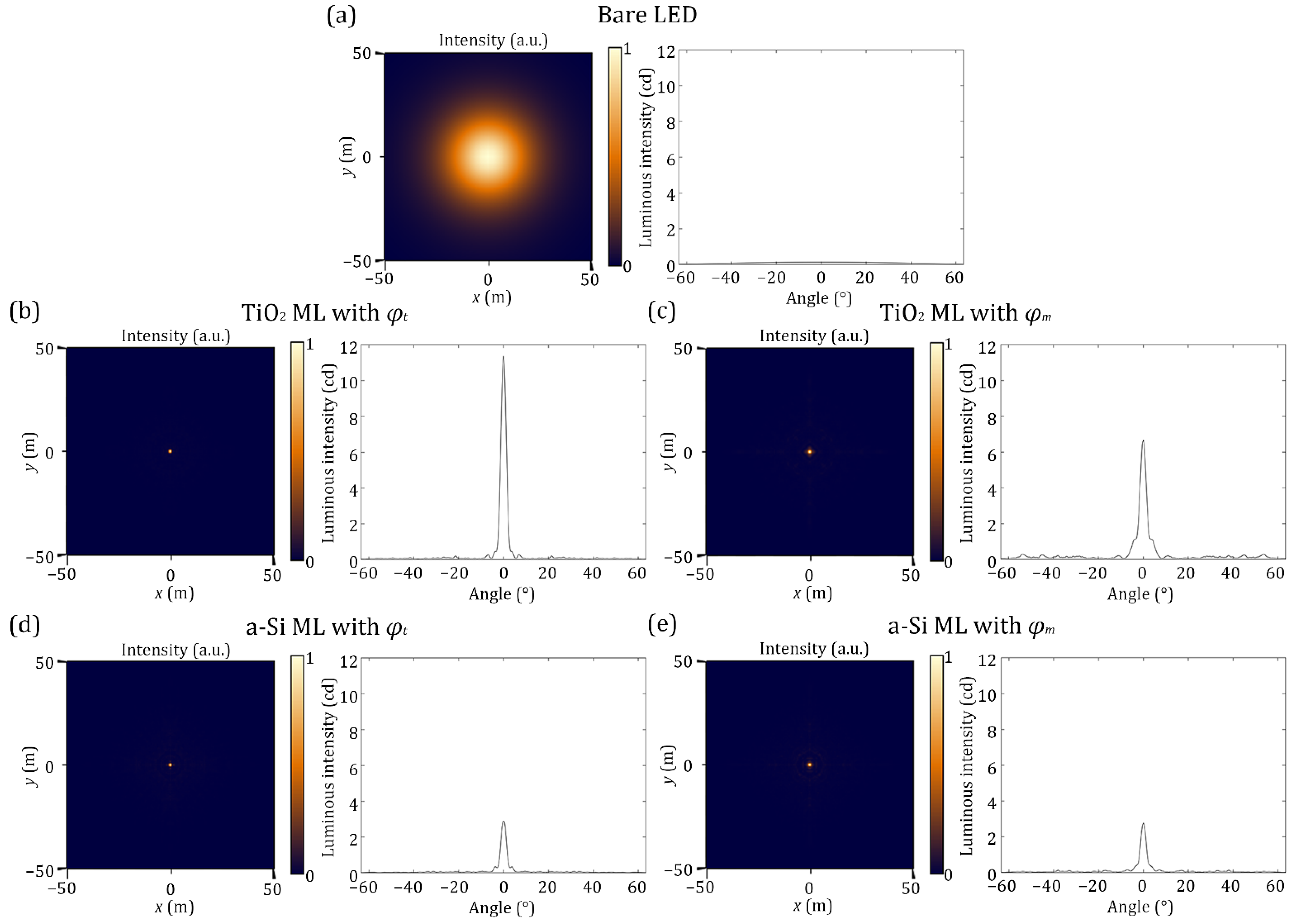
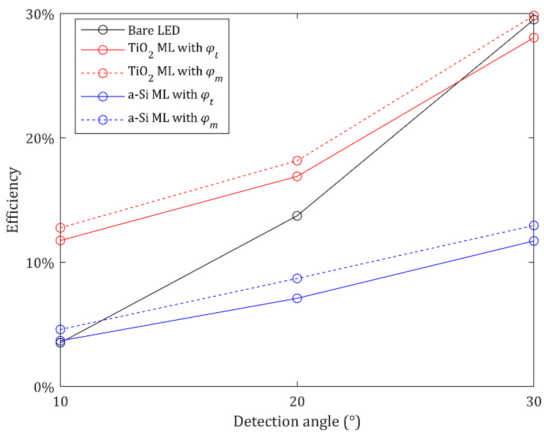
2.4. Far Field Propagation Simulation
3. Conclusions
4. Methods
Supplementary Materials
Author Contributions
Funding
Institutional Review Board Statement
Informed Consent Statement
Data Availability Statement
Conflicts of Interest
References
- Yu, N.; Capasso, F. Flat optics with designer metasurfaces. Nat. Mater. 2014, 13, 139–150. [Google Scholar] [CrossRef] [PubMed]
- Dolling, G.; Enkrich, C.; Wegener, M.; Soukoulis, C.M.; Linden, S. Simultaneous negative phase and group velocity of light in a metamaterial. Science 2006, 312, 892–894. [Google Scholar] [CrossRef] [PubMed] [Green Version]
- Kristensen, A.; Yang, J.K.W.; Bozhevolnyi, S.I.; Link, S.; Nordlander, P.; Halas, N.J.; Mortensen, N.A. Plasmonic colour generation. Nat. Rev. Mater. 2016, 2, 16088. [Google Scholar] [CrossRef]
- Lee, T.; Jang, J.; Jeong, H.; Rho, J. Plasmonic- and dielectric-based structural coloring: From fundamentals to practical applications. Nano Converg. 2018, 5, 1. [Google Scholar] [CrossRef] [PubMed] [Green Version]
- Badloe, T.; Mun, J.; Rho, J. Metasurfaces-Based Absorption and Reflection Control: Perfect Absorbers and Reflectors. J. Nanomater. 2017, 2017, 2361042. [Google Scholar] [CrossRef] [Green Version]
- Hao, J.; Yuan, Y.; Ran, L.; Jiang, T.; Kong, J.A.; Chan, C.T.; Zhou, L. Manipulating electromagnetic wave polarizations by anisotropic metamaterials. Phys. Rev. Lett. 2007, 99, 063908. [Google Scholar] [CrossRef] [Green Version]
- Yoon, G.; Lee, D.; Nam, K.T.; Rho, J. Geometric metasurface enabling polarization independent beam splitting. Sci. Rep. 2018, 8, 9468. [Google Scholar] [CrossRef] [PubMed] [Green Version]
- Khorasaninejad, M.; Chen, W.T.; Devlin, R.C.; Oh, J.; Zhu, A.Y.; Capasso, F. Metalenses at visible wavelengths: Diffraction-limited focusing and subwavelength resolution imaging. Science 2016, 352, 1190–1194. [Google Scholar] [CrossRef] [Green Version]
- Lee, D.; Gwak, J.; Badloe, T.; Palomba, S.; Rho, J. Metasurfaces-based imaging and applications: From miniaturized optical components to functional imaging platforms. Nanoscale Adv. 2020, 2, 605–625. [Google Scholar] [CrossRef] [Green Version]
- Moon, S.W.; Kim, Y.; Yoon, G.; Rho, J. Recent Progress on Ultrathin Metalenses for Flat Optics. iScience 2020, 23, 101877. [Google Scholar] [CrossRef]
- Lee, T.; Lee, C.; Oh, D.K.; Badloe, T.; Ok, J.G.; Rho, J. Scalable and high-throughput top-down manufacturing of optical metasurfaces. Sensors 2020, 20, 4108. [Google Scholar] [CrossRef] [PubMed]
- Kim, M.; Rho, J. Metamaterials and imaging. Nano Converg. 2015, 2, 22. [Google Scholar] [CrossRef] [PubMed] [Green Version]
- Yoon, G.; Tanaka, T.; Zentgraf, T.; Rho, J. Recent progress on metasurfaces: Applications and fabrication. J. Phys. D Appl. Phys. 2021, 54, 383002. [Google Scholar] [CrossRef]
- Jung, C.; Kim, G.; Jeong, M.; Jang, J.; Dong, Z.; Badloe, T.; Yang, J.K.W.; Rho, J. Metasurface-Driven Optically Variable Devices. Chem. Rev. 2021, 121, 13013–13050. [Google Scholar] [CrossRef]
- Ansari, M.A.; Kim, I.; Lee, D.; Waseem, M.H.; Zubair, M.; Mahmood, N.; Badloe, T.; Yerci, S.; Tauqeer, T.; Mehmood, M.Q.; et al. A Spin-Encoded All-Dielectric Metahologram for Visible Light. Laser Photonics Rev. 2019, 13, 1900065. [Google Scholar] [CrossRef]
- Naveed, M.A.; Ansari, M.A.; Kim, I.; Badloe, T.; Kim, J.; Oh, D.K.; Riaz, K.; Tauqeer, T.; Younis, U.; Saleem, M.; et al. Optical spin-symmetry breaking for high-efficiency directional helicity-multiplexed metaholograms. Microsyst. Nanoeng. 2021, 7, 5. [Google Scholar] [CrossRef]
- Yoon, G.; Lee, D.; Nam, K.T.; Rho, J. Pragmatic Metasurface Hologram at Visible Wavelength: The Balance between Diffraction Efficiency and Fabrication Compatibility. ACS Photonics 2018, 5, 1643–1647. [Google Scholar] [CrossRef]
- Kim, I.; Ansari, M.A.; Mehmood, M.Q.; Kim, W.S.; Jang, J.; Zubair, M.; Kim, Y.K.; Rho, J. Stimuli-Responsive Dynamic Metaholographic Displays with Designer Liquid Crystal Modulators. Adv. Mater. 2020, 32, 2004664. [Google Scholar] [CrossRef]
- Ansari, M.A.; Kim, I.; Rukhlenko, I.D.; Zubair, M.; Yerci, S.; Tauqeer, T.; Mehmood, M.Q.; Rho, J. Engineering spin and antiferromagnetic resonances to realize an efficient direction-multiplexed visible meta-hologram. Nanoscale Horiz. 2019. [Google Scholar] [CrossRef]
- Li, X.; Ren, H.; Chen, X.; Liu, J.; Li, Q.; Li, C.; Xue, G.; Jia, J.; Cao, L.; Sahu, A.; et al. Athermally photoreduced graphene oxides for three-dimensional holographic images. Nat. Commun. 2015, 6, 6984. [Google Scholar] [CrossRef] [Green Version]
- Yoon, G.; Lee, D.; Nam, K.T.; Rho, J. “Crypto-Display” in Dual-Mode Metasurfaces by Simultaneous Control of Phase and Spectral Responses. ACS Nano 2018, 12, 6421–6428. [Google Scholar] [CrossRef]
- Lee, G.-Y.; Yoon, G.; Lee, S.-Y.; Yun, H.; Cho, J.; Lee, K.; Kim, H.; Rho, J.; Lee, B. Complete amplitude and phase control of light using broadband holographic metasurfaces. Nanoscale 2018, 10, 4237–4245. [Google Scholar] [CrossRef] [Green Version]
- Zheng, G.; Mühlenbernd, H.; Kenney, M.; Li, G.; Zentgraf, T.; Zhang, S. Metasurface holograms reaching 80% efficiency. Nat. Nanotechnol. 2015, 10, 308. [Google Scholar] [CrossRef]
- Zhou, Y.; Kravchenko, I.I.; Wang, H.; Zheng, H.; Gu, G.; Valentine, J. Multifunctional metaoptics based on bilayer metasurfaces. Light Sci. Appl. 2019, 8, 80. [Google Scholar] [CrossRef] [Green Version]
- Kim, I.; Jang, J.; Kim, G.; Lee, J.; Badloe, T.; Mun, J.; Rho, J. Pixelated bifunctional metasurface-driven dynamic vectorial holographic color prints for photonic security platform. Nat. Commun. 2021, 12, 3614. [Google Scholar] [CrossRef] [PubMed]
- Ren, H.; Fang, X.; Jang, J.; Bürger, J.; Rho, J.; Maier, S.A. Complex-amplitude metasurface-based orbital angular momentum holography in momentum space. Nat. Nanotechnol. 2020, 15, 948–955. [Google Scholar] [CrossRef] [PubMed]
- Kim, I.; Yoon, G.; Jang, J.; Genevet, P.; Nam, K.T.; Rho, J. Outfitting Next Generation Displays with Optical Metasurfaces. ACS Photonics 2018, 5, 3876–3895. [Google Scholar] [CrossRef]
- Jang, J.; Jeong, H.; Hu, G.; Qiu, C.-W.; Nam, K.T.; Rho, J. Kerker-Conditioned Dynamic Cryptographic Nanoprints. Adv. Opt. Mater. 2019, 7, 1801070. [Google Scholar] [CrossRef] [Green Version]
- Tseng, M.L.; Yang, J.; Semmlinger, M.; Zhang, C.; Nordlander, P.; Halas, N.J. Two-Dimensional Active Tuning of an Aluminum Plasmonic Array for Full-Spectrum Response. Nano Lett. 2017, 17, 6034–6039. [Google Scholar] [CrossRef]
- Yang, B.; Liu, W.; Li, Z.; Cheng, H.; Choi, D.-Y.; Chen, S.; Tian, J. Ultrahighly Saturated Structural Colors Enhanced by Multipolar-Modulated Metasurfaces. Nano Lett. 2019, 19, 4221–4228. [Google Scholar] [CrossRef]
- Jang, J.; Badloe, T.; Yang, Y.; Lee, T.; Mun, J.; Rho, J. Spectral modulation through the hybridization of Mie-scatterers and quasi-guided mode resonances: Realizing full and gradients of structural color. ACS Nano 2020, 14, 15317–15326. [Google Scholar] [CrossRef]
- Wu, P.C.; Pala, R.A.; Kafaie Shirmanesh, G.; Cheng, W.H.; Sokhoyan, R.; Grajower, M.; Alam, M.Z.; Lee, D.; Atwater, H.A. Dynamic beam steering with all-dielectric electro-optic III–V multiple-quantum-well metasurfaces. Nat. Commun. 2019, 10, 3654. [Google Scholar] [CrossRef]
- Holsteen, A.L.; Cihan, A.F.; Brongersma, M.L. Temporal color mixing and dynamic beam shaping with silicon metasurfaces. Science 2019, 365, 257–260. [Google Scholar] [CrossRef]
- Wang, L.; Ng, R.J.H.; Safari Dinachali, S.; Jalali, M.; Yu, Y.; Yang, J.K.W. Large Area Plasmonic Color Palettes with Expanded Gamut Using Colloidal Self-Assembly. ACS Photonics 2016, 3, 627–633. [Google Scholar] [CrossRef]
- Li, Z.; Dai, Q.; Mehmood, M.Q.; Hu, G.; Yanchuk, B.L.; Tao, J.; Hao, C.; Kim, I.; Jeong, H.; Zheng, G.; et al. Full-space Cloud of Random Points with a Scrambling Metasurface. Light Sci. Appl. 2018, 7, 63. [Google Scholar] [CrossRef] [PubMed]
- Xie, Y.Y.; Ni, P.N.; Wang, Q.H.; Kan, Q.; Briere, G.; Chen, P.P.; Zhao, Z.Z.; Delga, A.; Ren, H.R.; Da Chen, H.; et al. Metasurface-integrated vertical cavity surface-emitting lasers for programmable directional lasing emissions. Nat. Nanotechnol. 2020, 15, 125–130. [Google Scholar] [CrossRef] [PubMed] [Green Version]
- Kim, I.; Martins, R.J.; Jang, J.; Badloe, T.; Khadir, S.; Jung, H.Y.; Kim, H.; Kim, J.; Genevet, P.; Rho, J. Nanophotonics for light detection and ranging technology. Nat. Nanotechnol. 2021, 16, 508–524. [Google Scholar] [CrossRef] [PubMed]
- Lee, C.W.; Choi, H.J.; Jeong, H. Tunable metasurfaces for visible and SWIR applications. Nano Converg. 2020, 7, 18. [Google Scholar] [CrossRef] [Green Version]
- Yao, Y.; Shankar, R.; Kats, M.A.; Song, Y.; Kong, J.; Loncar, M.; Capasso, F. Electrically tunable metasurface perfect absorbers for ultrathin mid-infrared optical modulators. Nano Lett. 2014, 14, 6526–6532. [Google Scholar] [CrossRef]
- Yoon, G.; So, S.; Kim, M.; Mun, J.; Ma, R.; Rho, J. Electrically tunable metasurface perfect absorber for infrared frequencies. Nano Converg. 2017, 4, 36. [Google Scholar] [CrossRef]
- Zhao, Y.; Askarpour, A.N.; Sun, L.; Shi, J.; Li, X.; Alu, A. Chirality detection of enantiomers using twisted optical metamaterials. Nat. Commun. 2017, 8, 14180. [Google Scholar] [CrossRef]
- Jang, J.; Kang, K.; Raeis-Hosseini, N.; Ismukhanova, A.; Jeong, H.; Jung, C.; Kim, B.; Lee, J.Y.; Park, I.; Rho, J. Self-Powered Humidity Sensor Using Chitosan-Based Plasmonic Metal–Hydrogel–Metal Filters. Adv. Opt. Mater. 2020, 8, 1901932. [Google Scholar] [CrossRef]
- Yang, Y.; Lee, T.; Kim, M.; Jung, C.; Badloe, T.; Lee, D.; Lee, S.; Lee, H.J.; Rho, J. Dynamic Optical Spin Hall Effect in Chitosan-Coated All-Dielectric Metamaterials for a Biosensing Platform. IEEE J. Sel. Top. Quantum Electron. 2021, 27, 7300608. [Google Scholar] [CrossRef]
- Seo, M.H.; Kang, K.; Yoo, J.Y.; Park, J.; Lee, J.S.; Cho, I.; Kim, B.J.; Jeong, Y.; Lee, J.Y.; Kim, B.; et al. Chemo-Mechanically Operating Palladium-Polymer Nanograting Film for a Self-Powered H2 Gas Sensor. ACS Nano 2020, 14, 16813–16822. [Google Scholar] [CrossRef] [PubMed]
- Kim, I.; Kim, W.S.; Kim, K.; Ansari, M.A.; Mehmood, M.Q.; Badloe, T.; Kim, Y.; Gwak, J.; Lee, H.; Kim, Y.K.; et al. Holographic metasurface gas sensors for instantaneous visual alarms. Sci. Adv. 2021, 7, eabe9943. [Google Scholar] [CrossRef] [PubMed]
- Kim, J.; Rana, A.S.; Kim, Y.; Kim, I.; Badloe, T.; Zubair, M.; Mehmood, M.Q.; Rho, J. Chiroptical Metasurfaces: Principles, Classification, and Applications. Sensors 2021, 21, 4381. [Google Scholar] [CrossRef] [PubMed]
- Park, Y.M.; Lim, S.Y.; Jeong, S.W.; Song, Y.; Bae, N.H.; Hong, S.B.; Choi, B.G.; Lee, S.J.; Lee, K.G. Flexible nanopillar-based electrochemical sensors for genetic detection of foodborne pathogens. Nano Converg. 2018, 5, 15. [Google Scholar] [CrossRef]
- Chen, W.T.; Zhu, A.Y.; Sanjeev, V.; Khorasaninejad, M.; Shi, Z.; Lee, E.; Capasso, F. A broadband achromatic metalens for focusing and imaging in the visible. Nat. Nanotechnol. 2018, 13, 220–226. [Google Scholar] [CrossRef] [Green Version]
- Wang, S.; Wu, P.C.; Su, V.C.; Lai, Y.C.; Chen, M.K.; Kuo, H.Y.; Chen, B.H.; Chen, Y.H.; Huang, T.T.; Wang, J.H.; et al. A broadband achromatic metalens in the visible. Nat. Nanotechnol. 2018, 13, 227–232. [Google Scholar] [CrossRef]
- Chen, W.T.; Zhu, A.Y.; Sisler, J.; Bharwani, Z.; Capasso, F. A broadband achromatic polarization-insensitive metalens consisting of anisotropic nanostructures. Nat. Commun. 2019, 10, 355. [Google Scholar] [CrossRef] [Green Version]
- Khorasaninejad, M.; Zhu, A.Y.; Roques-Carmes, C.; Chen, W.T.; Oh, J.; Mishra, I.; Devlin, R.C.; Capasso, F. Polarization-Insensitive Metalenses at Visible Wavelengths. Nano Lett. 2016, 16, 7229–7234. [Google Scholar] [CrossRef]
- Shalaginov, M.Y.; An, S.; Yang, F.; Su, P.; Lyzwa, D.; Agarwal, A.M.; Zhang, H.; Hu, J.; Gu, T. Single-Element Diffraction-Limited Fisheye Metalens. Nano Lett. 2020, 20, 7429–7437. [Google Scholar] [CrossRef]
- Groever, B.; Chen, W.T.; Capasso, F. Meta-lens doublet in the visible region. Nano Lett. 2017, 17, 4902–4907. [Google Scholar] [CrossRef]
- Park, J.S.; Zhang, S.; She, A.; Chen, W.T.; Lin, P.; Yousef, K.M.A.; Cheng, J.X.; Capasso, F. All-Glass, Large Metalens at Visible Wavelength Using Deep-Ultraviolet Projection Lithography. Nano Lett. 2019, 19, 8673–8682. [Google Scholar] [CrossRef]
- Li, Z.; Lin, P.; Huang, Y.W.; Park, J.S.; Chen, W.T.; Shi, Z.; Qiu, C.W.; Cheng, J.X.; Capasso, F. Meta-optics achieves RGB-achromatic focusing for virtual reality. Sci. Adv. 2021, 7, eabe4458. [Google Scholar] [CrossRef]
- Lee, G.Y.; Hong, J.Y.; Hwang, S.; Moon, S.; Kang, H.; Jeon, S.; Kim, H.; Jeong, J.H.; Lee, B. Metasurface eyepiece for augmented reality. Nat. Commun. 2018, 9, 4562. [Google Scholar] [CrossRef] [PubMed] [Green Version]
- Badloe, T.; Kim, I.; Kim, Y.; Kim, J.; Rho, J. Electrically Tunable Bifocal Metalens with Diffraction-Limited Focusing and Imaging at Visible Wavelengths. Adv. Sci. 2021, 8, 2102646. [Google Scholar] [CrossRef] [PubMed]
- Badloe, T.; Lee, J.; Seong, J.; Rho, J. Tunable Metasurfaces: The Path to Fully Active Nanophotonics. Adv. Photonics Res. 2021, 2, 2000205. [Google Scholar] [CrossRef]
- Chen, Y.; Ai, B.; Wong, Z.J. Soft optical metamaterials. Nano Converg. 2020, 7, 18. [Google Scholar] [CrossRef]
- Yoon, G.; Kim, K.; Huh, D.; Lee, H.; Rho, J. Single-step manufacturing of hierarchical dielectric metalens in the visible. Nat. Commun. 2020, 11, 2268. [Google Scholar] [CrossRef]
- Yoon, G.; Kim, K.; Kim, S.-U.; Han, S.; Lee, H.; Rho, J. Printable Nanocomposite Metalens for High-Contrast Near-Infrared Imaging. ACS Nano 2021, 15, 698–706. [Google Scholar] [CrossRef]
- Jeong, H.; Yang, Y.; Cho, H.; Badloe, T.; Kim, I.; Ma, R.M.; Rho, J. Emerging advanced metasurfaces: Alternatives to conventional bulk optical devices. Microelectron. Eng. 2020, 220, 111146. [Google Scholar] [CrossRef]
- Na, J.-Y.; Yoon, S.-S.; Kim, Y.-B.; Kim, S.-K. Integrated ray-wave optics modeling for macroscopic diffractive lighting devices. Opt. Express 2019, 27, 37910. [Google Scholar] [CrossRef] [PubMed]
- Karthaus, D.; Giehl, M.; Sandfuchs, O.; Sinzinger, S. Modeling of light-emitting diode wavefronts for the optimization of transmission holograms. Appl. Opt. 2017, 56, 5234–5241. [Google Scholar] [CrossRef] [PubMed]
- Ee, Y.K.; Arif, R.A.; Tansu, N.; Kumnorkaew, P.; Gilchrist, J.F. Enhancement of light extraction efficiency of InGaN quantum wells light emitting diodes using SiO2/polystyrene microlens arrays. Appl. Phys. Lett. 2007, 91, 221107. [Google Scholar] [CrossRef] [Green Version]
- Zhang, Q.; Li, K.H.; Choi, H.W. InGaN light-emitting diodes with indium-tin-oxide sub-micron lenses patterned by nanosphere lithography. Appl. Phys. Lett. 2012, 100, 061120. [Google Scholar] [CrossRef] [Green Version]
- Yuan, D.; Liu, B.; Zhu, Z.; Guo, Y.; Cheng, C.; Chen, H.; Gu, M.; Xu, M.; Chen, L.; Liu, J.; et al. Directional Control and Enhancement of Light Output of Scintillators by Using Microlens Arrays. ACS Appl. Mater. Interfaces 2020, 12, 29473–29480. [Google Scholar] [CrossRef] [PubMed]
- Park, M.J.; Kim, C.U.; Kang, S.B.; Won, S.H.; Kwak, J.S.; Kim, C.M.; Choi, K.J. 3D Hierarchical Indium Tin Oxide Nanotrees for Enhancement of Light Extraction in GaN-Based Light-Emitting Diodes. Adv. Opt. Mater. 2017, 5, 1600684. [Google Scholar] [CrossRef]
- An, H.M.; Sim, J.I.; Shin, K.S.; Sung, Y.M.; Kim, T.G. Increased light extraction from vertical GaN light-emitting diodes with ordered, cone-shaped deep-pillar nanostructures. IEEE J. Quantum Electron. 2012, 48, 891–896. [Google Scholar] [CrossRef]
- Kim, H.M.; Cho, Y.H.; Lee, H.; Kim, S.I.I.; Ryu, S.R.; Kim, D.Y.; Kang, T.W.; Chung, K.S. High-brightness light emitting diodes using dislocation-free indium gallium nitride/gallium nitride multiquantum-well nanorod arrays. Nano Lett. 2004, 4, 1059–1062. [Google Scholar] [CrossRef]
- Zhang, F.; Xu, C.; Yin, K.; Duan, J. Enhanced light extraction of light-emitting diodes with micro patterns by femtosecond laser micromachining for visible light communication. Opt. Lett. 2020, 45, 6707. [Google Scholar] [CrossRef]
- Truong, T.A.; Campos, L.M.; Matioli, E.; Meinel, I.; Hawker, C.J.; Weisbuch, C.; Petroff, P.M. Light extraction from GaN-based light emitting diode structures with a noninvasive two-dimensional photonic crystal. Appl. Phys. Lett. 2009, 94, 023101. [Google Scholar] [CrossRef] [Green Version]
- Kim, J.Y.; Kwon, M.K.; Lee, K.S.; Park, S.J.; Kim, S.H.; Lee, K.D. Enhanced light extraction from GaN-based green light-emitting diode with photonic crystal. Appl. Phys. Lett. 2007, 91, 181109. [Google Scholar] [CrossRef]
- Chiu, C.H.; Yen, H.H.; Chao, C.L.; Li, Z.Y.; Yu, P.; Kuo, H.C.; Lu, T.C.; Wang, S.C.; Lau, K.M.; Cheng, S.J. Nanoscale epitaxial lateral overgrowth of GaN-based light-emitting diodes on a SiO2 nanorod-array patterned sapphire template. Appl. Phys. Lett. 2008, 93, 081108. [Google Scholar] [CrossRef]
- Ke, W.C.; Lee, F.W.; Chiang, C.Y.; Liang, Z.Y.; Chen, W.K.; Seong, T.Y. InGaN-Based Light-Emitting Diodes Grown on a Micro/Nanoscale Hybrid Patterned Sapphire Substrate. ACS Appl. Mater. Interfaces 2016, 8, 34520–34529. [Google Scholar] [CrossRef]
- Yu, Z.-G.; Zhao, L.-X.; Wei, X.-C.; Sun, X.-J.; An, P.-B.; Zhu, S.-C.; Liu, L.; Tian, L.-X.; Zhang, F.; Lu, H.-X.; et al. Surface plasmon-enhanced nanoporous GaN-based green light-emitting diodes with Al2O3 passivation layer. Opt. Express 2014, 22, A1596. [Google Scholar] [CrossRef] [PubMed]
- Okamoto, K.; Niki, I.; Shvartser, A.; Narukawa, Y.; Mukai, T.; Scherer, A. Surface-plasmon-enhanced light emitters based on InGaN quantum wells. Nat. Mater. 2004, 3, 601–605. [Google Scholar] [CrossRef]
- Zhang, H.; Zhu, J.; Zhu, Z.; Jin, Y.; Li, Q.; Jin, G. Surface-plasmon-enhanced GaN-LED based on a multilayered M-shaped nano-grating. Opt. Express 2013, 21, 13492–13501. [Google Scholar] [CrossRef] [PubMed]
- Iyer, P.P.; DeCrescent, R.A.; Mohtashami, Y.; Lheureux, G.; Butakov, N.A.; Alhassan, A.; Weisbuch, C.; Nakamura, S.; DenBaars, S.P.; Schuller, J.A. Unidirectional luminescence from InGaN/GaN quantum-well metasurfaces. Nat. Photonics 2020, 14, 543–548. [Google Scholar] [CrossRef]
- Khaidarov, E.; Liu, Z.; Paniagua-Domínguez, R.; Ha, S.T.; Valuckas, V.; Liang, X.; Akimov, Y.; Bai, P.; Png, C.E.; Demir, H.V.; et al. Control of LED Emission with Functional Dielectric Metasurfaces. Laser Photonics Rev. 2020, 14, 1900235. [Google Scholar] [CrossRef]
- Kuriyama, A.; Nagaishi, H.; Kuroda, H.; Kitayama, A. Horn and lens antenna array with chevron-shaped prism for 77-GHz automotive radar with dual-range sensing and a dual field of view. IEEJ Trans. Electr. Electron. Eng. 2020, 15, 451–459. [Google Scholar] [CrossRef]
- Gou, F.; Hsiang, E.-L.; Tan, G.; Chou, P.-T.; Li, Y.-L.; Lan, Y.-F.; Wu, S.-T. Angular color shift of micro-LED displays. Opt. Express 2019, 27, A746–A757. [Google Scholar] [CrossRef] [PubMed]
- Hsiang, E.L.; He, Z.; Huang, Y.; Gou, F.; Lan, Y.F.; Wu, S.T. Improving the power efficiency of micro-led displays with optimized led chip sizes. Crystals 2020, 10, 494. [Google Scholar] [CrossRef]
- Huang, Y.; Hsiang, E.L.; Deng, M.Y.; Wu, S.T. Mini-LED, Micro-LED and OLED displays: Present status and future perspectives. Light Sci. Appl. 2020, 9, 105. [Google Scholar] [CrossRef]
- Wu, T.; Sher, C.W.; Lin, Y.; Lee, C.F.; Liang, S.; Lu, Y.; Chen, S.W.H.; Guo, W.; Kuo, H.C.; Chen, Z. Mini-LED and Micro-LED: Promising candidates for the next generation display technology. Appl. Sci. 2018, 8, 1557. [Google Scholar] [CrossRef] [Green Version]
- Zhenrong, Z.; Xiang, H.; Xu, L. Freeform surface lens for LED uniform illumination. Appl. Opt. 2009, 48, 6627–6634. [Google Scholar] [CrossRef]
- Wang, L.; Sun, J.; Yan, Q.; Lin, J.; Guo, W.; Chen, E.; Xu, C.; Liu, Y. Issue of spatial coherence in MQW based micro-LED simulation. Opt. Express 2021, 29, 31520–31526. [Google Scholar] [CrossRef] [PubMed]
- Deng, Y.; Chu, D. Coherence properties of different light sources and their effect on the image sharpness and speckle of holographic displays. Sci. Rep. 2017, 7, 5893. [Google Scholar] [CrossRef] [PubMed]
- Kluczyk-Korch, K.; Palazzo, D.; Waag, A.; Diéguez, A.; Prades, J.D.; Di Carlo, A.; Der Maur, M.A. Optical design of InGaN/GaN nanoLED arrays on a chip: Toward: Highly resolved illumination. Nanotechnology 2021, 32, 105203. [Google Scholar] [CrossRef] [PubMed]
- Teng, S.; Zhang, Q.; Wang, H.; Liu, L.; Lv, H. Conversion between polarization states based on a metasurface. Photonics Res. 2019, 7, 246–250. [Google Scholar] [CrossRef] [Green Version]
- Han, Y.; Lu, X.; Lv, H.; Mou, Z.; Zhou, C.; Teng, S. Bifocal Metalens with Diverse Polarization Combination. Plasmonics 2021, 16, 575–579. [Google Scholar] [CrossRef]
- Wang, H.; Liu, L.; Lu, X.; Lü, H.; Han, Y.; Wang, S.; Teng, S. Spatial multiplexing plasmonic metalenses based on nanometer cross holes. New J. Phys. 2018, 20, 123009. [Google Scholar] [CrossRef]
- Yang, Y.; Yoon, G.; Park, S.; Namgung, S.D.; Badloe, T.; Nam, K.T.; Rho, J. Revealing Structural Disorder in Hydrogenated Amorphous Silicon for a Low-Loss Photonic Platform at Visible Frequencies. Adv. Mater. 2021, 33, 2005893. [Google Scholar] [CrossRef] [PubMed]
- Yoon, G.; Rho, J. MAXIM: Metasurfaces-oriented electromagnetic wave simulation software with intuitive graphical user interfaces. Comput. Phys. Commun. 2021, 264, 107846. [Google Scholar] [CrossRef]


| Propagation Angle (θ) | |||||
|---|---|---|---|---|---|
| 0° | 2.5° | 5° | 7.5° | 10° | |
| Without ML (bare LED) | 0.1315 | 0.1301 | 0.1297 | 0.1290 | 0.1271 |
| TiO2 ML with φt | 11.37 | 1.107 | 0.1228 | 0.2157 | 0.05475 |
| TiO2 ML with φm | 6.668 | 1.562 | 0.7678 | 0.1265 | 0.1720 |
| a-Si ML with φt | 2.912 | 0.3451 | 0.1022 | 0.06574 | 0.08123 |
| a-Si ML with φm | 2.778 | 0.4787 | 0.1306 | 0.1454 | 0.03788 |
Publisher’s Note: MDPI stays neutral with regard to jurisdictional claims in published maps and institutional affiliations. |
© 2022 by the authors. Licensee MDPI, Basel, Switzerland. This article is an open access article distributed under the terms and conditions of the Creative Commons Attribution (CC BY) license (https://creativecommons.org/licenses/by/4.0/).
Share and Cite
Cho, H.; Jeong, H.; Yang, Y.; Badloe, T.; Rho, J. Enhancement of Luminous Intensity Emission from Incoherent LED Light Sources within the Detection Angle of 10° Using Metalenses. Nanomaterials 2022, 12, 153. https://doi.org/10.3390/nano12010153
Cho H, Jeong H, Yang Y, Badloe T, Rho J. Enhancement of Luminous Intensity Emission from Incoherent LED Light Sources within the Detection Angle of 10° Using Metalenses. Nanomaterials. 2022; 12(1):153. https://doi.org/10.3390/nano12010153
Chicago/Turabian StyleCho, Hanlyun, Heonyeong Jeong, Younghwan Yang, Trevon Badloe, and Junsuk Rho. 2022. "Enhancement of Luminous Intensity Emission from Incoherent LED Light Sources within the Detection Angle of 10° Using Metalenses" Nanomaterials 12, no. 1: 153. https://doi.org/10.3390/nano12010153
APA StyleCho, H., Jeong, H., Yang, Y., Badloe, T., & Rho, J. (2022). Enhancement of Luminous Intensity Emission from Incoherent LED Light Sources within the Detection Angle of 10° Using Metalenses. Nanomaterials, 12(1), 153. https://doi.org/10.3390/nano12010153