Article

Synthesis and Characterization of Cu2ZnSnS4 Thin Films Obtained by Combined Magnetron Sputtering and Pulsed Laser Deposition

by
Mohamed-Yassine Zaki
1,
Florinel Sava
1,
Angel-Theodor Buruiana
1,2,
Iosif-Daniel Simandan
1,
Nicu Becherescu
3,
Aurelian-Catalin Galca
1,
Claudia Mihai
1 and
Alin Velea
1,*
1
National Institute of Materials Physics, Atomistilor 405A, 077125 Magurele, Romania
2
Faculty of Physics, University of Bucharest, 405 Atomiștilor Street, P.O. Box MG-11, 077125 Bucharest-Magurele, Romania
3
Apel Laser Ltd., Vanatorilor 25, 077135 Mogosoaia, Romania
*
Author to whom correspondence should be addressed.
Nanomaterials 2021, 11(9), 2403; https://doi.org/10.3390/nano11092403
Submission received: 12 July 2021 / Revised: 16 August 2021 / Accepted: 13 September 2021 / Published: 15 September 2021

Abstract

:
Cu2ZnSnS4 (CZTS) is a complex quaternary material, and obtaining a single-phase CZTS with no secondary phases is known to be challenging and dependent on the production technique. This work involves the synthesis and characterization of CZTS absorber layers for solar cells. Thin films were deposited on Si and glass substrates by a combined magnetron sputtering (MS) and pulsed laser deposition (PLD) hybrid system, followed by annealing without and with sulfur powder at 500 °C under argon (Ar) flow. Three different Cu2S, SnS2, and ZnS targets were used each time, employing a different target for PLD and the two others for MS. The effect of the different target arrangements and the role of annealing and/or sulfurization treatment were investigated. The characterization of the absorber films was performed by grazing incidence X-ray diffraction (GIXRD), X-ray reflectometry (XRR), Raman spectroscopy, scanning electron microscopy, and regular transmission spectroscopy. The film with ZnS deposited by PLD and SnS2 and Cu2S by MS was found to be the best for obtaining a single CZTS phase, with uniform surface morphology, a nearly stoichiometric composition, and an optimal band gap of 1.40 eV. These results show that a new method that combines the advantages of both MS and PLD techniques was successfully used to obtain single-phase Cu2ZnSnS4 films for solar cell applications.

1. Introduction

Cu2ZnSnS4 (CZTS) is a strong material candidate for next-generation solar energy converters due to its high absorption coefficient and optimal band gap [1]. P-type chalcogenides are made of low-cost and earth-abundant elements (Cu, Zn, Sn, and S), unlike other thin-film solar cell technologies (CIS, CIGS, and CdTe) that contain expensive and/or toxic components [2]. Several physical and chemical routes can be used for the synthesis of CZTS thin films. Although vacuum techniques can be complex and require high energy, they are collectively regarded as a solution to overcome issues related to time consumption, cracks, and poor crystallinity of more used chemical routes [3,4]. They also offer the possibility to easily control the structural and morphological properties of the thin films [5].
Among all physical vapor deposition methods, magnetron sputtering (MS) and pulsed laser deposition (PLD) have largely been used in the preparation of CZTS absorber layers because of their numerous advantages [6,7]. PLD is a simple and versatile technique that is commonly used for depositing thin films of a very wide range of materials on a vast variety of substrates [8,9]. This technique is known for its high deposition rate, relatively easy transfer of species from the target to the substrate, and high-quality growth of thin films due to the use of high energy [10,11]. It offers the possibility to synthesize CZTS films in one step, using a CZTS target and heating the substrates at high temperatures or in two steps by the deposition of the metallic (Cu, Zn, and Sn) film, followed by sulfurization in an enclosed chamber, where the sulfurization or H2S vapors is carried out by a flow of argon or nitrogen at the heated surface of the thin film. Various parameters can influence the properties of the films such as the distance between target and substrate, orientation and temperature of the substrate, laser energy, and target composition. Metallic Cu, Zn, and Sn targets can be used to control layer thickness and roughness [5], and a single CZTS target made from CuS, ZnS, SnS, and other binary sulfides is preferred when the goal is to obtain perfectly stoichiometric Cu2ZnSnS4 materials [12]. Although PLD has great advantages, there are some limitations that hinder the development and research on CZTS-based solar cells using this technique. A major problem is the high number of droplets formed in the films, leading to the apparition of unwanted phases and inhomogeneity [13] (when the single target is made from multiple crystalline phases, or when several targets are used). Other disadvantages are the long time needed to obtain films with large thicknesses [14] and the difficulty to produce large-area films.
Magnetron sputtering is known as a physical technique for the synthesis of highly uniform thin films on large-area substrates [15]. In the MS technique, different parameters (pressure, power, deposition time, etc.) can be varied in order to determine the optimal conditions to obtain high-quality films. In the case of CZTS preparation, MS allows two different approaches, either by substrate heating during deposition or by sulfurization after sputtering deposition [16,17]. The synthesis of CZTS thin films can be performed using different targets, such as metallic precursors, binary sulfide targets, or single quaternary targets [18]. For elemental electrically conductive targets (Cu, Zn, and Sn), it is preferable to use direct current (DC) sputtering [19]. For binary and quaternary targets such as ZnS, SnxSy, CuxS, and CZTS, radio frequency (RF) is commonly used [20,21]. The MS method offers the possibility to control the chemical composition and the film thickness to obtain good uniformity on the surface of the sample [22]. MS provides high adhesion of the films and excellent coverage of the substrate surface [23]. High deposition rates and high-purity films can be achieved using MS [24]. However, some issues in MS are related to target poisoning by reactive gas and target cracking at high power [25]. Additionally, with a damaged target, the sputter rate can change significantly, and it can be difficult to control the quantity of the elements incorporated into the film [26].
In order to obtain the advantages of the two techniques mentioned above, and to avoid some of their drawbacks, combining the two methods is a promising route. Benetti et al. studied the deposition of TiO2 thin films using a combination of PLD and MS [27]. They indicated that this approach can be very useful in thin-film synthesis, since it provides a high deposition rate compared to the use of either a single PLD or MS system. Additionally, the synthesis of a single-phase quaternary material such as CZTS can be very challenging due to the difficulty of the stoichiometry control and the omnipresence of binary and ternary secondary phases such as ZnS, CuxS, SnxSy, and CuxSnSy (CTS) [28,29]. Combining PLD with MS in a hybrid co-deposition process can be beneficial to obtain CZTS films with the desired properties.
In that view, here, we employed a hybrid deposition system (abbreviated MSPLD), where MS and PLD were used simultaneously for CZTS thin-film co-deposition. Three different targets (two for MS and one for PLD), copper sulfide (Cu2S), tin sulfide (SnS2), and zinc sulfide (ZnS), were used in a simultaneous co-deposition MSPLD process. The system was configured and adjusted during the realization of depositions, as described in a previous study [30], in order to function optimally for each material. The effect of heat treatment with and without sulfurization on the properties of the CZTS thin films was also investigated.

2. Materials and Methods

CZTS thin films were obtained using three binary sulfide targets (Cu2S, SnS2, and ZnS) with a diameter of 2 inches and a thickness of 3 mm in a hybrid system combining MS and PLD techniques. Two targets were mounted in cathodic sprayers (magnetrons), and one in the PLD carousel, and the thin films were synthesized on silicate glass and Si/SiO2 substrates. Three CZTS films were deposited at room temperature on each type of substrate by fixing a target to be deposited by PLD and the two others sputtered by MS, all deposits taking place simultaneously. A COMPexPro KrF laser source (Coherent, California, USA) with a wavelength λ of 248 nm and a fluence of 1.5 J/cm2 was focused on the target at an incidence angle of 45°. The sputtering was performed using argon as the working gas with a 5 × 10⁻³ Torr (Linde, Bucharest, Romania). The CZTS films were deposited using a Model AG 0313 source (RF T&C Power Conversion Inc., New York, NY, USA) and a 3G Circular Magnetron (Gencoa, Liverpool, UK). In order to define the deposition rate, calibration was performed on the three targets using Q-pod software (Inficon, Bad Ragaz, Switzerland) connected to a quartz crystal. The distance target to sample was 8 cm and 11 cm for the PLD and MS targets, respectively, and the substrate holder was rotated to achieve a uniform deposition.
The first target arrangement utilized a Cu2S target for PLD deposition and SnS2 and ZnS targets for MS. The PLD parameters for the Cu2S layer were 10 Hz for the laser pulse frequency and 210 mJ for the power. The deposition rate was 0.50 Å/s. The SnS2 target was deposited using an RF power supply with a power of 20 W to obtain a deposition rate of 0.49 Å/s. The ZnS target was ignited by the RF power supply, and a power of 67 W was applied, giving a deposition rate of 0.50 Å/s.
In the second arrangement, the SnS2 target was loaded in the PLD carousel, and the Cu2S and ZnS targets were mounted in the magnetrons. The laser pulse frequency was 1 Hz, and the power was maintained at 90 mJ, giving a deposition rate of 0.47 Å/s. The Cu2S and ZnS targets were deposited using an RF power supply with a power of 27 W for Cu2S and 65 W for ZnS, while the deposition rate was 0.54 Å/s and 0.47 Å/s for the Cu2S and ZnS targets, respectively.
In the third arrangement, deposition was performed by PLD from the ZnS target, while MS was used for Cu2S and SnS2. PLD deposition was carried out using a laser frequency of 2 Hz and a power of 60 mJ. The deposition rate was about 1.30 Å/s. An RF power supply with a power of 56 W to maintain a rate of 1.30 Å/s was applied in the case of the Cu2S MS deposition. For the SnS2 target, an RF power supply with a power of 40 W was used to obtain a deposition rate of 1.30 Å/s.
The as-deposited samples were named depending on the target deposited by the PLD technique: Cu2S (PLD), SnS2 (PLD), and ZnS (PLD). Two series of samples were prepared, and each was annealed in an oxygen-free atmosphere inside a quartz tube (2 inches in diameter) of a tubular furnace to form the CZTS phase. The first series, deposited on Si/SiO2 substrates, was annealed without any sulfur source and denoted Cu2S (PLD)/annealed, SnS2 (PLD)/annealed, and ZnS (PLD)/annealed. The second series, deposited on glass substrates, was sulfurized using 1 g of S powder. The samples were named Cu2S (PLD)/sulfurized, SnS2 (PLD)/sulfurized, and ZnS (PLD)/sulfurized. The two series of thin films were annealed in Ar gas atmosphere at 500 °C for 3 h using a GSL 1600X furnace (MTI, California, USA) with an increment of 2.5 °C/min for heating and cooling.
Grazing incidence X-ray diffraction (GIXRD) with an incidence angle of 0.3° was used to inspect the structural properties of the CZTS thin films. The measurements were performed with a Rigaku SmartLab diffractometer provided with Cu Kα radiation (λ = 1.54178 Å) and HyPix-3000 2D Hybrid Pixel Array Detector (Rigaku, Tokyo, Japan) (in 0 D mode). The X-ray reflectometry (XRR) data were recorded with the same equipment in a range of (0 ÷ 2) (° 2θ), with a 2θ step of 0.004°.
The Raman spectrometer used was LabRAM HR Evolution from HORIBA Jobin-Yvon equipped with a confocal microscope and a He−Ne laser and employed to confirm the crystalline structure study. The measurements were performed with a red excitation wavelength of 633 nm, and the laser was focused using an Olympus 100× objective on the surface of the samples. Raman spectra were analyzed in the range of 200 to 500 cm−1 at room temperature.
The optical properties were measured using a V-VASE Woollam Spectroscopic Ellipsometer equipped with a high-pressure Xenon discharge lamp incorporated in an HS-190 monochromator.
The microstructure of the films was examined using a Zeiss EVO 50 XVP scanning electron microscope (SEM) accessorized with an energy-dispersive spectrometer (EDS) for the determination of the elemental concentration in the films.

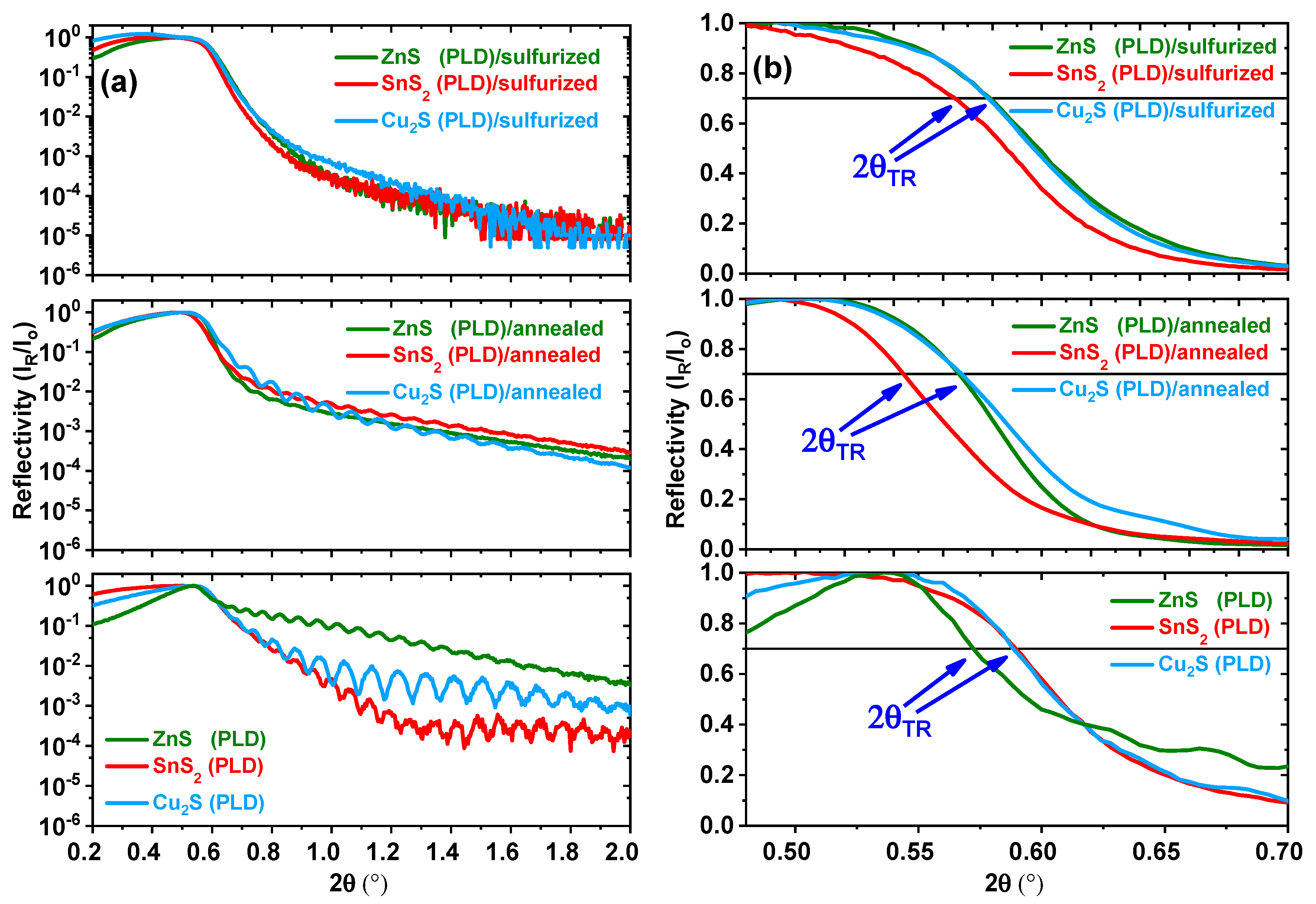
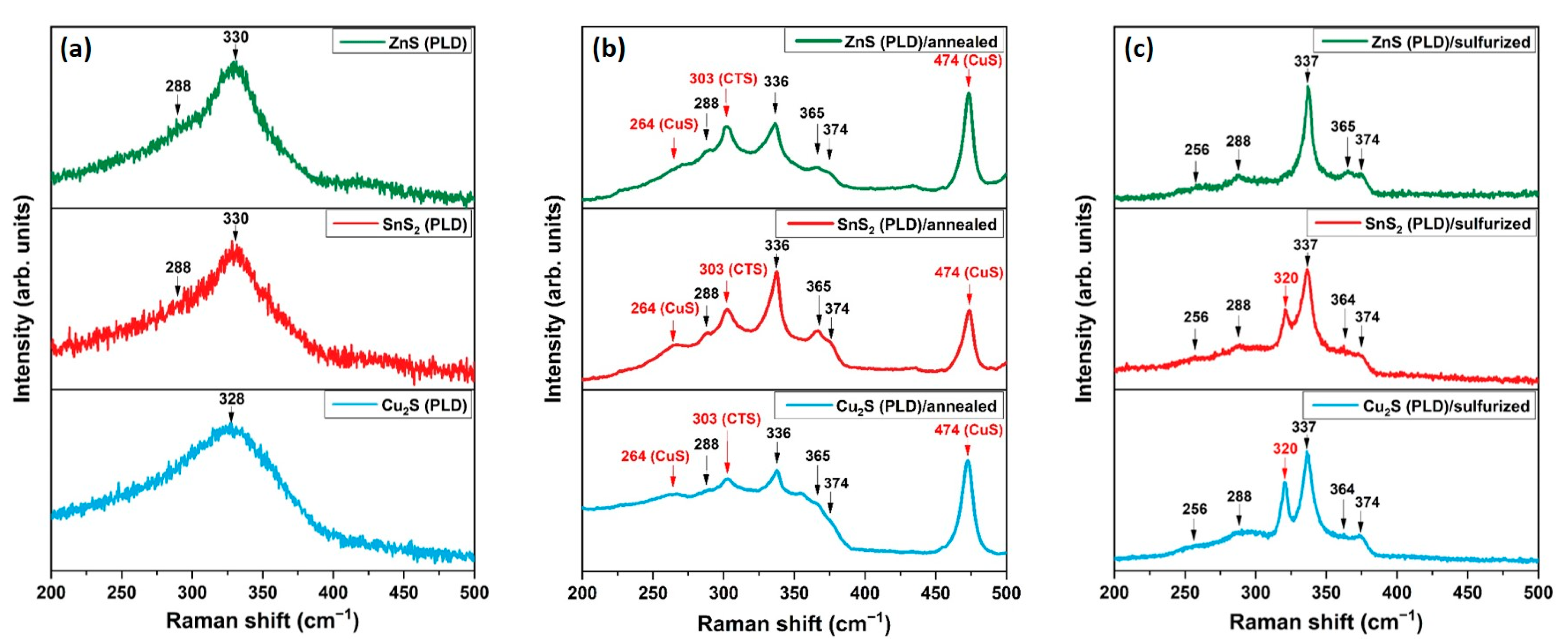
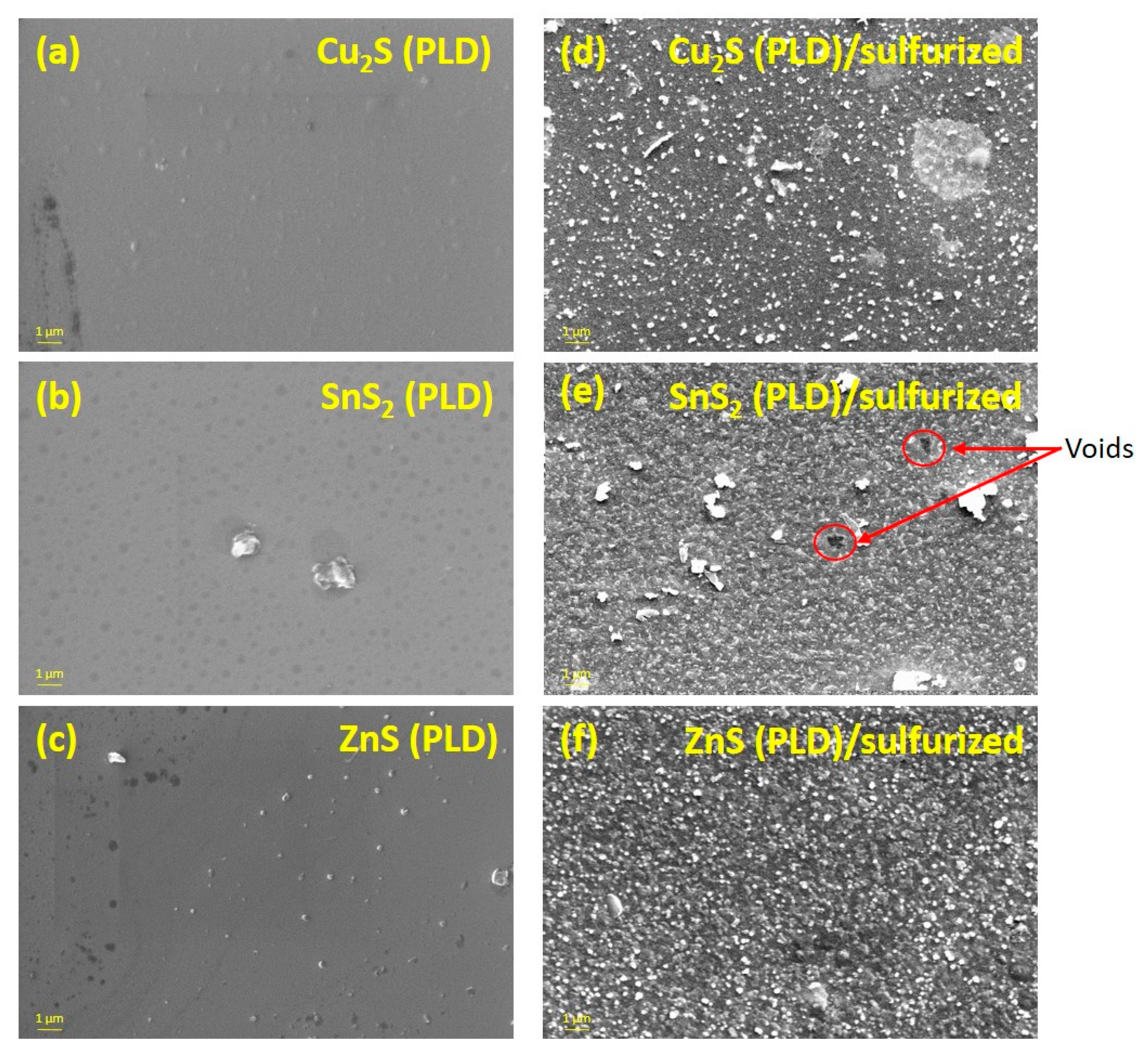
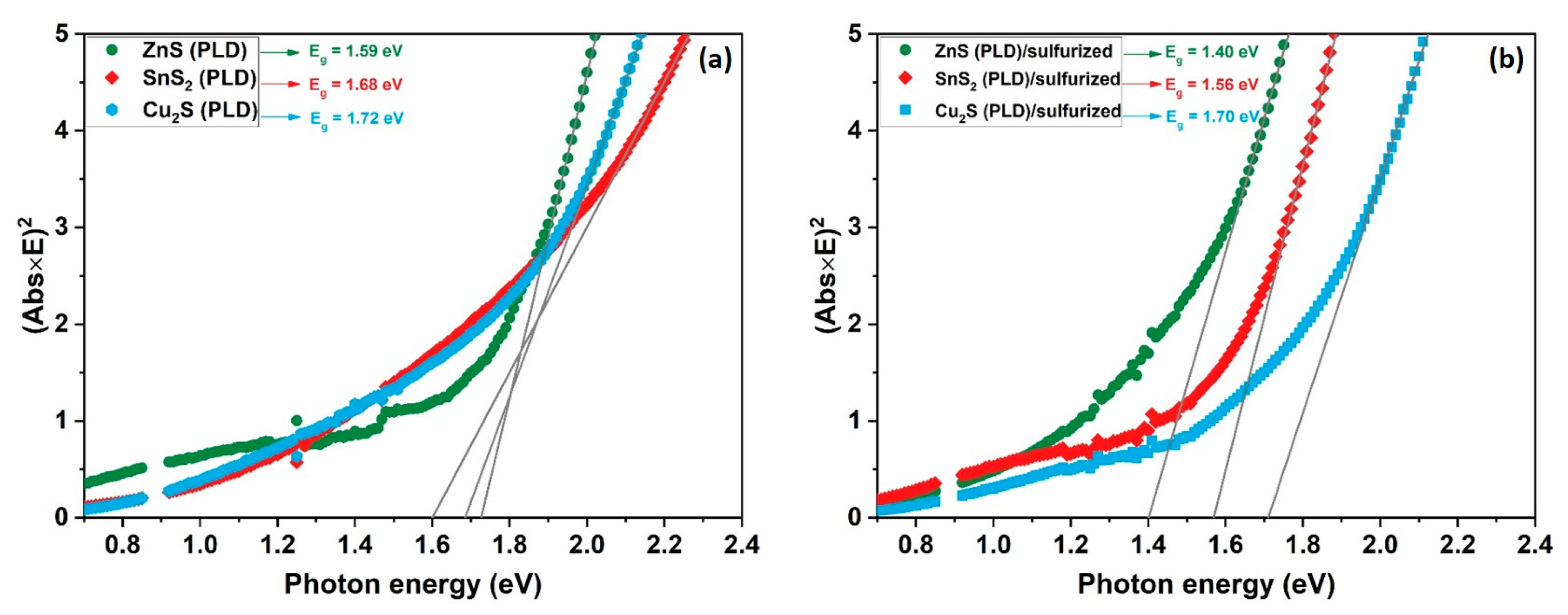
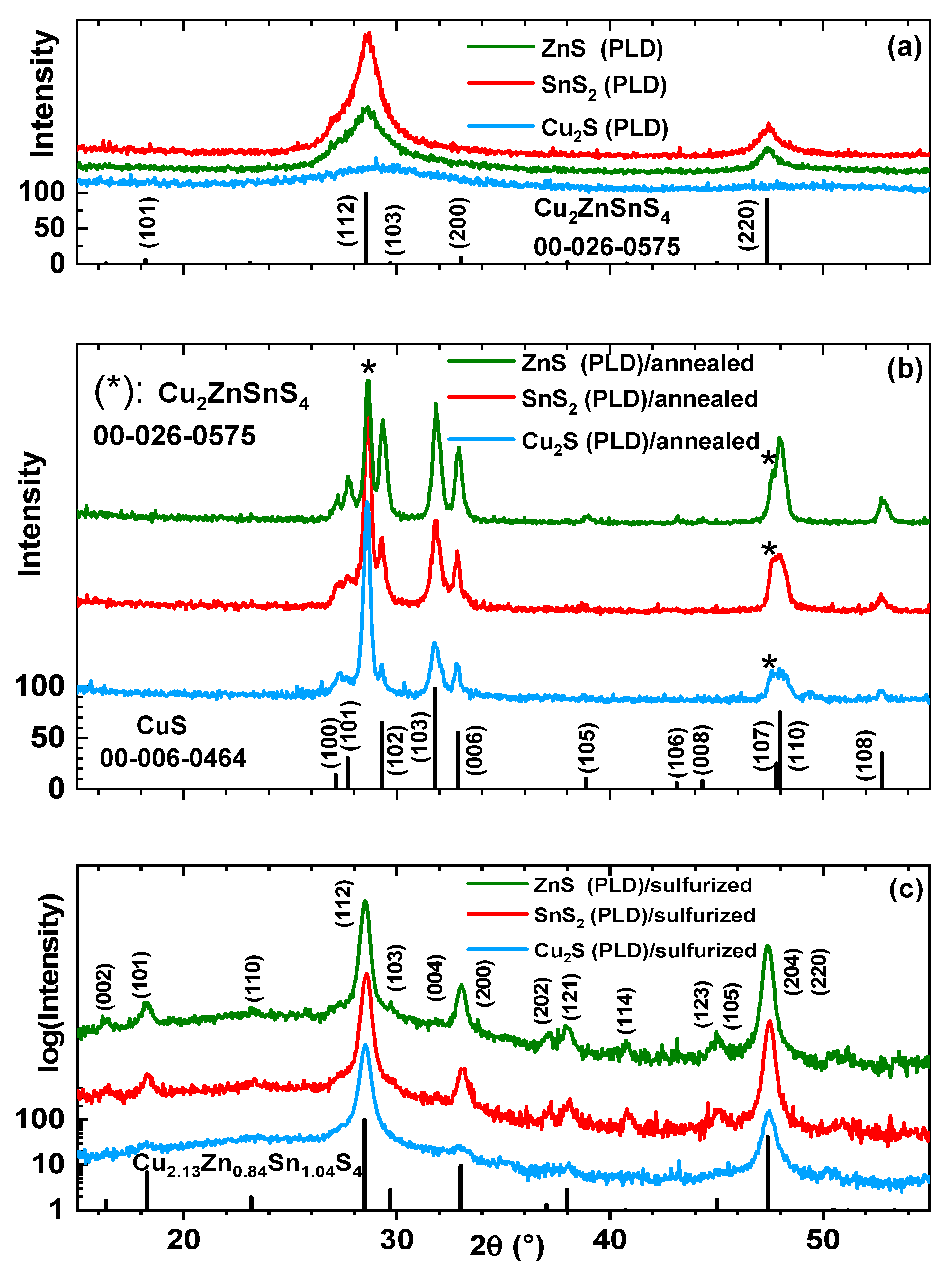
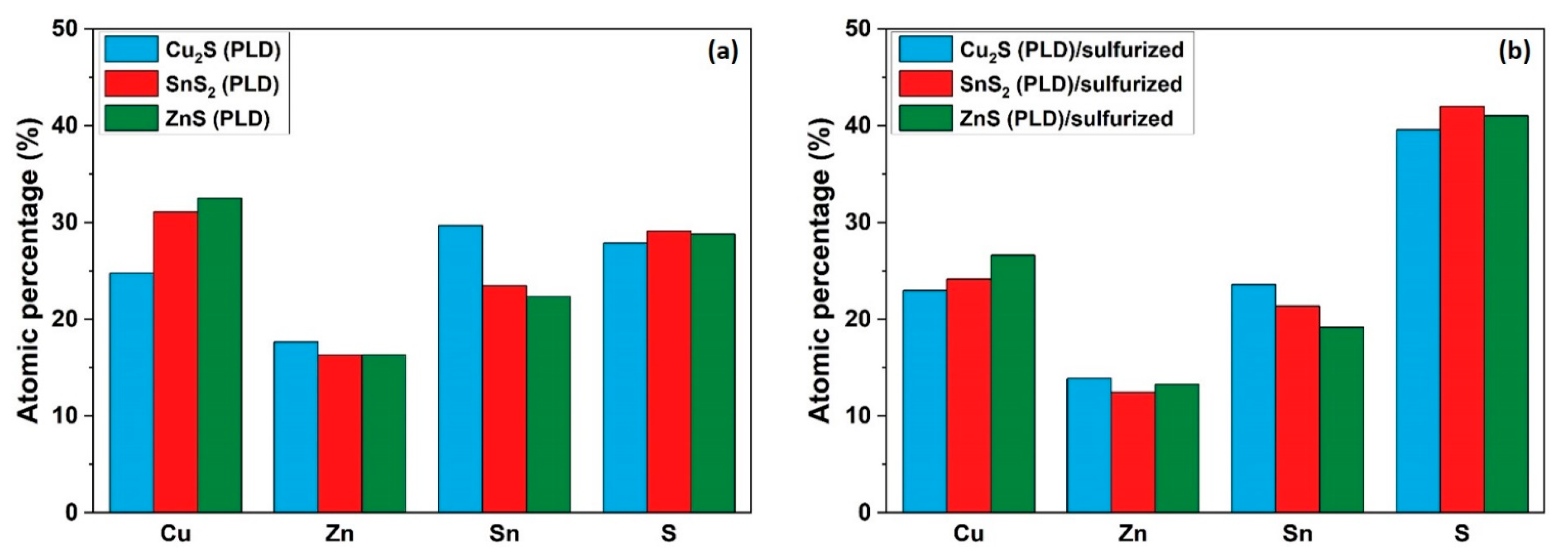
3. Results and Discussion

From the XRR diagrams of the three thin films obtained by MSPLD co-deposition, in the initial state and after annealing and sulfurization at 500 °C (Figure 1a), the positions of the total reflection edge (2θTR) (Figure 1b) and the average film thickness are calculated and presented in Table 1. The total reflection edge is defined as the angle for which the reflectivity decreases by 30% of the maximum. We notice that, after the heat treatment without sulfur, 2θTR decreases slightly for all the films. The average mass density (ρm) of the thin films is proportional with (θTR)2, and accordingly, ρm also decreases (Table 1). This fact, together with the decrease in the average thickness of all annealed CZTS thin films, means that the thin films undergo a process of partial evaporation and a reorganization of atoms, which produces the formation of voids between crystallites and a decrease in the thin-film thickness. The ZnS (PLD) thin film seems to be the least influenced by annealing without sulfur (both ρm and hm decrease with −2.1% and −2.0%, respectively), the mass loss being only −4.1%. SnS2 (PLD) is the most affected (both ρm and hm decrease with −14.7% and −14.3%, respectively), the mass loss being −29.0%. This might be due to the evaporation of the very volatile SnS [31] during the deposition and annealing. The Cu2S (PLD) thin film suffers moderate modifications (both ρm and hm decrease with −7.0% and −10.2%, respectively), the mass loss being −17.2%. The ZnS (PLD) sample is the densest and shows the smallest modifications in mass density and thickness after annealing. This could be due to the fact that in this case the deposition rate was double in comparison to the other two samples and the deposition rate influences the growth of the film (smoother films with smaller particle sizes are obtained at higher rates). When annealing with sulfur, the XRR fringes are not visible, meaning that the surface of the film becomes rough (confirmed by SEM), which is beneficial for solar cells. However, in this case, we expect a slight increase in the film thickness [32]. Additionally, the decrease in ρm is much diminished for Cu2S (PLD)/sulfurized and SnS2 (PLD)/sulfurized, while for ZnS (PLD)/sulfurized, ρm slightly increases, which means that the voids between crystallites are smaller than in the case of simple annealing.
Figure 2 shows the grazing incidence X-ray diffraction patterns of the CZTS thin films prepared using the MSPLD hybrid system by switching the target in the PLD carousel in each film and annealing without and with sulfur powder. The GIXRD diagrams for the as-deposited CZTS thin films are presented in Figure 2a. The Cu2S (PLD) sample has an amorphous structure, while for the SnS2 (PLD) and ZnS (PLD) samples, the amorphous phase is only 12% and 27%, respectively. The majority phase for the last two samples is polycrystalline Cu2ZnSnS4 (tetragonal, I-42m (121), as natural mineral “stannite”, ICDD file 00-026-0575) with an average size of crystallites of several nanometers. In order to prove the beneficial effect of sulfurization, we also annealed a set of samples without using sulfur. In this case (Figure 2b), all the samples suffer a major transformation: the amorphous phase and the Cu2ZnSnS4 nanophase (in the case of ZnS (PLD)/annealed and SnS2 (PLD)/annealed) are decomposed, some of the Zn and Sn atoms evaporate (thus the concentration of Cu atoms increase in thin films), the sulfur atoms diffuse in the entire volume of the thin films or evaporate (as XRR revealed), and thus, a polycrystalline CuS phase (hexagonal, P63/mmc (194), ICDD file 00-006-0464) appears. The average size of the crystallites for this phase is of hundreds of nanometers. Additionally, the average size of the crystallites for the remaining Cu2ZnSnS4 phase (tetragonal, I-42m (121), ICDD file 00-026-0575) increases to hundreds of nanometers. In Figure 2c are represented the GIXRD diagrams for the samples sulfurized at 500 °C. All the samples consist of a single phase, Cu2.13Zn0.84Sn1.04S4, with the tetragonal signature, the atomic plane (101), and some disorder distribution of the cations in the lattice (space group I-4 (82), similar to natural mineral “kesterite”, ICDD file 04-023-6314). The ZnS (PLD)/sulfurized sample appears to have sharper peaks than the other samples, suggesting an enhancement in crystallinity and particle growth after sulfurization [33]. Therefore, to confirm the suggested improvement, the average crystallite size D of the three sulfurized samples was calculated from the (112) peak of GIXRD data using the Scherrer formula: D = kλ/(β.cosθ), where D is the average crystallite size, k is the Scherrer constant, λ is the wavelength of Cu Kα, β is the corrected FWHM (by eliminating instrumental broadening) of the (112) peak, and θ is the Bragg angle. The D values are 69.40 nm for Cu2S (PLD)/sulfurized, 114.50 nm for SnS2 (PLD)/sulfurized, and the highest value of 153.24 nm for the ZnS (PLD)/sulfurized sample.
In order to confirm the results obtained by GIXRD, and to steadily identify the secondary phases in our samples, Raman spectroscopy was performed with an excitation wavelength of 633 nm. The effect of annealing without and with sulfur powder on the as-deposited thin films was studied and is presented in Figure 3. Two broad peaks at 288 cm−1 and 330 cm−1 are seen in all the as-deposited samples (Figure 3a). The main Raman peak of the kesterite CZTS phase is located at 336–338 cm−1 [34] but was reported to shift to lower values due to some disorder distribution of the cations in the lattice of the CZTS film [35]. Thus, these two peaks are identified as the characteristic peaks of the kesterite CZTS phase. Figure 3b shows the Raman spectra of the samples annealed without sulfur. CZTS peaks can be noticed in the three films at 288, 336, 365, and 374 cm−1 [36,37]; however, all the samples contain a strong peak at 474 cm−1 and a smaller one at 264 cm−1, indicating the presence of CuS [33]. In addition, a third phase is also detected in the films at 303 cm−1 and can be associated with the CTS phase [38]. The sulfurized CZTS thin films are presented in Figure 3c. Both the Cu2S (PLD)/sulfurized and SnS2 (PLD)/sulfurized samples are characterized by five peaks at 256, 288, 337, 364, and 374 cm−1 of the CZTS phase and a prominent peak at 320 cm−1 whose origin is unclear. Several researchers attributed this peak to the CTS [39,40] or SnS2 [41,42] secondary phases, while others stated that it belongs to CZTS [43,44]. On the other hand, the ZnS (PLD)/sulfurized sample contains peaks located at 256, 288, 337, 365, and 374 cm−1, which are uniquely characteristic of the CZTS phase [43,45], and no undesirable secondary phase was observed. As a side note, Raman measurements were also performed on all the samples using an excitation wavelength of 325 nm to detect the zinc sulfide phase [46], and no evidence of the ZnS or SnS2 secondary phases was detected. The annealing treatment either with or without sulfur plays a considerable role in the formation and crystallization of the CZTS films. However, a simple heat treatment without any sulfur source can lead to the apparition of several secondary phases, no matter what target was used for PLD, most probably due to the lack of sulfur and the very likely evaporation of zinc and tin in the form of SnS, resulting from the decomposition of SnS2 at high temperature [47]. As an alternative, sulfurization is primordial for synthesizing single-phase CZTS thin films, as observed in the ZnS (PLD)/sulfurized sample.
Figure 4 shows the SEM images of the as-deposited and sulfurized CZTS thin films. The surface of the as-deposited films (Figure 2a–c) is smooth, and no particles are observed. On the other hand, the surface of the films sulfurized at 500 °C (Figure 4d–f) is very rough, and agglomerations of hundreds of nanometers are visible. The Cu2S (PLD)/sulfurized sample (Figure 4d) is composed of a mixture of small and big particles. In Figure 4e, the SnS2 (PLD)/sulfurized sample exhibits a distribution of particles with different shapes and sizes along with some voids probably due to the evaporation of tin sulfide. The ZnS (PLD)/sulfurized film (Figure 4f) shows a more homogeneous and compact surface with monodispersed particles and no voids or cracks. The difference in particles sizes and shapes in the Cu2S (PLD)/sulfurized and SnS2 (PLD)/sulfurized samples can be explained by the co-existence of secondary phases [48], while a homogeneous surface with relatively monodispersed particles (ZnS (PLD)/sulfurized sample) suggests the existence of a single-phase compound, which further confirms the GIXRD and Raman results.
An estimation of the average atomic ratios of the four elements (Cu, Zn, Sn, and S), obtained from the energy-dispersive spectroscopy (EDS) analysis, in the as-deposited and sulfurized samples, is presented in Figure 5. All the as-prepared samples exhibit a Sn-rich and S-poor composition compared to the stoichiometric Cu2ZnSnS4 (Cu0.25Zn0.125Sn0.125S0.5) phase. By sulfurization at 500 °C, an improvement in the elemental composition is clearly seen in all the samples (Figure 5b), since the amounts of Cu, Zn, and Sn decreased, and the S quantity increased. However, the sulfurized samples are still off-stoichiometric, rich in tin, and slightly poor in sulfur. The existence of tin in excess can cause the formation of the SnS or SnS2 secondary phases [49]. This explains the apparition of the peak at 320 cm−1 in both samples (Cu2S (PLD)/sulfurized and SnS2 (PLD)/sulfurized) in the Raman analysis, which can be definitely attributed to the SnS2 phase. One should note that the determination of elemental concentrations by EDS can be affected by several parameters such as the sample thickness and the scattering power of atoms; therefore, significant errors are expected from this characterization technique [48].
The band gaps of the as-deposited and sulfurized CZTS thin films are shown in Figure 6. The transmittance measurements were performed using an ellipsometer, and the optical band gap was determined using the following equation [50]:
Abs(E) = ln (1/T) = C.d.√(E − Eg)
where Abs(E) is the derived absorbance using the measured transmittance (T), E is the photon energy, C is the constant of proportionality, d is the film thickness, and Eg is the optical band gap. Eg was estimated using the Tauc plot by plotting (αE)2 vs. (E) (where α is the absorption coefficient) near the absorption edge. Since the as-deposited samples in Figure 6a are mostly composed of an amorphous structure, the values of the optical band gaps are above the reported value for the CZTS thin films (≈1.5 eV). In Figure 6b are shown the band gaps of the CZTS sulfurized films. The estimated Eg is around 1.40, 1.56, and 1.70 eV for ZnS (PLD)/sulfurized, SnS2 (PLD)/sulfurized, and Cu2S (PLD)/sulfurized, respectively. The band gap is found to be correlated with the stoichiometry and the elemental composition of the CZTS material. Large Eg are caused by an increase in Sn content according to Malerba et al. [51], while Hamanaka et al. reported that the large values could be due to high Zn ratios along with a decrease in Cu content [52]. Eg also depends on the content of the three elements, more precisely on the Cu/(Zn + Sn) ratio, since higher energies are obtained with lower values of this ratio and vice versa [53]. This is confirmed in our case, as the Cu/(Zn + Sn) ratio in the Cu2S (PLD)/sulfurized sample is very small, and thus, a high value of the optical band gap (1.70 eV) is found. On the other hand, the ZnS (PLD)/sulfurized sample shows an enhancement in this ratio, leading to a lower band gap (1.40 eV). The optical properties of the CZTS thin films obtained here are in good agreement with the literature and are suitable for use in solar cells as absorber layers [54,55].
From the structural, morphological, compositional, and optical results, it can be deduced that the MSPLD hybrid system can be beneficial to the formation of the CZTS kesterite phase. This approach gives the possibility to produce rough films with larger crystallites when compared to some CZTS films prepared either by PLD [11] from a single Cu2ZnSnS4 target or by MS [17] from a quaternary CZTS alloy target. The XRD and Raman spectroscopy characterizations of the sulfurized films show the formation of a single CZTS crystalline phase in one set of samples (ZnS (PLD)/sulfurized) or the presence of one secondary phase (SnS2) in the other samples (SnS2 (PLD)/sulfurized and Cu2S (PLD)/sulfurized). On the other hand, CZTS absorber layers elaborated by MS can contain several secondary phases [21,56,57] such as Cu2S, CTS, and ZnS when multiple binary chalcogenide targets are used or even when a single alloyed CZTS target is sputtered, which can have a harmful impact on the performance of CZTS-based solar cells [58,59]. Additionally, one of the major drawbacks of the PLD method is the use of tiny substrates [60]. The problem can be solved and large-area substrates can be covered by implementing a hybrid MSPLD system that still benefits from PLD advantages. This can be helpful for large-scale industrial CZTS elaboration.

4. Conclusions

CZTS thin films were co-deposited simultaneously using three targets (Cu2S, SnS2, and ZnS) in a hybrid synthesis system combining magnetron sputtering (for two targets) and pulsed laser deposition (for the third target). The effect of the heat treatment with and without a sulfur atmosphere on the material properties was studied. The results show that a simple heat treatment without any sulfur source leads to the evaporation of Zn and Sn and the apparition of CuS and CTS secondary phases in all the films, no matter the target arrangement used. On the other hand, the sulfurized samples show that annealing in a sulfur atmosphere is an essential process for the formation of the CZTS phase. It is found that the samples obtained by simultaneous deposition of ZnS by PLD, Cu2S, and SnS2 by MS and sulfurized at 500 °C, which leads to the formation of a single-phase CZTS, have the best structural, compositional, and optical properties, confirmed by GIXRD, Raman, SEM-EDX, and transmission spectroscopy. For the other two sulfurized films, the SnS2 secondary phase is observed in both samples in the Raman analysis. The Cu2S (PLD)/sulfurized sample displays a wider band gap (1.70 eV) than the two other films, which have an optimal Eg (between 1.40 and 1.56 eV) for use as an absorber layer in CZTS-based solar cell applications. In fact, ZnS being deposited by PLD limits Zn loss during deposition and annealing and helps preserve an important amount of the ZnS phase required for the CZTS phase formation. In summary, the MSPLD hybrid technique is beneficial in obtaining high-quality CZTS thin films for use as absorber layers in solar cells.

Author Contributions

Conceptualization, M.-Y.Z., C.M. and A.V.; methodology, M.-Y.Z., A.-C.G. and A.V.; formal analysis, M.-Y.Z., F.S., A.-T.B., I.-D.S., A.-C.G. and A.V.; investigation, F.S., A.-T.B., M.-Y.Z., I.-D.S., N.B. and A.-C.G.; resources, A.V. and N.B.; writing—original draft preparation, M.-Y.Z., F.S., C.M. and A.V.; writing—review and editing, M.-Y.Z., F.S., C.M. and A.V.; visualization, M.-Y.Z., F.S. and C.M.; supervision, A.V.; project administration, A.-C.G. and A.V.; funding acquisition, A.-C.G. and A.V. All authors have read and agreed to the published version of the manuscript.

Funding

This work was supported by the Romanian Ministry of Research, Innovation and Digitalization in the framework of the POC-G 54/2016 MAT2IT (Contract No. 1550/2018) and PN-III-P4-ID-PCE-2020-0827 (Contract No. PCE74/09.02.2021) projects.

Data Availability Statement

The data presented in this study are available on a reasonable request from the corresponding author.

Conflicts of Interest

The authors declare no conflict of interest.

References

  1. Ahmoum, H.; Boughrara, M.; Su’ait, M.S.; Li, G.; Chopra, S.; Wang, Q.; Kerouad, M. Understanding the Effect of the Carbon on the Photovoltaic Properties of the Cu2ZnSnS4. Mater. Chem. Phys. 2020, 251, 123065. [Google Scholar] [CrossRef]
  2. Ataollahi, N.; Bazerla, F.; Malerba, C.; Chiappini, A.; Ferrari, M.; Di Maggio, R.; Scardi, P. Synthesis and Post-Annealing of Cu2ZnSnS4 Absorber Layers Based on Oleylamine/1-Dodecanethiol. Materials 2019, 12, 3320. [Google Scholar] [CrossRef] [Green Version]
  3. Sharmin, A.; Bashar, M.S.; Sultana, M.; Al Mamun, S.M.M. Sputtered Single-Phase Kesterite Cu2ZnSnS4 (CZTS) Thin Film for Photovoltaic Applications: Post Annealing Parameter Optimization and Property Analysis. AIP Adv. 2020, 10, 015230. [Google Scholar] [CrossRef] [Green Version]
  4. Song, X.; Ji, X.; Li, M.; Lin, W.; Luo, X.; Zhang, H. A Review on Development Prospect of CZTS Based Thin Film Solar Cells. Int. J. Photoenergy 2014, 2014, 1–11. [Google Scholar] [CrossRef]
  5. Vanalakar, S.A.; Agawane, G.L.; Shin, S.W.; Suryawanshi, M.P.; Gurav, K.V.; Jeon, K.S.; Patil, P.S.; Jeong, C.W.; Kim, J.Y.; Kim, J.H. A Review on Pulsed Laser Deposited CZTS Thin Films for Solar Cell Applications. J. Alloys Compd. 2015, 619, 109–121. [Google Scholar] [CrossRef]
  6. Zhu, Y.; Chen, Y.; Shen, T.; Yi, J.; Gan, G.; Huang, Q. Direct Current Magnetron Sputtered Cu2ZnSnS4 Thin Films Using a Ceramic Quaternary Target. J. Alloys Compd. 2017, 727, 1115–1125. [Google Scholar] [CrossRef]
  7. Whittles, T.J. Electronic Characterisation of Earth-Abundant Sulphides for Solar Photovoltaics; Springer Theses; Springer International Publishing: Cham, Switzerland, 2018; ISBN 978-3-319-91664-4. [Google Scholar] [CrossRef]
  8. Ogugua, S.N.; Ntwaeaborwa, O.M.; Swart, H.C. Latest Development on Pulsed Laser Deposited Thin Films for Advanced Luminescence Applications. Coatings 2020, 10, 1078. [Google Scholar] [CrossRef]
  9. Rath, M.; Varadarajan, E.; Natarajan, V.; Ramachandra Rao, M.S. A Comparative Study on Macroscopic and Nanoscale Polarization Mapping on Large Area PLD Grown PZT Thin Films. Ceram. Int. 2018, 44, 8749–8755. [Google Scholar] [CrossRef]
  10. Oulad Elhmaidi, Z.; Abd-Lefdil, M.; El Khakani, M.A. Photoconversion Optimization of Pulsed-Laser-Deposited p-CZTS/n-Si-Nanowires Heterojunction-Based Photovoltaic Devices. Nanomaterials 2020, 10, 1393. [Google Scholar] [CrossRef]
  11. Oulad Elhmaidi, Z.; Pandiyan, R.; Abd-Lefdil, M.; El Khakani, M.A. Pulsed Laser Deposition of CZTS Thin Films, Their Thermal Annealing and Integration into n-Si/CZTS Photovoltaic Devices. In Proceedings of the 2016 International Renewable and Sustainable Energy Conference (IRSEC) 2016, Marrakech, Morocco, 14–17 November 2016; pp. 130–135. [Google Scholar] [CrossRef]
  12. Cazzaniga, A.; Crovetto, A.; Yan, C.; Sun, K.; Hao, X.; Ramis Estelrich, J.; Canulescu, S.; Stamate, E.; Pryds, N.; Hansen, O.; et al. Ultra-Thin Cu2ZnSnS4 Solar Cell by Pulsed Laser Deposition. Sol. Energy Mater. Sol. Cells 2017, 166, 91–99. [Google Scholar] [CrossRef] [Green Version]
  13. Ettlinger, R.B.; Crovetto, A.; Canulescu, S.; Cazzaniga, A.; Ravnkilde, L.; Youngman, T.; Hansen, O.; Pryds, N.; Schou, J. Formation of Copper Tin Sulfide Films by Pulsed Laser Deposition at 248 and 355 Nm. Appl. Phys. A 2016, 122, 466. [Google Scholar] [CrossRef] [Green Version]
  14. Cazzaniga, A.; Ettlinger, R.B.; Canulescu, S.; Schou, J.; Pryds, N. Nanosecond Laser Ablation and Deposition of Silver, Copper, Zinc and Tin. Appl. Phys. A 2014, 117, 89–92. [Google Scholar] [CrossRef]
  15. Noroozi, M.; Petruhins, A.; Greczynski, G.; Rosen, J.; Eklund, P. Structural and Mechanical Properties of Amorphous AlMgB14 Thin Films Deposited by DC Magnetron Sputtering on Si, Al2O3 and MgO Substrates. Appl. Phys. A 2020, 126, 133. [Google Scholar] [CrossRef] [Green Version]
  16. Olgar, M.A.; Klaer, J.; Mainz, R.; Levcenco, S.; Just, J.; Bacaksiz, E.; Unold, T. Effect of Precursor Stacking Order and Sulfurization Temperature on Compositional Homogeneity of CZTS Thin Films. Thin Solid Film. 2016, 615, 402–408. [Google Scholar] [CrossRef]
  17. Jheng, B.-T.; Liu, P.-T.; Wu, M.-C. A Promising Sputtering Route for Dense Cu2ZnSnS4 Absorber Films and Their Photovoltaic Performance. Sol. Energy Mater. Sol. Cells 2014, 128, 275–282. [Google Scholar] [CrossRef]
  18. Xie, M.; Zhuang, D.; Zhao, M.; Zhuang, Z.; Ouyang, L.; Li, X.; Song, J. Preparation and Characterization of a Cu2ZnSnS4 Thin Films and Solar Cells Fabricated from Quaternary Cu-Zn-Sn-S Target. Int. J. Photoenergy 2013, 2013, 929454. [Google Scholar] [CrossRef]
  19. Olgar, M.A.; Klaer, J.; Mainz, R.; Ozyuzer, L.; Unold, T. Cu2ZnSnS4-Based Thin Films and Solar Cells by Rapid Thermal Annealing Processing. Thin Solid Film. 2017, 628, 1–6. [Google Scholar] [CrossRef]
  20. Behera, N.; Mohan, D.B. The Phase Optimization, Optical and Electrical Properties of Kesterite Cu2ZnSnS4 Thin Film Prepared by Single Target RF Magnetron Sputtering Technique for Solar Cell Application. Mater. Res. Express 2020, 6, 126457. [Google Scholar] [CrossRef]
  21. Rudisch, K.; Davydova, A.; Riekehr, L.; Adolfsson, J.; Quaglia Casal, L.; Platzer-Björkman, C.; Scragg, J. Prospects for Defect Engineering in Cu2ZnSnS4 Solar Absorber Films. J. Mater. Chem. A 2020, 8, 15864–15874. [Google Scholar] [CrossRef]
  22. Rondiya, S.; Rokade, A.; Jadhavar, A.; Nair, S.; Chaudhari, M.; Kulkarni, R.; Mayabadi, A.; Funde, A.; Pathan, H.; Jadkar, S. Effect of Calcination Temperature on the Properties of CZTS Absorber Layer Prepared by RF Sputtering for Solar Cell Applications. Mater. Renew. Sustain. Energy 2017, 6, 8. [Google Scholar] [CrossRef] [Green Version]
  23. Zhao, H.; Xie, J.; Mao, A. Effects of Bottom Layer Sputtering Pressures and Annealing Temperatures on the Microstructures, Electrical and Optical Properties of Mo Bilayer Films Deposited by RF/DC Magnetron Sputtering. Appl. Sci. 2019, 9, 1395. [Google Scholar] [CrossRef] [Green Version]
  24. Khalkar, A.; Lim, K.-S.; Yu, S.-M.; Patole, S.P.; Yoo, J.-B. Deposition of Cu2ZnSnS4 Thin Films by Magnetron Sputtering and Subsequent Sulphurization. Electron. Mater. Lett. 2014, 10, 43–49. [Google Scholar] [CrossRef]
  25. Gudmundsson, J.T. Physics and Technology of Magnetron Sputtering Discharges. Plasma Sources Sci. Technol. 2020, 29, 113001. [Google Scholar] [CrossRef]
  26. Alvarez, R.; Garcia-Valenzuela, A.; Lopez-Santos, C.; Ferrer, F.J.; Rico, V.; Guillen, E.; Alcon-Camas, M.; Escobar-Galindo, R.; Gonzalez-Elipe, A.R.; Palmero, A. High-Rate Deposition of Stoichiometric Compounds by Reactive Magnetron Sputtering at Oblique Angles. Plasma Process. Polym. 2016, 13, 960–964. [Google Scholar] [CrossRef] [Green Version]
  27. Benetti, D.; Nouar, R.; Nechache, R.; Pepin, H.; Sarkissian, A.; Rosei, F.; MacLeod, J.M. Combined Magnetron Sputtering and Pulsed Laser Deposition of TiO2 and BFCO Thin Films. Sci. Rep. 2017, 7, 2503. [Google Scholar] [CrossRef] [Green Version]
  28. Gómez-Solano, R.E.; Arias-Cerón, J.S.; Ríos-Ramírez, J.J.; Ortega-López, M. Synthesis and Study of Structure and Phase Composition in Cu2–XS, SnxSy, ZnS, CuxSnSy and CuZnSnS Pellets. J. Mater. Sci. Mater. Electron. 2020, 31, 7519–7523. [Google Scholar] [CrossRef]
  29. Al-Hadeethi, Y.; Mkawi, E.M.; Al-Hartomy, O.; Bekyarova, E. Solvothermal Synthesis of Kesterite Cu2ZnSnS4 Nanocrystals: Influence of Glycine Complexing Agent Concentration on Properties. Ceram. Int. 2021, 47, 11568–11573. [Google Scholar] [CrossRef]
  30. Simandan, I.-D.; Sava, F.; Buruiana, A.-T.; Galca, A.-C.; Becherescu, N.; Burducea, I.; Mihai, C.; Velea, A. Influence of Deposition Method on the Structural and Optical Properties of Ge2Sb2Te5. Materials 2021, 14, 3663. [Google Scholar] [CrossRef] [PubMed]
  31. Huang, L.; Li, J.; Wang, S.; Zhong, L.; Xiao, X. Forming an Ultrathin SnS Layer on Cu 2 ZnSnS 4 Surface to Achieve Highly Efficient Solar Cells with Zn(O,S) Buffer. Solar RRL 2020, 4, 2000010. [Google Scholar] [CrossRef]
  32. Tao, J.; Liu, J.; He, J.; Zhang, Z.; Jiang, J.; Sun, L.; Yang, P.; Chu, J. Synthesis and characterization of Cu2ZnSnS4 thin films by the sulfurization of co-electrodeposited Cu–Zn–Sn–S precursor layers for solar cell applications. RSC Adv. 2014, 4, 23977–23984. [Google Scholar] [CrossRef]
  33. Engberg, S.; Symonowicz, J.; Schou, J.; Canulescu, S.; Jensen, K.M.Ø. Characterization of Cu2ZnSnS4 Particles Obtained by the Hot-Injection Method. ACS Omega 2020, 5, 10501–10509. [Google Scholar] [CrossRef]
  34. Havryliuk, Y.; Valakh, M.Y.; Dzhagan, V.; Greshchuk, O.; Yukhymchuk, V.; Raevskaya, A.; Stroyuk, O.; Selyshchev, O.; Gaponik, N.; Zahn, D.R.T. Raman characterization of Cu2ZnSnS4 nanocrystals: Phonon confinement effect and formation of CuxS phases. RSC Adv. 2018, 8, 30736. [Google Scholar] [CrossRef] [Green Version]
  35. Lin, J.; Xu, J.; Yang, Y. Effect of Sulfur Powder Mass on the Formation of MoS2 Interface Layer between Cu2ZnSnS4 Thin Film and Mo Foil. Superlattices Microstruct. 2020, 147, 106724. [Google Scholar] [CrossRef]
  36. Azmi, S.; Moujib, A.; Layachi, O.A.; Matei, E.; Galca, A.C.; Zaki, M.Y.; Secu, M.; Rusu, M.I.; Grigorescu, C.E.A.; Khoumri, E.M. Towards Phase Pure Kesterite Cu2ZnSnS4 Absorber Layers Growth via Single Step Free Sulfurization Electrodeposition under a Fix Applied Potential on Mo Substrate. J. Alloys Compd. 2020, 842, 155821. [Google Scholar] [CrossRef]
  37. Dimitrievska, M.; Fairbrother, A.; Fontane, X.; Jawhari, T.; Izquierdo-Roca, V.; Saucedo, E.; Perez-Rodriguez, A. Multiwavelength excitation Raman scattering study of polycrystalline kesterite Cu2ZnSnS4 thin films. Appl. Phys. Lett. 2014, 104, 021901. [Google Scholar] [CrossRef] [Green Version]
  38. Chaudhari, J.J.; Joshi, U.S. Fabrication of high quality Cu2SnS3 thin film solar cell with 1.12% power conversion efficiency obtain by low cost environment friendly sol-gel technique. Mater. Res. Express 2018, 5, 036203. [Google Scholar] [CrossRef]
  39. Kumar, M.; Dubey, A.; Adhikari, N.; Venkatesan, S.; Qiao, Q. Strategic Review of Secondary Phases, Defects and Defect-Complexes in Kesterite CZTS–Se Solar Cells. Energy Environ. Sci. 2015, 8, 3134–3159. [Google Scholar] [CrossRef]
  40. Tan, J.M.R.; Lee, H.; Pedireddy, S.; Baikie, T.; Ling, X.Y.; Wong, L.H. Understanding the Synthetic Paterhway of a Single-Phase Quaternary Semiconductor Using Surface-Enhanced Raman Scattering: A case of Wurtzite Cu2ZnSnS4 Nanoparticles. J. Am. Chem. Soc. 2014, 136, 6684–6692. [Google Scholar] [CrossRef] [PubMed]
  41. Ahmad, R.; Brandl, M.; Distaso, M.; Herre, P.; Spiecker, E.; Hock, R.; Peukert, W. A comprehensive study on the mechanism behind formation and depletion of Cu2ZnSnS4 (CZTS) phases. Cryst. Eng. Comm. 2015, 17, 6972–6984. [Google Scholar] [CrossRef] [Green Version]
  42. Isik, M.; Gullu, H.H.; Terlemezoglu, M.; Bayrakli Surucu, O.; Parlak, M.; Gasanly, N.M. Investigation of Band Gap Energy Versus Temperature for SnS2 thin films grown by RF-Magnetron Sputtering. Phys. B 2020, 591, 412264. [Google Scholar] [CrossRef]
  43. Dimitrievska, M.; Boero, F.; Litvinchuk, A.P.; Delsante, S.; Borzone, G.; Perez-Rodriguez, A.; Izquierdo-Roca, V. Structural Polymorphism in “Kesterite” Cu2ZnSnS4: Raman Spectroscopy and First-Principles Calculations Analysis. Inorg. Chem. 2017, 56, 3467–3474. [Google Scholar] [CrossRef] [PubMed]
  44. Guc, M.; Levcenko, S.; Bodnar, I.V.; Izquierdo-Roca, V.; Fontane, X.; Volkova, L.V.; Arushanov, E.; Perez-Rodriguez, A. Polarized Raman Scattering Study of Kesterite Type Cu2ZnSnS4 Single Crystals. Sci. Rep. 2016, 6, 19414. [Google Scholar] [CrossRef] [Green Version]
  45. Sava, F.; Diagne, O.; Galca, A.-C.; Simandan, I.-D.; Matei, E.; Burdusel, M.; Becherescu, N.; Becherescu, V.; Mihai, C.; Velea, A. Secondary Crystalline Phases Influence on Optical Properties in Off-Stoichiometric Cu2S–ZnS–SnS2 Thin Films. Materials 2020, 13, 4624. [Google Scholar] [CrossRef]
  46. Chen, R.; Fan, J.; Li, H.; Liu, C.; Mai, Y. Efficiency Enhancement of Cu2ZnSnS4 Solar Cells via Surface Treatment Engineering. R Soc. Open Sci. 2018, 5. [Google Scholar] [CrossRef] [Green Version]
  47. Wang, W.; Chen, G.; Cai, H.; Chen, B.; Yao, L.; Yang, M.; Chen, S.; Huang, Z. The Effects of SnS2 Secondary Phases on Cu2ZnSnS4 Solar Cells: A Promising Mechanical Exfoliation Method for Its Removal. J. Mater. Chem. A 2018, 6, 2995–3004. [Google Scholar] [CrossRef]
  48. Zaki, M.Y.; Nouneh, K.; Ebn Touhami, M.; Belakhmima, R.A.; Galca, A.C.; Pintilie, L.; Enculescu, M.; Baibarac, M.; Taibi, M. Effect of Mixing Complexing Agents on the Properties of Electrodeposited CZTS Thin Films. Opt. Mater. 2018, 83, 252–256. [Google Scholar] [CrossRef]
  49. Wang, H.; Yasin, A.; Quitoriano, N.J.; Demopoulos, G.P. Aqueous-based Binary Sulfide Nanoparticle Inks for Cu2ZnSnS4 Thin Films Stabilized with Tin(IV) Chalcogenide Complexes. Nanomaterials 2019, 9, 1382. [Google Scholar] [CrossRef] [PubMed] [Green Version]
  50. El Khouja, O.; Galca, A.C.; Nouneh, K.; Zaki, M.Y.; Ebn Touhami, M.; Taibi, M.; Matei, E.; Negrila, C.C.; Enculescu, M.; Pintilie, L. Structural, Morphological and Optical Properties of Cu–Fe–Sn–S Thin Films Prepared by Electrodeposition at Fixed Applied Potential. Thin Solid Film. 2021, 721, 138547. [Google Scholar] [CrossRef]
  51. Malerba, C.; Biccari, F.; Azanza Ricardo, C.L.; Valentini, M.; Chierchia, R.; Müller, M.; Santoni, A.; Esposito, E.; Mangiapane, P.; Scardi, P.; et al. CZTS Stoichiometry Effects on the Band Gap Energy. J. Alloys Compd. 2014, 582, 528–534. [Google Scholar] [CrossRef]
  52. Hamanaka, Y.; Oyaizu, W.; Kawase, M.; Kuzuya, T. Synthesis of Highly Non-Stoichiometric Cu2ZnSnS4 Nanoparticles with Tunable Bandgaps. J. Nanopart Res. 2017, 19, 9. [Google Scholar] [CrossRef]
  53. Elhmaidi, Z.O.; Pandiyan, R.; Abd-Lefdil, M.; Saucedo, E.; El Khakani, M.A. In-Situ Tuning of the Zinc Content of Pulsed-Laser-Deposited CZTS Films and Its Effect on the Photoconversion Efficiency of p-CZTS/n-Si Heterojunction Photovoltaic Devices. Appl. Surf. Sci. 2020, 507, 145003. [Google Scholar] [CrossRef]
  54. Aldalbahi, A.; Mkawi, E.M.; Ibrahim, K.; Farrukh, M.A. Effect of Sulfurization Time on the Properties of Copper Zinc Tin Sulfide Thin Films Grown by Electrochemical Deposition. Sci. Rep. 2016, 6, 32431. [Google Scholar] [CrossRef] [Green Version]
  55. Zhang, X.; Fu, E.; Wang, Y.; Zhang, C. Fabrication of Cu2ZnSnS4 (CZTS) Nanoparticle Inks for Growth of CZTS Films for Solar Cells. Nanomaterials 2019, 9, 336. [Google Scholar] [CrossRef] [PubMed] [Green Version]
  56. Chawla, V.; Clemens, B. Effect of composition on high efficiency CZTSSe devices fabricated using co-sputtering of compound targets. In Proceedings of the 2012 38th IEEE Photovoltaic Specialists Conference, Austin, TX, USA, 3–8 June 2012; pp. 002990–002992. [Google Scholar] [CrossRef]
  57. Hlaing Oo, W.; Johnson, J.; Bhatia, A.; Lund, E.-A.; Nowell, M.-M.; Scarpulla, M.-A. Grain Size and Texture of Cu2ZnSnS4 Thin Films Synthesized by Cosputtering Binary Sulfides and Annealing: Effects of Processing Conditions and Sodium. J. Electron. Mater. 2011, 40, 2214. [Google Scholar] [CrossRef]
  58. Bao, W.; Ichimura, M. Influence of Secondary Phases in Kesterite-Cu2ZnSnS4 Absorber Material Based on the First Principles Calculation. Int. J. Photoenergy 2015, 2015, 592079. [Google Scholar] [CrossRef] [Green Version]
  59. Liu, W.-S.; Chen, S.-Y.; Huang, C.-S.; Lee, M.-Y.; Kuo, H.-C. Investigation of Zn/Sn ratio for improving the material quality of CZTS thin films with the reduction of Cu2-xS secondary phase. J. Alloys Compd. 2020, 853, 157237. [Google Scholar] [CrossRef]
  60. Muhunthan, N.; Singh, O.P.; Singh, S.; Singh, V.N. Growth of CZTS Thin Films by Cosputtering of Metal Targets and Sulfurization in H2S. Int. J. Photoenergy 2013, 2013, 752012. [Google Scholar] [CrossRef] [Green Version]
Figure 1. (a) XRR diagrams for co-deposited CZTS thin films in the as-deposited state, after annealing at 500 °C and after sulfurization at 500 °C. (b) Positions of the total reflection edge (2θTR), defined as the angle for which the reflectivity decreases by 30% of the maximum.
Nanomaterials 11 02403 g001
Figure 2. Grazing incidence X-Ray diffraction patterns of the MSPLD thin films (a) as-deposited, (b) annealed at 500 °C, and (c) sulfurized at 500 °C.
Nanomaterials 11 02403 g002
Figure 3. Raman spectra of the MSPLD samples (a) as-deposited, (b) annealed without sulfur at 500 °C, and (c) sulfurized at 500 °C.
Nanomaterials 11 02403 g003
Figure 4. Surface SEM images of the samples on glass substrate as-deposited and sulfurized: (a) Cu2S (PLD), (b) SnS2 (PLD), and (c) ZnS (PLD) (as-deposited); (d) Cu2S (PLD)/sulfurized, (e) SnS2 (PLD)/sulfurized, and (f) ZnS (PLD)/sulfurized (sulfurized).
Nanomaterials 11 02403 g004
Figure 5. Average atomic ratios of Cu, Zn, Sn and S in the samples obtained in the hybrid MSPLD deposition system: (a) as-deposited and (b) sulfurized.
Nanomaterials 11 02403 g005
Figure 6. Tauc plot of the (a) as-deposited and (b) sulfurized CZTS thin films.
Nanomaterials 11 02403 g006
Table 1. Position of the total reflection edge (2θTR) and the average thickness (hm) (as well as their relative variation) of the as-deposited, annealed, and sulfurized CZTS thin films.
TR; Δρmohm (nm); Δhm/ho
SampleAs-DepositedAnnealed @ 500 °CSulfurized @ 500 °CAs-DepositedAnnealed @ 500 °CSulfurized @ 500 °C
ZnS (PLD)0.572°0.566°; −2.1%0.579; +2.5%145142; −2.0%-
SnS2 (PLD)0.589° 0.544°; −14.7%0.565; +8.0%147 126; −14.3%-
Cu2S (PLD)0.588°0.567°; −7.0%0.578; +3.4%108 97; −10.2%-
Publisher’s Note: MDPI stays neutral with regard to jurisdictional claims in published maps and institutional affiliations.

