Article

A Scalable Solution Route to Porous Networks of Nanostructured Black Tungsten

1
School of Chemical, Biological and Environmental Engineering, Oregon State University, Corvallis, OR 97331, USA
2
School of Mechanical, Industrial and Manufacturing Engineering, Oregon State University, Corvallis, OR 97331, USA
3
Advanced Technology and Manufacturing Institute (ATAMI), Corvallis, OR 97330, USA
*
Author to whom correspondence should be addressed.
Nanomaterials 2021, 11(9), 2304; https://doi.org/10.3390/nano11092304
Submission received: 18 August 2021 / Revised: 29 August 2021 / Accepted: 31 August 2021 / Published: 5 September 2021
(This article belongs to the Special Issue Scalable Fabrication of Nanostructured Materials and Devices)

Abstract

:
This paper studied the feasibility of a new solution-processed method to manufacture black tungsten nanostructures by laser conversion of tungsten hexacarbonyl precursor on the Inconel 625 substrate under argon atmosphere at ambient pressure. The results show that sublimation of the precursor can be prevented if the decomposition temperature (>170 °C) is achieved using the laser heating method. Three different laser powers from 60–400 W were used to investigate the role of laser parameters on the conversion. It was found that lower laser power of 60 W resulted in a mixture of unconverted precursor and converted tungsten. Higher laser powers >200 W resulted in α-W (BCC) in one step without further heat treatment. Different oxygen concentrations from 0.5 ppm to 21 vol% were used in the laser canister to investigate the effect of oxygen concentration on the conversion. It was found that the hard vacuum (>10−4 torr) or hydrogen is not necessary to obtain α-W (BCC). The solar absorptance varied from 63–97%, depending on the amount of precursor deposited on the substrate and oxygen content in the laser canister. This solution-based laser conversion of tungsten precursor is a scalable method to manufacture tungsten coatings for high-temperature applications.

1. Introduction

Tungsten, the highest melting point element known in the periodic table, with low thermal expansion coefficient, good thermal and electrical conductivity, wear-resistance, and chemical stability, has a wide range of applications, such as ohmic contacts, interconnects, solar thermal absorbers, IR reflectors, diffusion barriers, and high-strength metal matrix composites [1,2,3,4]. One growing use of W is as a high-temperature, absorber layer to increase the solar absorptivity and decrease the thermal emissivity of solar thermal collectors or receivers for various energy applications [1,5,6,7]. Particularly, creating plasmonic nanostructured metals (nanorods, nanoparticles, nanoporous films) is of great interest as they augment the absorption of electromagnetic radiation over a tunable range of UV to near IR [8,9]. Different synthesis methods have been used to manufacture W films and coatings capable of modifying the solar absorptance of these surfaces. Gesheva et al. [10] deposited black W films by chemical vapor deposition (CVD) of tungsten hexacarbonyl (W(CO)6) under hydrogen atmosphere for photothermal solar energy conversion applications. Shah et al. [9] manufactured a spectrally selective solar absorber by laser sintering of W micro and nanoparticles on stainless steel (SS) substrate with a solar absorptance of 83% and emissivity of 11.6%. Sibin et al. [4] manufactured IR-reflective W films by magnetron sputtering to control the thermal emittance of stainless steel substrates. Gao et al. [1] produced surface textured W with enhanced absorption of 74% and reduced emittance of 5%. They observed increased solar absorptance of 0.9 with SS/W/Al2O3 tandem coatings. Salama et al. [11] developed a better gamma shielding capability of SS316 alloy by replacing Mo with W.
Paul et al. [12] developed a hybrid metal additive manufacturing process that exploits liquid ink-jetting (drop on demand) into the powder bed to manufacture metal alloys. This method is capable of direct printing of alloys that are difficult to process via conventional powder metallurgy routes such as oxide dispersion strengthened alloys. It can also manufacture materials with spatially tailored properties (such as functionally graded alloys). Producing W-based metal matrix composites such as W-austenitic SS [11], W-reinforced Al matrix [2], and Cu-W composites [13,14] by hybrid metal additive manufacturing (AM) would be very beneficial for a wide range of applications.
Despite the potential for utilizing W films, coatings, and patterns for a wide variety of applications, there are very few studies of solution processing methods of W films and coatings. One such study produced metallic W films by spin coating peroxopolytungstic acid [15]. This spin coating method indirectly produces W by reducing the tungsten oxide films made from the precursor. Nonetheless, the implementation of scalable manufacturing is a significant challenge. Aerosol jet printing (AJP) is an AM technique that enables the large-scale manufacturing of films, coatings, and devices. It is a versatile method that uses inks with a wide range of rheological properties [16].
Nevertheless, a significant challenge to develop inks containing W is the precursor solubility and their reaction chemistry. Some of the organometallic precursors being used for CVD and atomic layer deposition (ALD) approaches to depositing W films include tungsten hexafluoride (WF6) and tungsten hexachloride (WCl6). However, they require strong reducing agents such as H2 and silane gas to reduce these halide precursors to metallic tungsten. In addition, the byproduct gases are corrosive and thus not desirable. W(CO)6 is another widely used metal-organic precursor because of its volatile nature, and it decomposes into W and CO gas at temperatures >170 °C in an inert atmosphere. It has been a precursor choice to produce W films by CVD and laser-induced CVD [3,10,17].
This paper presents the feasibility of using a molecular precursor (W(CO)6) ink dissolved in a solvent to manufacture nanostructured W coatings using laser conversion. This new solution-based method entails scalability, pre-printing the precursor patterns onto a surface of interest, and converting it later using the laser. Additionally, this process opens avenues to manufacturing W-based functionally graded materials and tailored alloys using hybrid metal additive manufacturing processes. Prior to the printing, the feasibility of converting the sublimable precursor directly without sublimating the precursor was studied. Morphology, crystal structure, composition, and solar absorptance of produced W coatings were also analyzed.

2. Materials and Methods

2.1. Materials

Tungsten hexacarbonyl (99% pure, 0.3% Mo, Strem Chemicals) and tetrahydrofuran (THF, >99.9%, fisher chemical) were used as a precursor and solvent, respectively. We prepared 0.071 M ink by adding the precursor to THF and ultrasonicated for 15 min. Inconel 625 substrates, purchased from McMaster-Carr, were polished using emery paper and cleaned with acetone, methanol, and DI water before depositing the precursor.

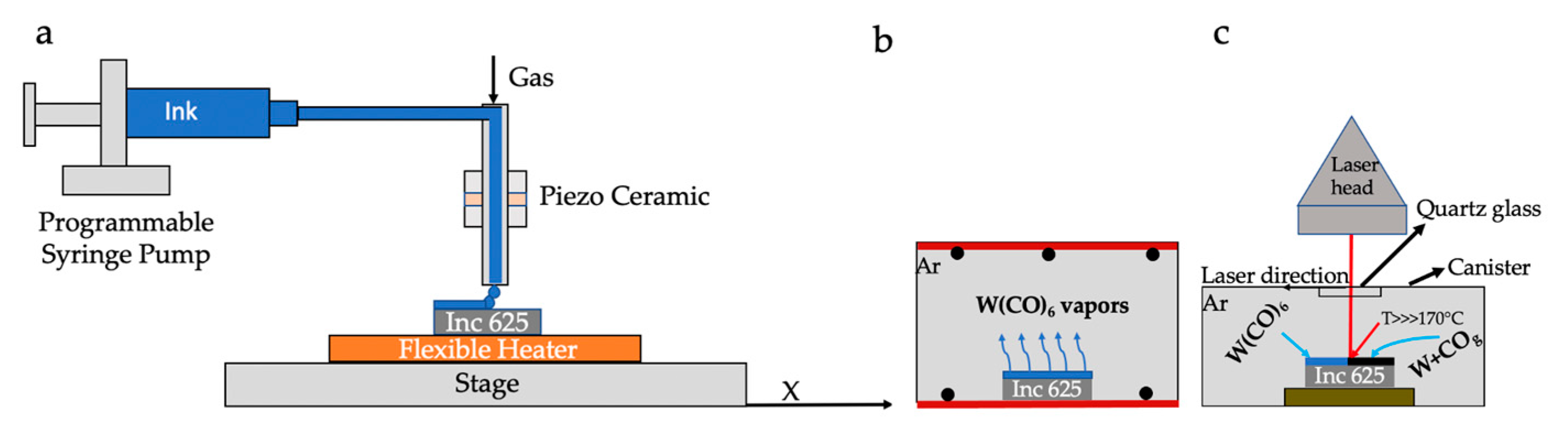
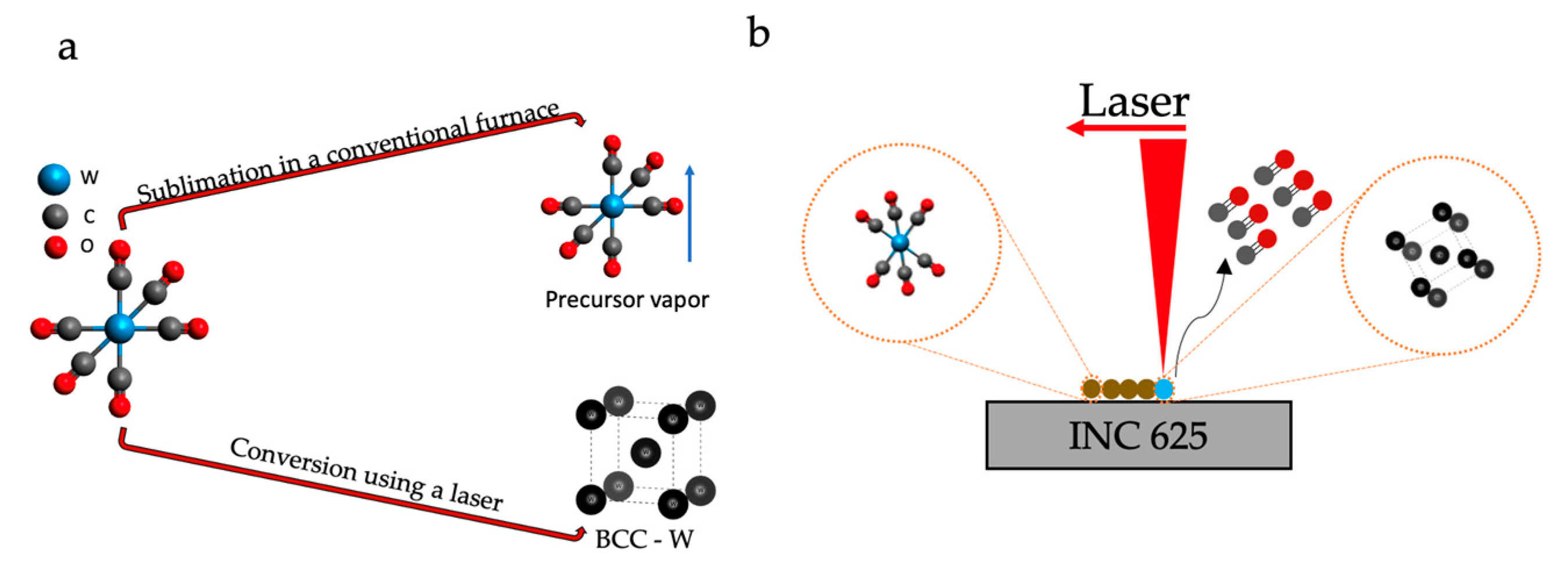
2.2. Deposition of Precursor and Laser-Assisted Conversion

The deposition was carried through a Sonozap ultrasonic atomizer connected with a new era syringe pump system and griffin motion stage to control. The syringe pump was programmed to deliver the same volume each time with a flow rate of 5 mL/h, and the movement of the substrate was controlled in one direction using the stage during the printing and in other directions manually. The substrate was heated to 40 °C using an external heater to remove solvent during the printing.
The printed precursor was then converted using a 1000 W Rofin FL010 laser welder (1080 nm). An inert atmosphere was provided during the laser conversion by placing the precursor inside a vacuum canister that consists of a vacuum flange sealed with an IR-transparent quartz plate and permits the ultra-high purity argon (99.999%). Different laser beam powers (P) of 60, 200, and 400 W at a scan speed of 1000 mm/s were used to study the conversion of the precursor. Laser power of 200 W was used to investigate the effect of atmosphere and precursor amount because no significant change in the reflectance of samples manufactured at 200 W and 400 W was observed. Figure 1a,c show the schematics of the deposition setup and the laser conversion setup, respectively. Table 1 shows the experimental conditions.

2.3. Characterization Methods

Thermogravimetry analysis (TGA, TA instruments Q500) was used to study the effect of heating rate on the precursor. An X-ray diffractometer (XRD, Bruker-D8, Cu-Kα radiation) was used to examine the crystal structure of as-converted and annealed coatings. Scanning electron microscopy (S.E.M., Quanta 600) and transmission electron microscopy (TEM/STEM, FEI Titan 80-200) were used to analyze the nanostructured W coatings morphologies, size, and composition. The focused ion beam lift-out technique (FIB, FEI Helios 650 dual beam) was used to make samples for TEM/STEM analysis. UV-VIS-NIR spectroscopy (JASCO V-670 with an integrated sphere) was used to measure the reflectance of the nanostructured W over the wavelength range of 280 to 2500 nm.

3. Results and Discussion

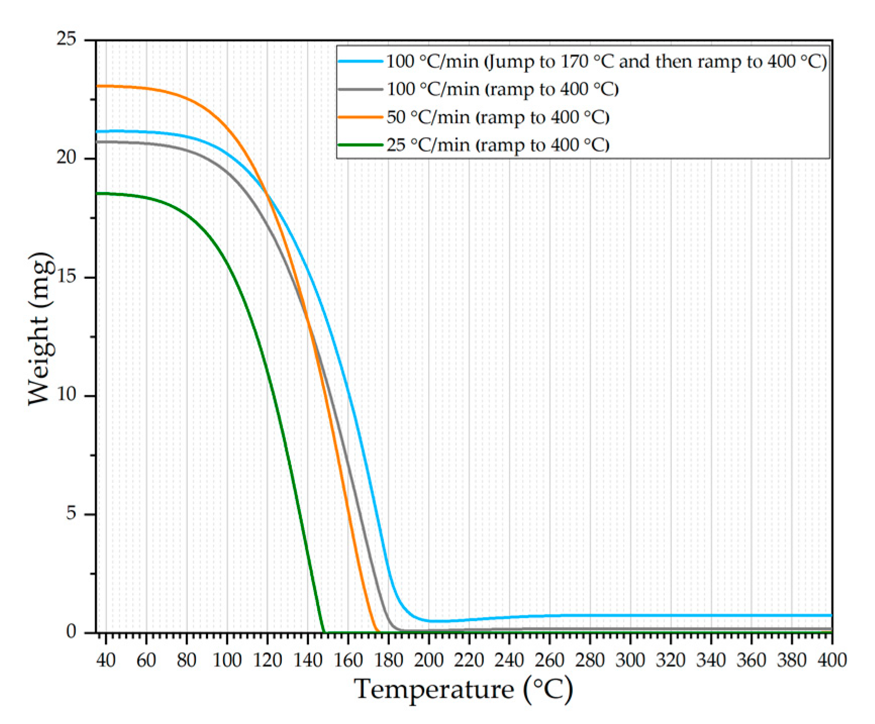
3.1. Thermogravimetric Analysis (TGA)

TGA was used to study the feasibility of a CVD precursor for a solution-processed method since the precursor is highly volatile and has to be converted after deposition on the substrate. In the first three experiments, the temperature was increased from 35 °C to 400 °C at different heating rates of 25 °C/min, 50 °C/min, and 100 °C/min. In the fourth experiment, the temperature was increased from room temperature to 170 °C, which is the onset of decomposition temperature of the precursor. Then, the temperature was further increased to 400 °C using a heating rate of 100 °C/min. Figure 2 shows that the precursors from four different runs started sublimating at temperatures around 65 °C and entirely sublimated when temperatures reached around 150–190 °C.
Additionally, a blue-colored substance was observed on the TGA pan and basket of the fourth run, in which the temperature was ramped up to the decomposition temperature. This color is due to the decomposition of the precursor and the formation of WOX [18]. The oxygen source might be from the regular grade nitrogen used in the experiments. Since heating was carried through a conventional furnace in TGA, information typically obtained from a TGA curve could not be seen. From the TGA curves, the precursor slowly sublimated, starting around 60 °C. Once the temperature was >100 °C, the sublimation rate was rapid. Therefore, the precursor deposited on the substrate baked in a regular furnace sublimed instead of decomposing. If the furnace temperature was >170 °C, they sublimed from the substrate and deposited on the hot walls (Figure 1b). Since the precursor vapor pressure is very high, the decomposition dominated the sublimation if the decomposition temperatures were reached very quickly. This can be achieved using a laser for heating the deposited volatile precursor because laser heating rates are very high [19]. Hence, when the laser is incident on the precursor, decomposition temperature can reach within microseconds locally, forming W before it sublimates (Figure 3a,b).

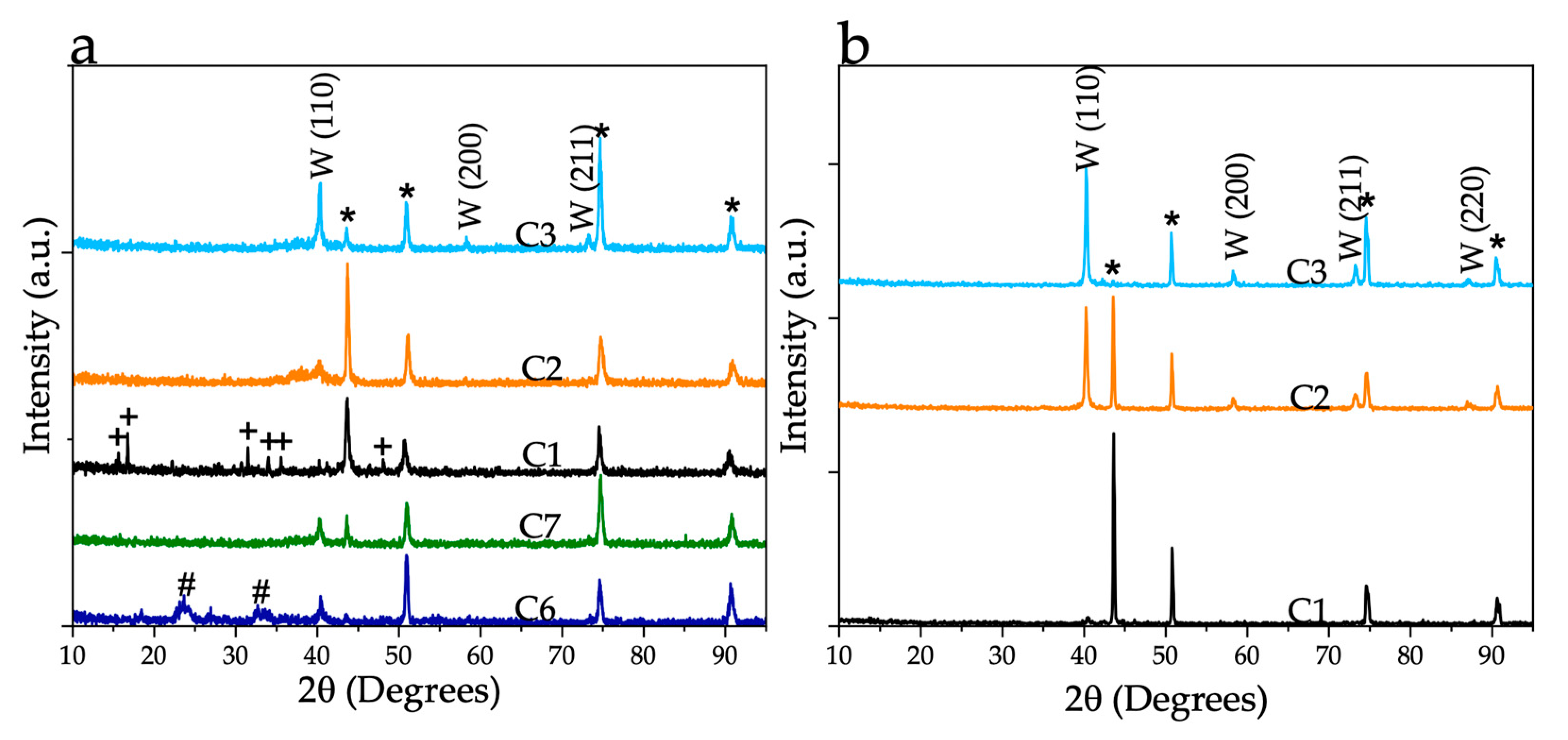
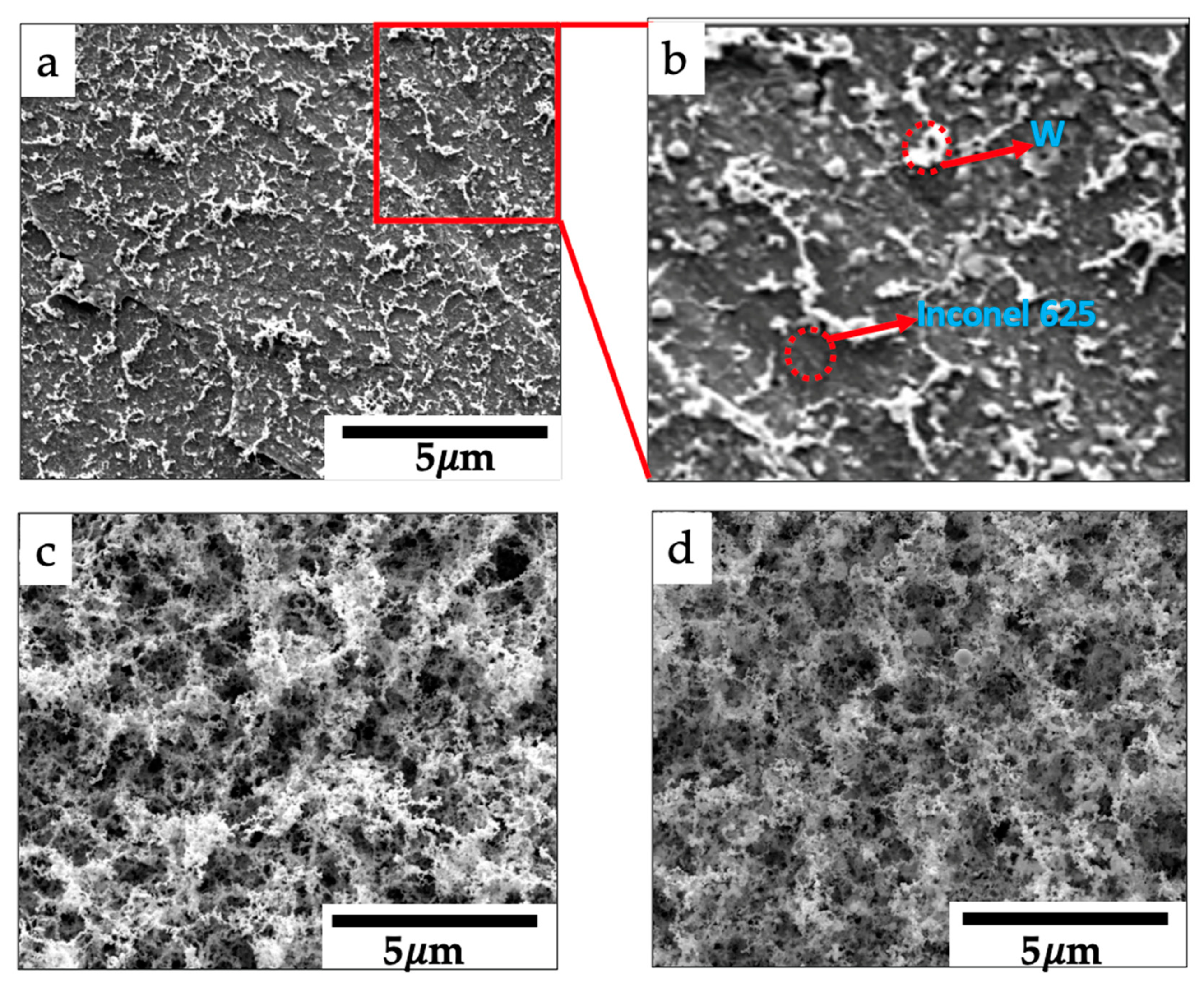
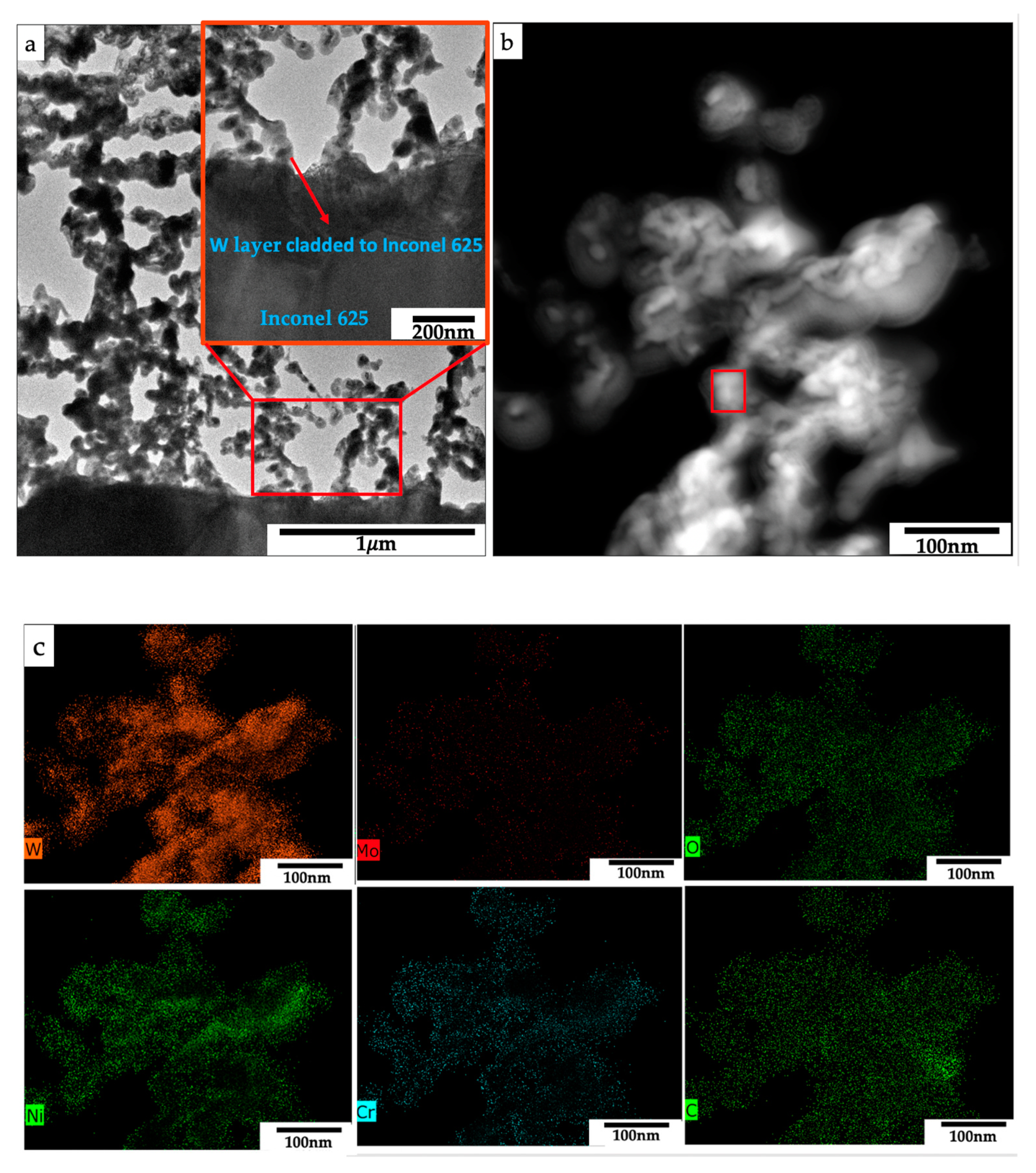
3.2. Crystal Structure, Morphology, and Composition

Figure 4a,b show the XRD patterns of the as-converted precursor using different laser beam powers, different oxygen content in the laser canister, and heat-treated samples at 900 °C for 1 h in the vacuum. As-converted samples show α-W (BCC) peaks (01-089-4900). Based on the XRD data, the presence of precursor peaks (Supplementary Figure S1) indicates that the C1 sample was not fully converted. However, the samples using the higher laser powers show complete conversion. This result suggests that the laser beam power of 60 W was not high enough for the complete conversion of the precursor. In addition, coatings consisting of W/WOX were obtained when the O2 concentration in the canister was maintained at 21 vol%, while no WOX was detected when the O2 content of 1.8 vol% was used. This confirms that hard vacuum (10−6 torr) conditions [1] are not necessary to obtain W metallic coatings, which is beneficial for the scalable production of the materials for industries. The samples C1, C2, and C3 annealed in the vacuum at 900 °C showed an increase in the intensity of W peaks. This is due to an increase in the crystallinity of the coatings. Ni-W intermetallic phases were not detected in XRD. Annealed samples were characterized to determine the morphology and composition of the W nanostructures.
W ( CO ) 6     W + 6   CO ,
2   CO     CO 2 + C
In addition to the above reaction pathways, CO disassociation can occur and form C and O atoms at lower temperatures. The reformation of CO occurs only at higher temperatures. Another reaction pathway is the disproportionation reaction (Boudouard reaction), in which CO converts to CO2 and C at a temperature <700 °C. However, when the temperature is >700 °C, the backward reaction is thermodynamically favorable [20]. In previous work [3], films deposited at temperatures <400 °C contained C and O impurities due to CO disassociation at lower temperatures. When the deposition temperature was >540 °C, fewer impurities were trapped in the films. This is attributed to the less favorable nature of CO disassociation into C and O at higher temperatures. Additional heat treatment of samples at more elevated temperatures further reduced the impurities. This is due to the formation and evolution of CO from C and O impurities in the films at higher temperatures [3]. Using laser heating can reduce the impurities as laser energy produces very high temperatures within microseconds. The CO gas combustion was observed in the canister during a laser scan, which resulted in soot formation on the quartz glass. The soot formation is due to the temperature drop of CO as it leaves the substrate and is combusted into CO2 and elemental C. This observation implies that CO disproportionation occurred rather than disassociation after leaving the substrate.
In previous studies [3], the W films produced by CVD tended to form β-W (A15) at a lower temperature. The SEM and TEM micrographs shown in Figure 5 and Figure 6 show that W nanoparticles are sintered and formed porous nanostructured layer, indicating that temperatures achieved very close to half of the melting point of W (~1700 °C). This result explains why α-W (BCC) is formed rather than the metastable β-W (A15). During the decomposition, CO can also act as a reducer. Thus, no WOx peaks were observed when 1.8 vol% oxygen was used in the canister. The formation of blue WOX and W in sample C6 was due to the O2 deficiency [18].
The SEM micrographs of the heat-treated samples converted at different laser powers are shown in Figure 5. The film showed a rough and porous network structure. Furthermore, the converted W with the laser power of 60 W had sparser W nanostructures on the substrate (Figure 5a,b) than the samples, C2 and C3, processed at higher laser powers (Figure 5c,d). This was also visually observed after the experiment. After taking it out from the laser canister, the coating on the C1 had a mixture of precursor (white color) and tungsten (black). This precursor was sublimated during the heat treatment because of its very high vapor pressure, and as a result, sparser nanostructures were seen on the micrograph (Figure 5a). This reveals that it was a partial conversion and incomplete reaction; the temperature of the substrate for sample C1 was much lower than those of the other two samples as a result of different laser parameters.
Further, TEM/STEM was used to analyze the heat-treated sample C2. The sample was prepared by FIB lift-out. C and Pt layers were deposited over the film (for protection). Figure 6a shows the cross-sectional micrograph of the converted W cladded onto the Inconel 625 substrate. Nanoparticles were generated with voids and sintered to form a continuous network of nanostructures. The converted W nanostructures were not melted but partially sintered during the laser cladding, supported by the structure with a high void fraction as shown in TEM (Figure 6a) due to the high melting temperature.
Furthermore, STEM-EDS elemental maps were obtained to investigate the distribution of the elements within the network structures. Based on Figure 6b,c and Table 2, the Inconel 625 elements were also homogeneously found from the W nanostructures. This indicates that the generated W particles likely circulated in the melt pool of Inconel 625 as a result of Marangoni flow [21]. During Marangoni flow, the melt wetted the W networks, and then the W nanostructure rose to the top surface. This is because of the lower density of the W nanoparticles, due to its porous nanostructured network, compared with the melt pool. In addition, 2.9% of W was observed in the Inconel 625 matrix. This might be due to the small amount of W particles fully melted and remained in the matrix because of their high density (Supplementary Figure S2 and Table S1). Carbon percentage may not be solely from our sample as the e-beam carbon layer and ion beam carbon layers were deposited before the Pt layer to protect the sample.

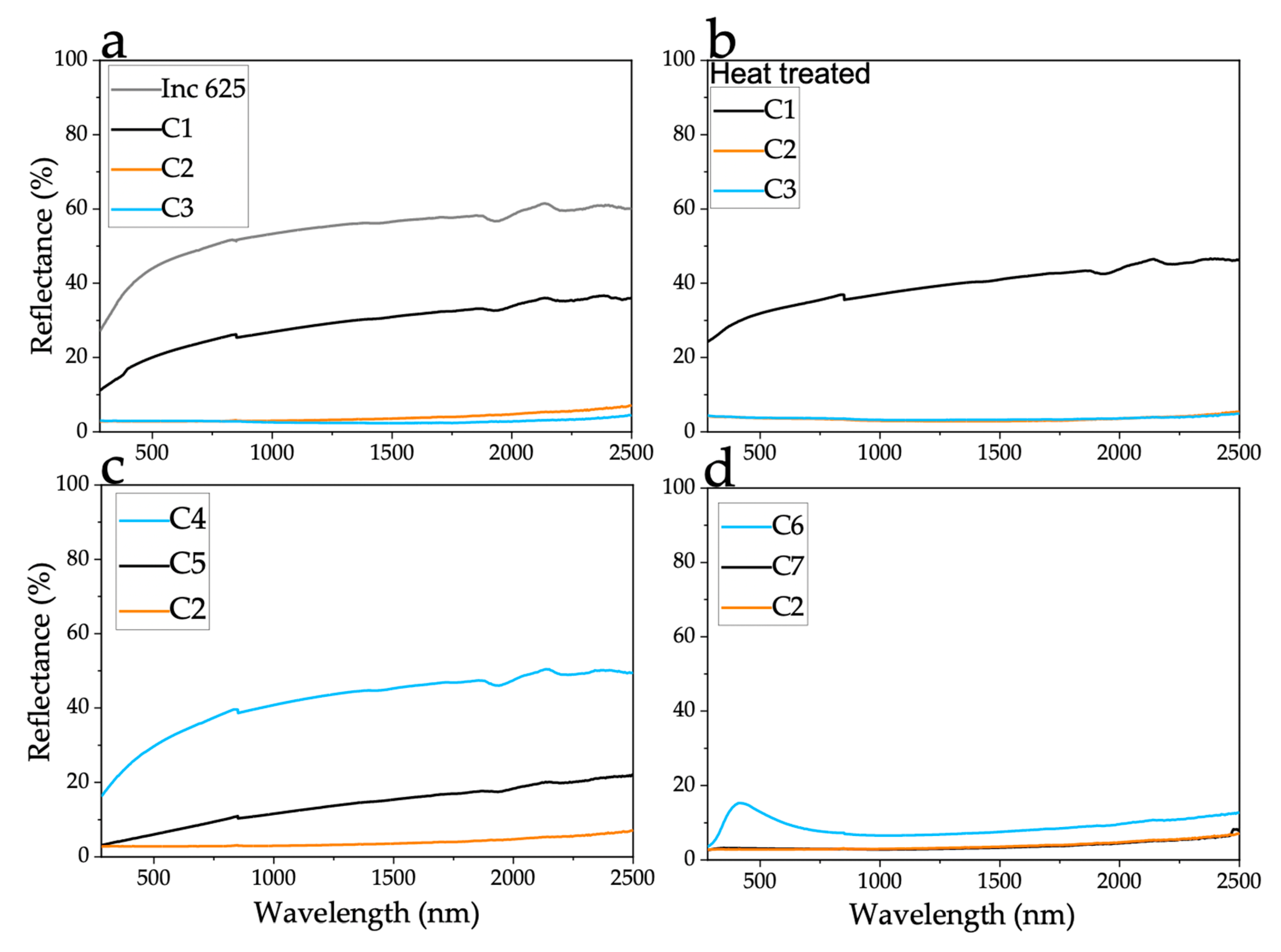
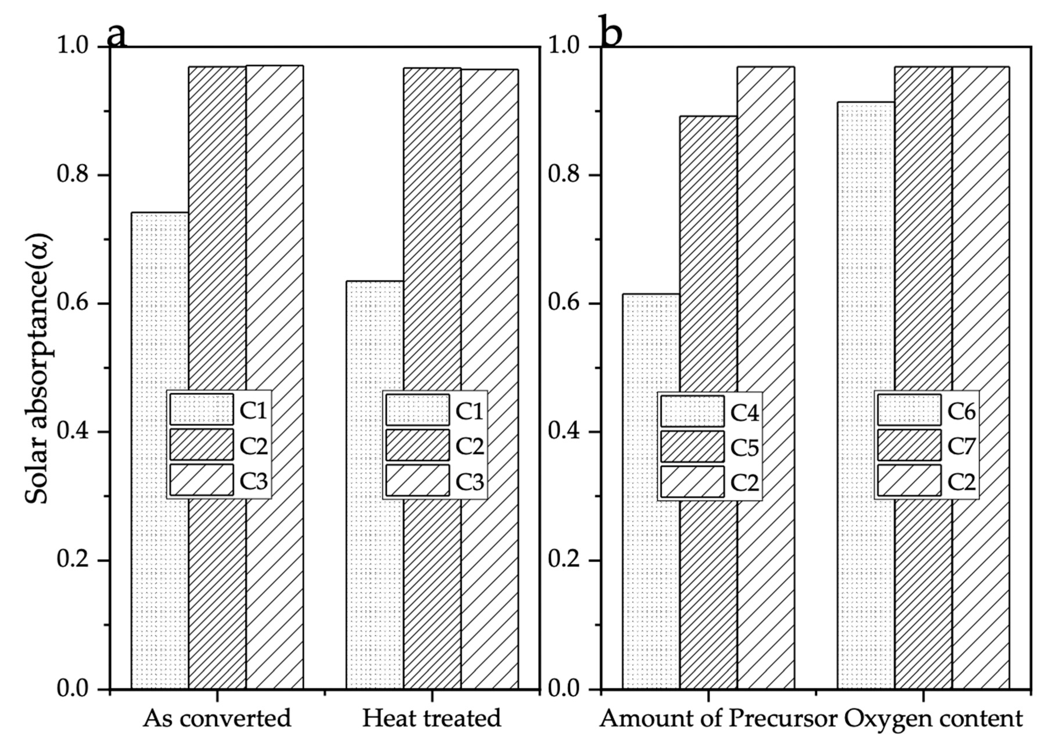
3.3. UV-VIS-NIR Reflectance and Solar Absorbance

The UV-VIS-NIR reflectance of the samples was measured over the wavelength of 280–2500 nm. The solar absorptance was calculated by the weighted fraction of solar absorption of the material and incident solar radiation. The solar absorption was calculated for all the samples using the ASTM G173-03 reference spectra [22]. Figure 7 and Figure 8 show the reflectance of the samples and solar absorptance value of samples at different experimental conditions, respectively. The reflectance of samples was reduced compared to bare Inconel 625 substrate. This can be attributed to the sub-wavelength structures of W formed on the Inconel 625 substrate surface, creating a surface plasmon absorption, thereby enhancing the solar absorptance [9]. The solar absorptance of bare Inconel 625 substrate was 48.8%, and C2 and C3 were almost the same at about 96.9% and 97.2% before and after heat treatment at 900 °C in vacuum for 1 h, respectively. The solar absorptance of as-converted sample C1 was 74.2% and decreased to 63.5% after heat treatment. The coating on the as-converted C1 sample was a mixture of W and unconverted precursor. This unconverted precursor was sublimated after heat treatment resulting in coatings with less area covered by the W layer. Consequently, solar absorptance is the average of both the coating and substrate.
α = 280   nm 2500   nm ( 1 - R ( λ ) )   I ( λ )   d λ 280   nm 2500   nm I ( λ )   d λ ,
With the different amounts of precursor ink, the thickness of W coating varies, and with 0.1 ml ink, the coating was not uniform relative to the 1 mL ink. The absorptance of sample C4 was 61.5%, and that of C5 was 89.2%. Further experiments are needed to optimize the thickness to better make the coatings cladded to the Inconel surface (only C4 has better adhesion, and the remaining can be washed away) and improve solar absorptance. The effect of O2 concentration was also studied on the conversion and solar absorptance. At the atmospheric O2 content (21 vol%), the coating contained a mixture W/WOx, and the solar absorptance dropped to 91.4%. However, with 1.8 vol% O2, the solar absorptance was almost the same as the samples converted in an inert atmosphere. This experiment shows that high solar absorptance coatings could be manufactured at ambient pressures, which is advantageous to large-scale production.
The IR emissivity of samples was not measured in this work since the solar absorptance is more important. The emissivity effect was not significant at practical receiver temperatures but could become significant at very high temperatures [23]. However, W is an inherent IR reflector, and previous studies [4] show that the emissivity of SS substrates decreased with increasing W thickness. The deposited coatings (sample C2) in this work were relatively thick (about 5–6 µm, Supplementary Figure S3), and by controlling the amount of precursor and layer by layer deposition and conversion, the adhesion and thickness can be further optimized for better solar absorptance and low IR emissivity.

4. Conclusions

Nanostructured W coatings were manufactured by laser conversion of tungsten hexacarbonyl on Inconel 625 substrates under an argon environment at ambient pressure. The results show that a network of black W nanostructures was obtained. STEM/EDS revealed the presence of Inconel 625 elements on W structures. XRD analysis revealed the formation of α-W at higher laser powers and W/WOx peaks with an oxygen concentration of 21 vol% and only W peaks when the oxygen concentration was 1.8 vol% and 0.5 ppm was used in the laser canister. About 97% solar absorptance was achieved with W coatings of 5–6 µm and varied with the amount of precursor deposited, uniformity of the layer, and oxygen concentration in the canister during laser conversion. Future work is needed to improve the process by uniformly depositing precursor, controlling thickness per layer, and further optimizing laser parameters to get better cladding to the substrate. Functional alloys with tailored solar absorption can be additively manufactured by integrating precursor ink chemistry with a hybrid metal additive manufacturing process. The main advantage will be to manufacture such structures in one single step without the need for post-processing. Additionally, by voxel-controlling the amount of precursor, functionally graded structures can be manufactured with specific target properties.

Supplementary Materials

The following are available online at https://www.mdpi.com/article/10.3390/nano11092304/s1, Figure S1: XRD of tungsten hexacarbonyl precursor, Figure S2: STEM/EDS of a cross-section, Table S1: Elemental composition of Inconel 625 just below the interface, Figure S3: Cross-section of the tungsten coating.

Author Contributions

V.V.K.D. and C.-H.C. conceived and designed the experiments; V.V.K.D. performed the experiments, analyzed the data, and prepared the draft; T.T.C. performed TGA experiments and reviewed the manuscript; K.L. and V.V.K.D. performed the laser canister experiments; K.L. and S.M. reviewed and edited the manuscript; B.K.P., S.P. and C.-H.C., acquired funding and reviewed and edited the final manuscript. All authors have read and agreed to the published version of the manuscript.

Funding

Department of Energy (DOE) (DE-EE0007888-10-4) Advanced Manufacturing Office (AMO) and the Rapid Advancement in Process Intensification Deployment (RAPID) Institute. Part of this work was conducted at the Oregon Process Innovation Center (OPIC), a National Nanotechnology Coordinated Infrastructure site at the Oregon State University (OSU), which is supported in part by NSF (grant ECC-1542101) and OSU. The authors would like to acknowledge the funding of equipment provided by the Murdock Charitable Trust (contract #2016231); NSF funds the TEM via the Major Research Instrumentation (MRI.) Program under Grant No. 1040588. S.P. would like to acknowledge the grant received from the National Science Foundation (NSF) Advanced Manufacturing Program (award number: 1856412).

Institutional Review Board Statement

Not applicable.

Informed Consent Statement

Not applicable.

Data Availability Statement

Data is presented within the article.

Acknowledgments

Peter Eschbach for FIB and TEM. The authors also thank Oregon State University electron microscopy center, thermal characterization facility in Skip Rochefort’s lab, and the ATAMI facility staff and director.

Conflicts of Interest

The authors declare no conflict of interest.

References

  1. Gao, X.H.; Guo, Z.M.; Geng, Q.F.; Ma, P.J.; Liu, G. Enhanced absorptance of surface-textured tungsten thin film for solar absorber. Surf. Eng. 2016, 32, 840–845. [Google Scholar] [CrossRef]
  2. Zhang, H.; Feng, P.; Akhtar, F. Aluminium matrix tungsten aluminide and tungsten reinforced composites by solid-state diffusion mechanism. Sci. Rep. 2017, 7, 1–8. [Google Scholar] [CrossRef] [PubMed]
  3. Lai, K.K.; Lamb, H.H. Tungsten chemical vapor deposition using tungsten hexacarbonyl: Microstructure of as-deposited and annealed films. Thin Solid Films 2000, 370, 114–121. [Google Scholar] [CrossRef]
  4. Sibin, K.P.; John, S.; Barshilia, H.C. Control of thermal emittance of stainless steel using sputtered tungsten thin films for solar thermal power applications. Sol. Energy Mater. Sol. Cells 2015, 133, 1–7. [Google Scholar] [CrossRef]
  5. Wang, W.; Wen, H.; Ling, S.; Li, Z.; Su, J.; Wang, C. Self-doped W-WO: X nanocermet multilayer films fabricated by single tungsten target reactive sputtering for selective solar absorption. J. Mater. Chem. A 2018, 6, 15690–15700. [Google Scholar] [CrossRef]
  6. Han, X.; He, K.; He, Z.; Zhang, Z. Tungsten-based highly selective solar absorber using simple nanodisk array. Opt. Express 2017, 25, A1072. [Google Scholar] [CrossRef] [PubMed]
  7. Liang, Q.; Yin, Q.; Chen, L.; Wang, Z.; Chen, X. Perfect spectrally selective solar absorber with dielectric filled fishnet tungsten grating for solar energy harvesting. Sol. Energy Mater. Sol. Cells 2020, 215, 110664. [Google Scholar] [CrossRef]
  8. Koya, A.N.; Zhu, X.; Ohannesian, N.; Yanik, A.A.; Alabastri, A.; Proietti Zaccaria, R.; Krahne, R.; Shih, W.C.; Garoli, D. Nanoporous metals: From plasmonic properties to applications in enhanced spectroscopy and photocatalysis. ACS Nano 2021, 15, 6038–6060. [Google Scholar] [CrossRef] [PubMed]
  9. Shah, A.A.; Gupta, M.C. Spectral selective surfaces for concentrated solar power receivers by laser sintering of tungsten micro and nano particles. Sol. Energy Mater. Sol. Cells 2013, 117, 489–493. [Google Scholar] [CrossRef]
  10. Gesheva, K.A.; Gogova, D.S.; Stoyanov, G. Black tungsten selective optical coatings for photothermal solar energy conversion. J. Phys. III 1992, 2, 1453–1459. [Google Scholar] [CrossRef]
  11. Salama, E.; Eissa, M.M.; Tageldin, A.S. Distinct properties of tungsten austenitic stainless alloy as a potential nuclear engineering material. Nucl. Eng. Technol. 2019, 51, 784–791. [Google Scholar] [CrossRef]
  12. Paul, B.K.; Lee, K.; He, Y.; Ghayoor, M.; Chang, C.H.; Pasebani, S. Oxide dispersion strengthened 304 L stainless steel produced by ink jetting and laser powder bed fusion. CIRP Ann. 2020, 69, 193–196. [Google Scholar] [CrossRef]
  13. Raghu, T.; Sundaresan, R.; Ramakrishnan, P.; Rama Mohan, T.R. Synthesis of nanocrystalline copper-tungsten alloys by mechanical alloying. Mater. Sci. Eng. A 2001, 304, 438–441. [Google Scholar] [CrossRef]
  14. Guo, Y.; Guo, H.; Gao, B.; Wang, X.; Hu, Y.; Shi, Z. Rapid consolidation of ultrafine grained W-30 wt.% Cu composites by field assisted sintering from the sol-gel prepared nanopowders. J. Alloys Compd. 2017, 724, 155–162. [Google Scholar] [CrossRef]
  15. Okamoto, H.; Akira, I. Tungsten metal film formed by spin-coating amorphous peroxopolytungstic acid. Appl. Phys. Lett. 1989, 55, 1923–1925. [Google Scholar]
  16. Wilkinson, N.J.; Smith, M.A.A.; Kay, R.W.; Harris, R.A. A review of aerosol jet printing—A non-traditional hybrid process for micro-manufacturing. Int. J. Adv. Manuf. Technol. 2019. [Google Scholar] [CrossRef] [Green Version]
  17. Tonneau, D.; Auvert, G.; Pauleau, Y. Laser-induced decomposition of metal carbonyls for chemical vapor deposition of microstructures. J. Phys. Colloq. 1989, 50, C5-647–C5-656. [Google Scholar] [CrossRef] [Green Version]
  18. Gogova, D.; Gesheva, K.; Kakanakova-Georgieva, A.; Surtchev, M. Investigation of the structure of tungsten oxide films obtained by chemical vapor deposition. Eur. Phys. J. Appl. Phys. 2000, 167–174. [Google Scholar] [CrossRef]
  19. Sowdari, D.; Majumdar, P. Finite element analysis of laser irradiated metal heating and melting processes. Opt. Laser Technol. 2010, 42, 855–865. [Google Scholar] [CrossRef]
  20. Hunt, J.; Ferrari, A.; Lita, A.; Crosswhite, M.; Ashley, B.; Stiegman, A.E. Microwave-specific enhancement of the carbon-carbon dioxide (boudouard) reaction. J. Phys. Chem. C 2013, 117, 26871–26880. [Google Scholar] [CrossRef]
  21. Yuan, P.; Gu, D.; Dai, D. Particulate migration behavior and its mechanism during selective laser melting of TiC reinforced Al matrix nanocomposites. Mater. Des. 2015, 82, 46–55. [Google Scholar] [CrossRef]
  22. ASTM International. G173-03(2012) Standard Tables for Reference Solar Spectral Irradiances: Direct Normal and Hemispherical on 37° Tilted Surface; ASTM International: West Conshohocken, PA, USA, 2012. [Google Scholar]
  23. Ho, C.K. Advances in central receivers for concentrating solar applications. Sol. Energy 2017, 152, 38–56. [Google Scholar] [CrossRef]
Figure 1. Schematics of experimental setup (a) precursor deposition setup; (b) precursor deposited substrate placed in a conventional furnace; (c) laser canister setup used in this work.
Nanomaterials 11 02304 g001
Figure 2. TGA curves of tungsten hexacarbonyl at different heating rates in nitrogen.
Nanomaterials 11 02304 g002
Figure 3. Chemistry of aerosol deposited precursor on the substrate. (a) transformation of precursor using different heating methods; (b) laser-induced decomposition of tungsten hexacarbonyl precursor.
Nanomaterials 11 02304 g003
Figure 4. XRD of the samples converted at different energy densities: (a) as-converted samples and (b) heat-treated in vacuum at 900 °C for 1 h (* denotes Inconel 625 substrate; # denotes WOx peaks; + denotes W(CO)6 peaks).
Nanomaterials 11 02304 g004
Figure 5. Surface morphology of samples converted at different laser beam powers and heat-treated at 900 °C using SEM: (a) C1, (b) zoomed in micrograph of C1(highlighted area), (c) C2, and (d) C3.
Nanomaterials 11 02304 g005
Figure 6. (a) TEM micrographs of Sample C2 showing sintered nanostructure and the cladded W nanostructures to the Inconel 625 substrate; (b) STEM micrograph of W network at higher magnification; (c) STEM-EDS elemental mapping of sample C2.
Nanomaterials 11 02304 g006
Figure 7. UV-VIS-NIR reflectance of samples. (a) as-converted samples at different laser beam power, (b) heat-treated samples at 900 °C for 1 h, (c) as-converted samples with different amounts of precursor deposited, (d) as-converted precursor at different O2 concentrations.
Nanomaterials 11 02304 g007
Figure 8. Solar absorptance of coated samples manufactured at different experimental conditions. (a) as-converted and heat-treated samples, (b) as-converted samples with different precursor amounts and at different O2 concentrations.
Nanomaterials 11 02304 g008
Table 1. Manufacturing conditions.
SampleLaser Power (W)Scan Speed
(mm/s)
AtmosphereAmount of Precursor Ink Deposited (mL)
C1601000Ar1.0
C22001000Ar1.0
C34001000Ar1.0
C42001000Ar0.1
C52001000Ar0.35
C6200100021 vol% O21.0
C720010001.8 vol% O2/Ar1.0
Table 2. Elemental composition of the W nanostructures (highlighted area in Figure 5b).
ElementsWNiCrMoFeTaNbSiOCMnAlCoTiPt
Mass%52.27.333.082.181.767.952.282.964.306.661.161.451.450.634.55
At%35.210.114.922.312.555.512.576.129.679.021.704.062.041.093.08
Publisher’s Note: MDPI stays neutral with regard to jurisdictional claims in published maps and institutional affiliations.

