
Fundamental Aspects and Comprehensive Review on Physical Properties of Chemically Grown Tin-Based Binary Sulfides

 ,
, 
Abstract
1. Introduction
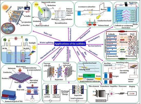
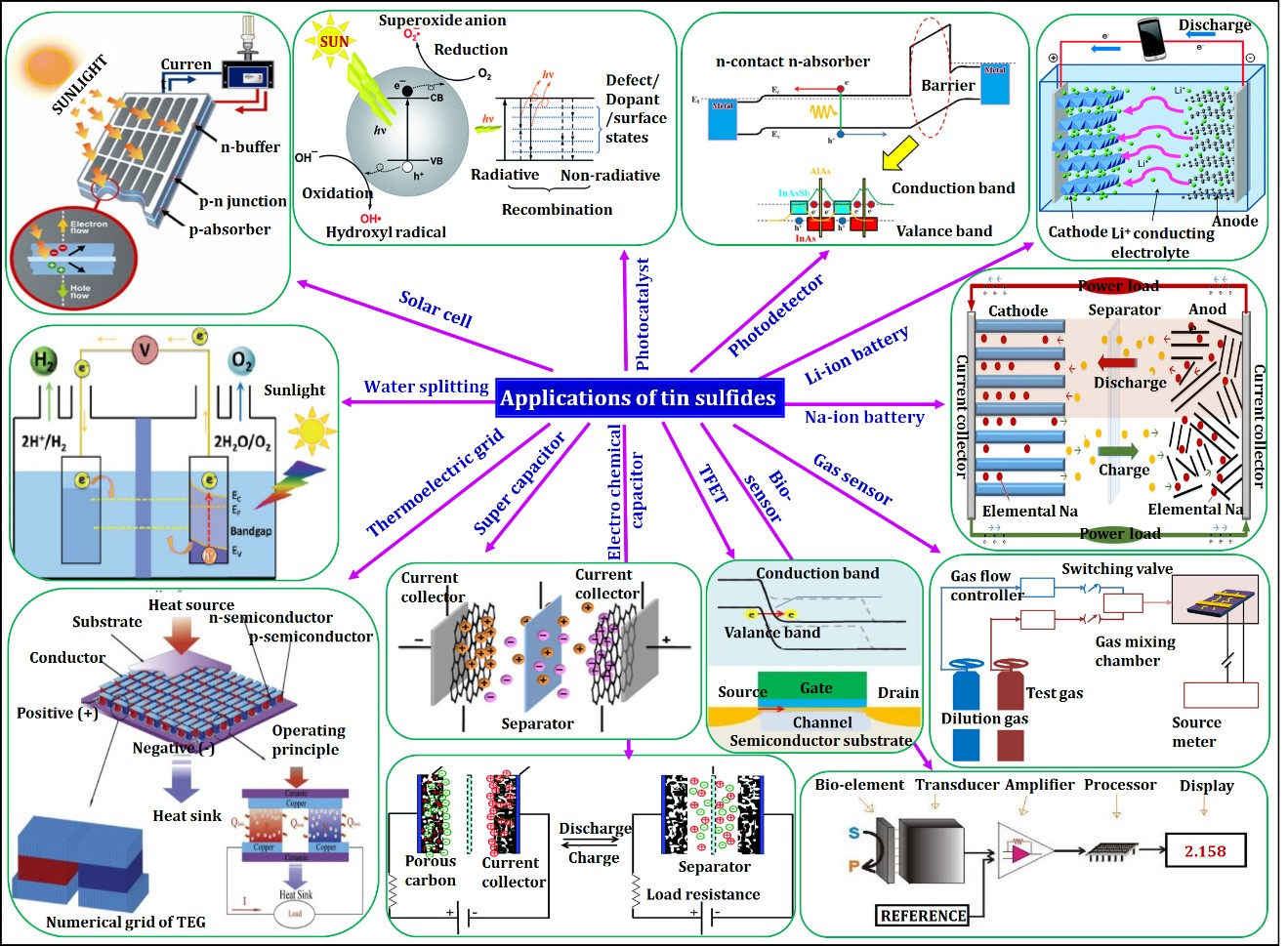
2. Physical Properties of o-SnS, c-SnS, SnS2, and Sn2S3
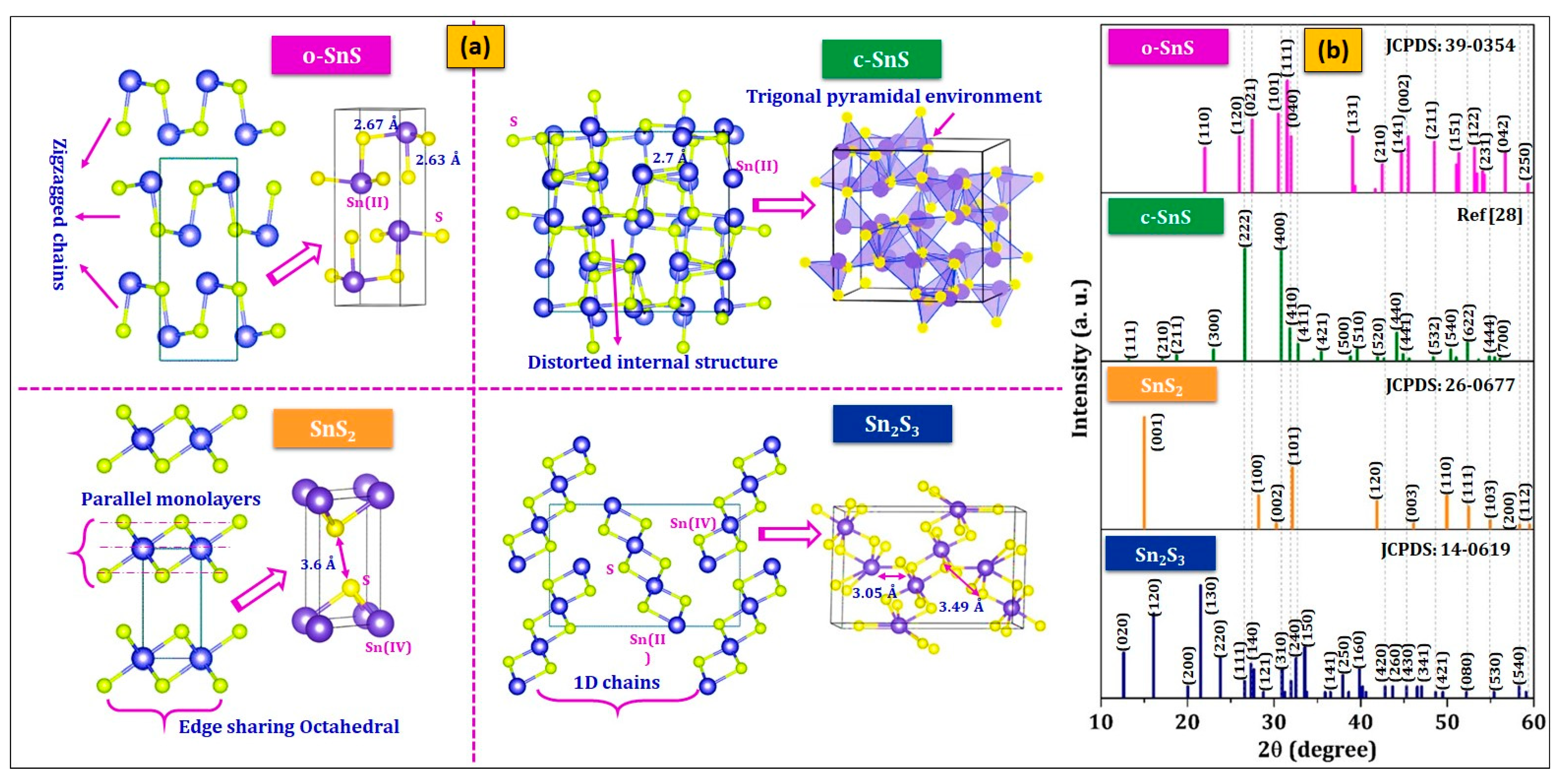
2.1. Crystal Structure and Structural Characteristics
2.2. Electronic Band Structure and Optical Characteristics
2.3. Conduction Type and Electrical Characteristics
3. Influence of Deposition Parameters on SnxSy Thin Film Growth and Properties
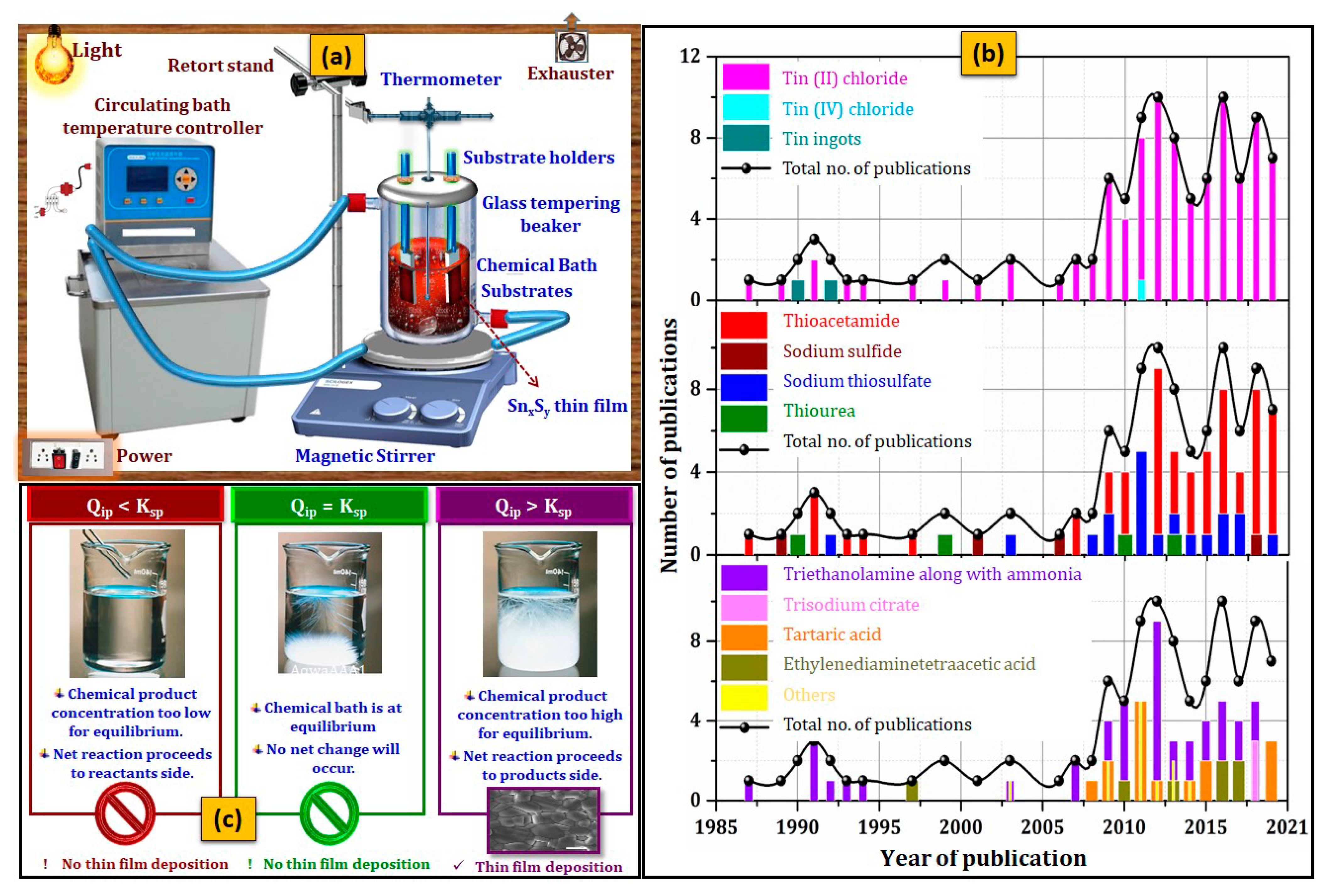
3.1. Overview of CBD Process of SnxSy Thin Films
3.2. Sn and S Precursors and Their Concentration Effect
3.3. Complexing Agents and Their Concentration Effect
3.4. Solution pH Effect
3.5. Solution Temperature (Tb) Effect
3.6. Deposition Time Effect
3.7. Other Parameters
3.7.1. Substrate Nature and Its Cleaning Process Effect
3.7.2. Stirring Speed and Humidity Effect
3.8. Summary
4. Conclusions
Author Contributions
Funding
Data Availability Statement
Conflicts of Interest
Abbreviations
| Abbreviation | Chemical Name |
| A | Ammonia |
| AA | Acetic acid |
| AC | Ammonium citrate |
| ACE | Acetone |
| AF | Ammonium fluoride |
| AH | Ammonium hydroxide |
| ALD | Atomic layer deposition |
| AS | Ammonium sulfide |
| BT | Baking temperature |
| CA | Citric acid |
| CALPHAD | CALculation of PHAse diagram |
| CBD | Chemical bath deposition |
| CBM | Conduction band minimum |
| CBO | Conduction band offset |
| CSS | Close space sublimation |
| CUB | Cubic |
| DDT | Dodecanethiol |
| DIW | Deionized water |
| DW | Distilled water |
| EDS | Energy-dispersive X-ray spectroscopy |
| EDTA | Ethylenediaminetetraacetic acid |
| EL | Electrolyte |
| FF | Fill factor |
| G | Glass |
| GA | Glacial acetic acid |
| GIXRD | Grazing incidence X-ray diffraction |
| HCL | Hydrochloric acid |
| HEX | Hexagonal |
| HH | Hydrazine hydrate |
| HWVD | Hot wall vapor deposition |
| ITO | Indium tin oxide |
| JCPDS | Joint committee on powder diffraction standards |
| Li | Lithium |
| MeOH | Methanol |
| Mo | Molybdenum |
| Na | Sodium |
| Na2EDTA | Disodium ethylenediaminetetraacetate |
| NTA | Nitriloacetic acid |
| ODE | Ooctadecene |
| OLA | Oleylamine |
| ORT | Orthorhombic |
| PG | Propylene glycol |
| PL | Photoluminescence |
| QE | Quantum efficiency |
| RS | Rock salt |
| SAED | Selected area electron diffraction |
| SCR | Space charge region |
| SDS | Sodium sulfide |
| Si | Silicon |
| SILAR | Successive ionic layer adsorption and reaction |
| SIMS | Secondary ion mass spectrometry |
| SS | Stainless steel |
| SnS | Tin monosulfide |
| SnS2 | Tin disulfide |
| Sn2S3 | Tin sesquisulfide |
| ST | Sodium thiosulfate |
| TA | Thioacetamide |
| T(II)C | Tin (II) chloride dehydrate |
| TC(IV) | Tin(IV) chloride pentahydrate |
| TEA | Triethanolamine |
| TEM | Transmission electron microscopy |
| Ti | Titanium |
| TO | Tin oxide |
| TOP | Trioctylphosphine oxide |
| Tr | Room temperature |
| TSC | Trisodium citrate |
| TTA | Tartaric acid |
| TU | Thiourea |
| UAED | Ultrasound-assisted electrodeposition |
| VBM | Valence band maximum |
| XRD | X-ray diffraction |
| ZB | Zinc blended |
References
- De Elisa, R. Cadmium telluride solar cells: Selenium diffusion unveiled. Nat. Energy 2016, 1, 16143–16146. [Google Scholar]
- Solar Frontier Achieves World Record Thin-Film Solar Cell Efficiency of 23.35%. Available online: http://www.solar-frontier.com/eng/news/2019/0117_press.html (accessed on 14 July 2021).
- Chen, X.; Hou, Y.; Zhang, B.; Yang, X.H.; Yang, H.G. Low-cost SnSx counter electrodes for dye-sensitized solar cells. Chem. Commun. 2013, 49, 5793–5795. [Google Scholar] [CrossRef] [PubMed]
- PV Division | Business Information | KITAGAWA SEIKI Co., Ltd. Available online: http://www.kitagawaseiki.co.jp/en/jigyo_pv.html (accessed on 14 July 2021).
- Ge, J.; Zhang, Y.; Heo, Y.-J.; Park, S.-J. Advanced Design and Synthesis of Composite Photocatalysts for the Remediation of Wastewater: A Review. Catalysts 2019, 9, 122. [Google Scholar] [CrossRef]
- Liao, C.-H.; Huang, C.-W.; Wu, J.C.S. Hydrogen Production from Semiconductor-based Photocatalysis via Water Splitting. Catalysts 2012, 2, 490–516. [Google Scholar] [CrossRef]
- Zhao, Y.; Yang, Q.; Chang, Y.; Pang, W.; Zhang, H.; Duan, X. Novel Gas Sensor Arrays Based on High-Q SAM-Modified Piezotransduced Single-Crystal Silicon Bulk Acoustic Resonators. Sensors 2017, 17, 1507. [Google Scholar] [CrossRef]
- Campaña, A.; Florez, S.; Noguera, M.; Fuentes, O.; Ruiz Puentes, P.; Cruz, J.; Osma, J. Enzyme-Based Electrochemical Biosensors for Microfluidic Platforms to Detect Pharmaceutical Residues in Wastewater. Biosensors 2019, 9, 41. [Google Scholar] [CrossRef] [PubMed]
- Lee, S.-H.; Park, J.-U.; Kim, G.; Jee, D.-W.; Kim, J.H.; Kim, S. Rigorous Study on Hump Phenomena in Surrounding Channel Nanowire (SCNW) Tunnel Field-Effect Transistor (TFET). Appl. Sci. 2020, 10, 3596. [Google Scholar] [CrossRef]
- Mohammed, M.; Chun, D.-M. Electrochemical Performance of Few-Layer Graphene Nano-Flake Supercapacitors Prepared by the Vacuum Kinetic Spray Method. Coatings 2018, 8, 302. [Google Scholar] [CrossRef]
- Wang, Y.; Mao, Y.; Ji, Q.; Yang, M.; Yang, Z.; Lin, H. Electrostatic Discharge Characteristics of SiGe Source/Drain PNN Tunnel FET. Electronics 2021, 10, 454. [Google Scholar] [CrossRef]
- Li, S.; Lam, K.H.; Cheng, K.W.E. The Thermoelectric Analysis of Different Heat Flux Conduction Materials for Power Generation Board. Energies 2017, 10, 1781. [Google Scholar] [CrossRef]
- Kumar, S.G.; Rao, K.S.R.K. Physics and chemistry of CdTe/CdS thin film heterojunction photovoltaic devices: Fundamental and critical aspects. Energy Environ. Sci. 2014, 7, 45–102. [Google Scholar] [CrossRef]
- Alzoubi, T.; Moustafa, M. Numerical optimization of absorber and CdS buffer layers in CIGS solar cells using SCAPS. Int. J. Smart Grid Clean Energy 2019, 8, 291–298. [Google Scholar] [CrossRef]
- Bag, S.; Gunawan, O.; Gokmen, T.; Zhu, Y.; Todorov, T.K.; Mitzi, D.B. Low band gap liquid-processed CZTSe solar cell with 10.1% efficiency. Energy Environ. Sci. 2012, 5, 7060–7065. [Google Scholar] [CrossRef]
- Jiang, F.; Shen, H.; Gao, C.; Liu, B.; Lin, L.; Shen, Z. Preparation and properties of SnS film grown by two-stage process. Appl. Surf. Sci. 2011, 257, 4901–4905. [Google Scholar] [CrossRef]
- Sreedevi, G.; Vasudeva Reddy, M.; Park, C.; Jeon, C.W.; Ramakrishna Reddy, K.T. Comprehensive optical studies on SnS layers synthesized by chemical bath deposition. Opt. Mater. 2015, 42, 468–475. [Google Scholar] [CrossRef]
- Koteeswara Reddy, N.; Ramakrishna Reddy, K.T. Preparation and characterisation of sprayed tin sulphide films grown at different precursor concentrations. Mater. Chem. Phys. 2007, 102, 13–18. [Google Scholar] [CrossRef]
- Jiang, F.; Shen, H.; Wang, W.; Zhang, L. Preparation of SnS film by sulfurization and SnS/a-Si heterojunction solar cells. J. Electrochem. Soc. 2012, 159, H235. [Google Scholar] [CrossRef]
- Devika, M.; Koteeswara Reddy, N.; Venkatramana Reddy, S.; Ramesh, K.; Gunasekhar, K.R. Influence of rapid thermal annealing (RTA) on the structural and electrical properties of SnS films. J. Mater. Sci. Mater. Electron. 2009, 20, 1129–1134. [Google Scholar] [CrossRef]
- Noguchi, H.; Setiyadi, A.; Tanamura, H.; Nagatomo, T.; Omoto, O. Characterization of vacuum-evaporated tin sulfide film for solar cell materials. Sol. Energy Mater. Sol. Cells 1994, 35, 325–331. [Google Scholar] [CrossRef]
- Ogah, O.E.; Zoppi, G.; Forbes, I.; Miles, R.W. Thin films of tin sulphide for use in thin film solar cell devices. Thin Solid Films 2009, 517, 2485–2488. [Google Scholar] [CrossRef]
- Ragina, A.J.; Murali, K.V.; Preetha, K.C.; Deepa, K.; Remadevi, T.L. A Study of optical parameters of tin sulphide thin films using the swanepoel method. In AIP Conference Proceedings; American Institute of Physics: College Park, MD, USA, 2011; Volume 1391, pp. 752–754. [Google Scholar]
- Mahdi, M.S.; Ibrahim, K.; Hmood, A.; Ahmed, N.M.; Mustafa, F.I.; Azzez, S.A. High performance near infrared photodetector based on cubic crystal structure SnS thin film on a glass substrate. Mater. Lett. 2017, 200, 10–13. [Google Scholar] [CrossRef]
- Nair, P.K.; Garcia-Angelmo, A.R.; Nair, M.T.S. Cubic and orthorhombic SnS thin-film absorbers for tin sulfide solar cells. Phys. Status Solidi Appl. Mater. Sci. 2016, 213, 170–177. [Google Scholar] [CrossRef]
- Chalapathi, U.; Poornaprakash, B.; Park, S.-H. Growth and properties of cubic SnS films prepared by chemical bath deposition using EDTA as the complexing agent. J. Alloys Compd. 2016, 689, 938–944. [Google Scholar] [CrossRef]
- Mahdi, M.S.; Ibrahim, K.; Ahmed, N.M.; Hmood, A.; Azzez, S.A.; Mustafa, F.I.; Bououdina, M. Influence of pH value on structural, optical and photoresponse properties of SnS films grown via chemical bath deposition. Mater. Lett. 2018, 210, 279–282. [Google Scholar] [CrossRef]
- Garcia-Angelmo, A.R.; Romano-Trujillo, R.; Campos-Álvarez, J.; Gomez-Daza, O.; Nair, M.T.S.; Nair, P.K. Thin film solar cell of SnS absorber with cubic crystalline structure. Phys. Status Solidi 2015, 212, 2332–2340. [Google Scholar] [CrossRef]
- Chalapathi, U.; Poornaprakash, B.; Park, S.H. Effect of post-deposition annealing on the growth and properties of cubic SnS films. Superlattices Microstruct. 2017, 103, 221–229. [Google Scholar] [CrossRef]
- Alpen, U.V.; Fenner, J.; Gmelin, E. Semiconductors of the type MeIIMeIVS3. Strateg. Surv. 1975, 76, 50–54. [Google Scholar] [CrossRef]
- Lopez, S.; Ortiz, A. Spray pyrolysis deposition of SnxSy thin films. Semicond. Sci. Technol. 1994, 9, 2130–2133. [Google Scholar] [CrossRef]
- Godoy-Rosas, R.; Barraza-Felix, S.; Ramirez-Bon, R.; Ochoa-Landin, R.; Pineda-Leon, H.A.; Flores-Acosta, M.; Ruvalcaba-Manzo, S.G.; Acosta-Enriquez, M.C.; Castillo, S.J. Synthesis and characterization of Sn2S3 as nanoparticles, powders and thin films, using soft chemistry reactions. Chalcogenide Lett. 2017, 14, 365–371. [Google Scholar]
- Koteeswara Reddy, N.; Ramakrishna Reddy, K.T. Optical behaviour of sprayed tin sulphide thin films. Mater. Res. Bull. 2006, 41, 414–422. [Google Scholar] [CrossRef]
- Guneri, E.; Gode, F.; Boyarbay, B.; Gumus, C. Structural and optical studies of chemically deposited Sn2S3 thin films. Mater. Res. Bull. 2012, 47, 3738–3742. [Google Scholar] [CrossRef]
- Kanevce, A.; Reese, M.O.; Barnes, T.M.; Jensen, S.A.; Metzger, W.K. The roles of carrier concentration and interface, bulk, and grain-boundary recombination for 25% efficient CdTe solar cells. J. Appl. Phys. 2017, 121, 214506. [Google Scholar] [CrossRef]
- Ristov, M.; Sinadinovski, G.; Grozdanov, I.; Mitreski, M. Chemical deposition of Tin(II) sulphide thin films. Thin Solid Films 1989, 173, 53–58. [Google Scholar] [CrossRef]
- Acharya, S.; Srivastava, O.N. Electronic behaviour of SnS2 crystals. Phys. Status Solidi 1981, 65, 717–723. [Google Scholar] [CrossRef]
- Varkey, A.J. Preparation of tin disulphide thin films by solution growth. Int. J. Mater. Prod. Technol. 1997, 12, 490–495. [Google Scholar] [CrossRef]
- Shi, C.; Chen, Z.; Shi, G.; Sun, R.; Zhan, X.; Shen, X. Influence of annealing on characteristics of tin disulfide thin films by vacuum thermal evaporation. Thin Solid Films 2012, 520, 4898–4901. [Google Scholar] [CrossRef]
- Fadavieslam, M.R.; Shahtahmasebi, N.; Rezaee-Roknabadi, M.; Bagheri-Mohagheghi, M.M. Effect of deposition conditions on the physical properties of SnxSy thin films prepared by the spray pyrolysis technique. J. Semicond. 2011, 32, 113002. [Google Scholar] [CrossRef]
- Ramakrishna Reddy, K.T.; Sreedevi, G.; Ramya, K.; Miles, R. Physical properties of nano-crystalline SnS2 layers grown by chemical bath deposition. Energy Procedia 2012, 15, 340–346. [Google Scholar] [CrossRef][Green Version]
- Ghorpade, U.; Suryawanshi, M.; Shin, S.W.; Gurav, K.; Patil, P.; Pawar, S.; Hong, C.W.; Kim, J.H.; Kolekar, S. Towards environmentally benign approaches for the synthesis of CZTSSe nanocrystals by a hot injection method: A status review. Chem. Commun. 2014, 50, 11258. [Google Scholar] [CrossRef]
- Avellaneda, D.; Nair, M.T.S.; Nair, P.K. Polymorphic tin sulfide thin films of zinc blende and orthorhombic structures by chemical deposition. J. Electrochem. Soc. 2008, 155, D517. [Google Scholar] [CrossRef]
- Gode, F.; Guneri, E.; Baglayan, O. Effect of tri-sodium citrate concentration on structural, optical and electrical properties of chemically deposited tin sulfide films. Appl. Surf. Sci. 2014, 318, 227–233. [Google Scholar] [CrossRef]
- Koteeswara Reddy, N.; Ramakrishna Reddy, K.T. Electrical properties of spray pyrolytic tin sulfide films. Solid State Electron. 2005, 49, 902–906. [Google Scholar] [CrossRef]
- Sinsermsuksakul, P.; Heo, J.; Noh, W.; Hock, A.S.; Gordon, R.G. Atomic layer deposition of tin monosulfide thin films. Adv. Energy Mater. 2011, 1, 1116–1125. [Google Scholar] [CrossRef]
- Wangperawong, A.; Herron, S.M.; Runser, R.R.; Hagglund, C.; Tanskanen, J.T.; Lee, H.B.R.; Clemens, B.M.; Bent, S.F. Vapor transport deposition and epitaxy of orthorhombic SnS on glass and NaCl substrates. Appl. Phys. Lett. 2013, 103, 052105. [Google Scholar] [CrossRef]
- Djessas, K.; Masse, G. SnS thin films grown by close-spaced vapor transport. J. Mater. Sci. Lett. 2000, 19, 2135–2137. [Google Scholar] [CrossRef]
- Albers, W.; Haas, C.; Vink, H.J.; Wasscher, J.D. Investigations on SnS. J. Appl. Phys. 1961, 32, 2220–2225. [Google Scholar] [CrossRef]
- Chalapathi, U.; Poornaprakash, B.; Park, S.H. Chemically deposited cubic SnS thin films for solar cell applications. Sol. Energy 2016, 139, 238–248. [Google Scholar] [CrossRef]
- Skelton, J.M.; Burton, L.A.; Jackson, A.J.; Oba, F.; Parker, S.C.; Walsh, A. Lattice dynamics of the tin sulphides SnS2, SnS and Sn2S3: Vibrational spectra and thermal transport. Phys. Chem. Chem. Phys. 2017, 19, 12452–12465. [Google Scholar] [CrossRef] [PubMed]
- Kherchachi, I.B.; Attaf, A.; Saidi, H.; Bouhdjar, A.; Bendjdidi, H.; Youcef, B.; Azizi, R. The synthesis, characterization and phase stability of tin sulfides (SnS2, SnS and Sn2S3) films deposited by ultrasonic spray. Main Group Chem. 2016, 15, 231–242. [Google Scholar] [CrossRef]
- Chen, B.; Xu, X.; Wang, F.; Liu, J.; Ji, J. Electrochemical preparation and characterization of three-dimensional nanostructured Sn2S3 semiconductor films with nanorod network. Mater. Lett. 2011, 65, 400–402. [Google Scholar] [CrossRef]
- Julien, C.; Eddrief, M.; Samaras, I.; Balkanski, M. Optical and electrical characterizations of SnSe, SnS2 and SnSe2 single crystals. Mater. Sci. Eng. B 1992, 15, 70–72. [Google Scholar] [CrossRef]
- Madelung, O. IV-VII2 compounds. In Semiconductors: Data Handbook; Springer: Berlin/Heidelberg, Germany, 2004; pp. 606–612. [Google Scholar]
- Sreedevi, G.; Vasudeva Reddy, M.R.; Babu, P.; Chinho, P.; Chan Wook, J.; Ramakrishna Reddy, K.T. Studies on chemical bath deposited SnS2 films for Cd-free thin film solar cells. Ceram. Int. 2017, 43, 3713–3719. [Google Scholar] [CrossRef]
- Chen, S.; Gong, X.G.; Walsh, A.; Wei, S.-H. Defect physics of the kesterite thin-film solar cell absorber Cu2ZnSnS4. Appl. Phys. Lett. 2010, 96, 021902. [Google Scholar] [CrossRef]
- Ettema, A.R.H.F.; de Groot, R.A.; Haas, C.; Turner, T.S. Electronic structure of SnS deduced from photoelectron spectra and band-structure calculations. Phys. Rev. B 1992, 46, 7363–7373. [Google Scholar] [CrossRef]
- Lippens, P.E.; El Khalifi, M.; Womes, M. Electronic structures of SnS and SnS2. Phys. Status Solidi 2016, 254, 1600194. [Google Scholar] [CrossRef]
- Skelton, J.M.; Burton, L.A.; Oba, F.; Walsh, A. Chemical and lattice stability of the tin sulfides. J. Phys. Chem. C 2017, 121, 6446–6454. [Google Scholar] [CrossRef] [PubMed]
- Lindwall, G.; Shang, S.; Kelly, N.R.; Anderson, T.; Liu, Z.K. Thermodynamics of the S-Sn system: Implication for synthesis of earth abundant photovoltaic absorber materials. Sol. Energy 2016, 125, 314–323. [Google Scholar] [CrossRef]
- Wang, W.; Winkler, M.T.; Gunawan, O.; Gokmen, T.; Todorov, T.K.; Zhu, Y.; Mitzi, D.B. Device characteristics of CZTSSe thin-film solar cells with 12.6% efficiency. Adv. Energy Mater. 2014, 4, 1–5. [Google Scholar] [CrossRef]
- Loferski, J.J. Theoretical considerations governing the choice of the optimum semiconductor for photovoltaic solar energy conversion. J. Appl. Phys. 1956, 27, 777–784. [Google Scholar] [CrossRef]
- Skelton, J.M.; Burton, L.A.; Oba, F.; Walsh, A. Metastable cubic tin sulfide: A novel phonon-stable chiral semiconductor. APL Mater. 2017, 5, 036101. [Google Scholar] [CrossRef]
- Herzenbergite. Available online: https://www.mindat.org/min-1880.html (accessed on 13 February 2018).
- Ottemannite: Ottemannite Mineral Information and Data. Available online: https://www.mindat.org/min-3042.html (accessed on 13 February 2018).
- Berndtite: Berndtite Mineral Information and Data. Available online: https://www.mindat.org/min-637.html (accessed on 13 February 2018).
- Anthony, J.W.; Bideaux, R.A.; Bladh, K.W.; Nichols, M.C. Handbook of Mineralogy-Borates, Carbonates, Sulfates; Mineral Data Publishing: Tucson, AZ, USA, 2004; Volume V, p. 221. [Google Scholar]
- Eastaugh, N.; Walsh, V.; Chaplin, T.; Ruth, S. Pigment Compendium: A Dictionary and Optical Microscopy of Historical Pigments; Butterworth-Heinemann: Oxfordshire, UK, 2008; ISBN 0750689803. [Google Scholar]
- Moh, G.H.; Berndt, F. Two new natural tin sulfides, Sn2S3 and SnS2. New Yearb. Mineral. Monatshefte 1964, 4, 94–95. [Google Scholar]
- Yao, K.; Li, J.; Shan, S.; Jia, Q. One-step synthesis of urchinlike SnS/SnS2 heterostructures with superior visible-light photocatalytic performance. Catal. Commun. 2017, 101, 51–56. [Google Scholar] [CrossRef]
- Jing, J.; Cao, M.; Wu, C.; Huang, J.; Lai, J.; Sun, Y.; Wang, L.; Shen, Y. Chemical bath deposition of SnS nanosheet thin films for FTO/SnS/CdS/Pt photocathode. J. Alloys Compd. 2017, 726, 720–728. [Google Scholar] [CrossRef]
- Zhang, F.; Zhang, Y.; Zhang, G.; Yang, Z.; Dionysiou, D.D.; Zhu, A. Exceptional synergistic enhancement of the photocatalytic activity of SnS2 by coupling with polyaniline and N-doped reduced graphene oxide. Appl. Catal. B Environ. 2018, 236, 53–63. [Google Scholar] [CrossRef]
- Sun, Y.; Cheng, H.; Gao, S.; Sun, Z.; Liu, Q.; Leu, Q.; Lei, F.; Yao, T.; He, J.; Wei, S.; et al. Freestanding tin disulfide single-layers realizing efficient visible-light water splitting. Angew. Chem. Int. Ed. 2012, 51, 8727–8731. [Google Scholar] [CrossRef]
- Chauhan, H.; Singh, M.K.; Kumar, P.; Hashmi, S.A.; Deka, S. Development of SnS2/RGO nanosheet composite for cost-effective aqueous hybrid supercapacitors. Nanotechnology 2017, 28, 025401. [Google Scholar] [CrossRef] [PubMed]
- Wang, Y.; Huang, L.; Wei, Z. Photoresponsive field-effect transistors based on multilayer SnS2 nanosheets. J. Semicond. 2017, 38, 034001. [Google Scholar] [CrossRef]
- Wu, Q.; Jiao, L.; Du, J.; Yang, J.; Guo, L.; Liu, Y.; Wang, Y. One-pot synthesis of three-dimensional SnS2 hierarchitectures as anode material for lithium-ion batteries. J. Power Source 2013, 239, 89–93. [Google Scholar] [CrossRef]
- Li, H.; Zhou, M.; Li, W.; Wang, K.; Cheng, S.; Jiang, K. Layered SnS2 cross-linked by carbon nanotubes as a high performance anode for sodium ion batteries. RSC Adv. 2016, 6, 35197–35202. [Google Scholar] [CrossRef]
- Ou, J.Z.; Ge, W.; Carey, B.; Daeneke, T.; Rotbart, A.; Shan, W.; Wang, Y.; Fu, Z.; Chrimes, A.F.; Wlodarski, W.; et al. Physisorption-based charge transfer in two-dimensional SnS2 for selective and reversible NO2 gas sensing. ACS Nano 2015, 9, 10313–10323. [Google Scholar] [CrossRef] [PubMed]
- Sanchez-Juarez, A.; Tiburcio-Silver, A.; Ortiz, A. Fabrication of SnS2/SnS heterojunction thin film diodes by plasma-enhanced chemical vapor deposition. Thin Solid Films 2005, 480, 452–456. [Google Scholar] [CrossRef]
- Fan, C.; Li, Y.; Lu, F.Y.; Deng, H.X.; Wei, Z.M.; Li, J.B. Wavelength dependent UV-Vis photodetectors from SnS2 flakes. RSC Adv. 2016, 6, 422–427. [Google Scholar] [CrossRef]
- Singh, D.J. Optical and electronic properties of semiconducting Sn2S3. Appl. Phys. Lett. 2016, 109, 1–5. [Google Scholar] [CrossRef]
- Li, Y.; Xie, H.; Tu, J. Nanostructured SnS/carbon composite for supercapacitor. Mater. Lett. 2009, 63, 1785–1787. [Google Scholar] [CrossRef]
- Saito, W.; Hayashi, K.; Nagai, H.; Miyazaki, Y. Preparation and thermoelectric properties of mixed valence compound Sn2S3. Jpn. J. Appl. Phys. 2017, 56, 061201. [Google Scholar] [CrossRef]
- Devika, M.; Koteeswara Reddy, N.; Sreekantha Reddy, D.; Ramesh, K.; Gunasekhar, K.; Raja Gopal, E.; Sung Ha, P. Metal–insulator–semiconductor field-effect transistors (MISFETs) using p-type SnS and nanometer-thick Al2S3 layers. RSC Adv. 2017, 7, 11111–11117. [Google Scholar] [CrossRef]
- Wang, W.; Shi, L.; Lan, D.; Li, Q. Improving cycle stability of SnS anode for sodium-ion batteries by limiting Sn agglomeration. J. Power Source 2018, 377, 1–6. [Google Scholar] [CrossRef]
- Lian, Q.; Zhou, G.; Liu, J.; Wu, C.; Wei, W.; Chen, L.; Li, C. Extrinsic pseudocapacitve Li-ion storage of SnS anode via lithiation-induced structural optimization on cycling. J. Power Source 2017, 366, 1–8. [Google Scholar] [CrossRef]
- Afsar, M.F.; Rafiq, M.A.; Tok, A.I.Y. Two-dimensional SnS nanoflakes: Synthesis and application to acetone and alcohol sensors. RSC Adv. 2017, 7, 21556–21566. [Google Scholar] [CrossRef]
- Chung, R.J.; Wang, A.N.; Peng, S.Y. An enzymatic glucose sensor composed of carbon-coated nano tin sulfide. Nanomaterials 2017, 7, 39. [Google Scholar] [CrossRef]
- Wang, C.; Chen, Y.; Jiang, J.; Zhang, R.; Niu, Y.; Zhou, T.; Xia, J.; Tian, H.; Hu, J.; Yang, P. Improved thermoelectric properties of SnS synthesized by chemical precipitation. RSC Adv. 2017, 7, 16795–16800. [Google Scholar] [CrossRef]
- Jayalakshmi, M.; Mohan Rao, M.; Choudary, B.M. Identifying nano SnS as a new electrode material for electrochemical capacitors in aqueous solutions. Electrochem. Commun. 2004, 6, 1119–1122. [Google Scholar] [CrossRef]
- Nozaki, H.; Fukano, T.; Ohta, S.; Seno, Y.; Katagiri, H.; Jimbo, K. Crystal structure determination of solar cell materials: Cu2ZnSnS4 thin films using X-ray anomalous dispersion. J. Alloys Compd. 2012, 524, 22–25. [Google Scholar] [CrossRef]
- Burton, L.A.; Walsh, A. Phase stability of the earth-abundant tin sulfides SnS, SnS2, and Sn2S3. J. Phys. Chem. C 2012, 116, 24262–24267. [Google Scholar] [CrossRef]
- Ahmet, I.Y.; Hill, M.S.; Johnson, A.L.; Peter, L.M. polymorph-selective deposition of high purity SnS thin films from a single source precursor. Chem. Mater. 2015, 27, 7680–7688. [Google Scholar] [CrossRef]
- Ehm, L.; Knorr, K.; Dera, P.; Krimmel, A.; Bouvier, P.; Mezouar, M. Pressure-induced structural phase transition in the IV–VI semiconductor SnS. J. Phys. Condens. Matter 2004, 16, 3545–3554. [Google Scholar] [CrossRef]
- Brownson, J.R.S.; Georges, C.; Larramona, G.; Jacob, A.; Delatouche, B.; Levy-Clement, C. Chemistry of tin monosulfide (δ-SnS) electrodeposition. J. Electrochem. Soc. 2008, 155, D40. [Google Scholar] [CrossRef]
- Brownson, J.R.S.; Georges, C.; Levy-Clement, C. Synthesis of a δ-SnS polymorph by electrodeposition. Chem. Mater. 2006, 18, 6397–6402. [Google Scholar] [CrossRef]
- Mariano, A.N.; Chopra, K.L. Polymorphism in some IV-VI compounds induced by high pressure and thin-film epitaxial growth. Appl. Phys. Lett. 1967, 10, 282–284. [Google Scholar] [CrossRef]
- Rabkin, A.; Samuha, S.; Abutbul, R.E.; Ezersky, V.; Meshi, L.; Golan, Y. New nanocrystalline materials: A previously unknown simple cubic phase in the SnS binary system. Nano Lett. 2015, 15, 2174–2179. [Google Scholar] [CrossRef]
- Biacchi, A.J.; Vaughn, D.D.; Schaak, R.E. Synthesis and crystallographic analysis of shape-controlled SnS nanocrystal photocatalysts: Evidence for a pseudotetragonal structural modification. J. Am. Chem. Soc. 2013, 135, 11634–11644. [Google Scholar] [CrossRef] [PubMed]
- Wang, X.; Liu, Z.; Zhao, X.-G.; Lv, J.; Biswas, K.; Zhang, L. Computational design of mixed-valence tin sulfides as solar absorbers. ACS Appl. Mater. Interfaces 2019, 11, 24867–24875. [Google Scholar] [CrossRef] [PubMed]
- Sugaki, A.; Kitakaze, A.; Kitazawa, H. Synthesized tin and tin-silver sulfide minerals: Synthetic sulfide minerals (XIII). Sci. Rep. 1985, 3, 199–211. [Google Scholar]
- Guenter, J.R.; Oswald, H. New polytype form of tin (IV) sulfide. Nat. Sci. 1968, 55, 171–177. [Google Scholar] [CrossRef]
- Mosburg, S.; Ross, D.R.; Bethke, P.M.; Toulmin, P. X-ray powder data for herzenbergite, teallite and tin trisulfide. US Geol. Surv. Prof. Pap. C 1961, 424, 347. [Google Scholar]
- Babu, P.; Vasudeva Reddy, M.; Sreedevi, G.; Chinho, P. Review on earth-abundant and environmentally benign Cu–Sn–X(X = S, Se) nanoparticles by chemical synthesis for sustainable solar energy conversion. J. Ind. Eng. Chem. 2018, 60, 19–52. [Google Scholar] [CrossRef]
- Nikolic, P.M.; Mihajlovic, P.; Lavrencic, B. Splitting and coupling of lattice modes in the layer compound SnS. J. Phys. C Solid State Phys. 1977, 10, L289–L292. [Google Scholar] [CrossRef]
- Wiley, J.D.; Buckel, W.J.; Schmidt, R.L. Infrared reflectivity and Raman scattering in GeS. Phys. Rev. B 1976, 13, 2489–2496. [Google Scholar] [CrossRef]
- Smith, A.J.; Meek, P.E.; Liang, W.Y. Raman scattering studies of SnS2 and SnSe2. J. Phys. C Solid State Phys. 1977, 10, 1321–1323. [Google Scholar] [CrossRef]
- Chandrasekhar, H.R.; Mead, D.G. Long-wavelength phonons in mixed-valence semiconductor SnIISnIVS3. Phys. Rev. B 1979, 19, 932–937. [Google Scholar] [CrossRef]
- Gedi, S.; Reddy, V.R.M.; Kang, J.; Jeon, C.-W. Impact of high temperature and short period annealing on SnS films deposited by E-beam evaporation. Appl. Surf. Sci. 2017, 402, 463–468. [Google Scholar] [CrossRef]
- Abutbul, R.E.; Segev, E.; Zeiri, L.; Ezersky, V.; Makov, G.; Golan, Y. Synthesis and properties of nanocrystalline π-SnS—A new cubic phase of tin sulphide. RSC Adv. 2016, 6, 5848–5855. [Google Scholar] [CrossRef]
- Bharatula, L.D.; Erande, M.B.; Mulla, I.S.; Rout, C.S.; Late, D.J. SnS2 nanoflakes for efficient humidity and alcohol sensing at room temperature. RSC Adv. 2016, 6, 105421–105427. [Google Scholar] [CrossRef]
- Reddy, T.S.; Kumar, M.C.S. Effect of substrate temperature on the physical properties of co-evaporated Sn2S3 thin films. Ceram. Int. 2016, 42, 12262–12269. [Google Scholar] [CrossRef]
- Kumagai, Y.; Burton, L.A.; Walsh, A.; Oba, F. Electronic structure and defect physics of tin sulfides: SnS, Sn2S3, and SnS2. Phys. Rev. Appl. 2016, 6, 1–14. [Google Scholar] [CrossRef]
- Burton, L.A.; Colombara, D.; Abellon, R.D.; Grozema, F.C.; Peter, L.M.; Savenije, T.J.; Dennler, G.; Walsh, A. Synthesis, characterization, and electronic structure of single-crystal SnS, Sn2S3, and SnS2. Chem. Mater. 2013, 25, 4908–4916. [Google Scholar] [CrossRef]
- Vasudeva Reddy, M.R.; Mohan Reddy, P.; Phaneendra Reddy, G.; Sreedevi, G.; Kishore Kumar, Y.B.R.; Babu, P.; Woo Kyoung, K.; Ramakrishna Reddy, K.T.; Chinho, P. Review on Cu2SnS3, Cu3SnS4, and Cu4SnS4 thin films and their photovoltaic performance. J. Ind. Eng. Chem. 2019, 76, 39–74. [Google Scholar] [CrossRef]
- Khoa, D.Q.; Nguyen, C.V.; Phuc, H.V.; Ilyasov, V.V.; Vu, T.V.; Cuong, N.Q.; Hoi, B.D.; Lu, D.V.; Feddi, E.; El-Yadri, M.; et al. Effect of strains on electronic and optical properties of monolayer SnS: Ab-initio study. Phys. B Condens. Matter 2018, 545, 255–261. [Google Scholar] [CrossRef]
- Segev, E.; Abutbul, R.E.; Argaman, U.; Golan, Y.; Makov, G. Surface energies and nanocrystal stability in the orthorhombic and π-phases of tin and germanium monochalcogenides. CrystEngComm 2018, 20, 4237–4248. [Google Scholar] [CrossRef]
- Qiu, G.; Zhang, H.; Liu, Y.; Xia, C. Strain effect on the electronic properties of Ce-doped SnS2 monolayer. Phys. B Condens. Matter 2018, 547, 1–5. [Google Scholar] [CrossRef]
- Ullah, H.; Noor-A-Alam, M.; Kim, H.J.; Shin, Y.H. Influences of vacancy and doping on electronic and magnetic properties of monolayer SnS. J. Appl. Phys. 2018, 124. [Google Scholar] [CrossRef]
- Zandalazini, C.I.; Navarro Sanchez, J.; Albanesi, E.A.; Gupta, Y.; Arun, P. Contribution of lattice parameter and vacancies on anisotropic optical properties of tin sulphide. J. Alloys Compd. 2018, 746, 9–18. [Google Scholar] [CrossRef]
- Akhoundi, E.; Faghihnasiri, M.; Memarzadeh, S.; Firouzian, A.H. Mechanical and strain-tunable electronic properties of the SnS monolayer. J. Phys. Chem. Solids 2019, 126, 43–54. [Google Scholar] [CrossRef]
- Sreedevi, G.; Vasudeva Reddy, M.; Babu, P.; Chan-Wook, J.; Chinho, P.; Ramakrishna Reddy, K.T. A facile inexpensive route for SnS thin film solar cells with SnS2 buffer. Appl. Surf. Sci. 2016, 372, 116–124. [Google Scholar] [CrossRef]
- Srivind, J.; Nagarethinam, V.S.; Balu, A.R. Optimization of S:Sn precursor molar concentration on the physical properties of spray deposited single phase Sn2S3 thin films. Mater. Sci. Pol. 2016, 34, 393–398. [Google Scholar] [CrossRef]
- Von Schnering, H.G.; Wiedemeier, H. The high temperature structure of ß-SnS and ß-SnSe and the B16-to-B33 type λ-transition path. J. Crystallogr. Cryst. Mater. 1981, 156, 143–150. [Google Scholar] [CrossRef]
- Hazen RM and Finger LW The crystal structres and compressibilities of layer minerals at high pressure. I SnS2, berndite. Am. Mineral. 1978, 63, 289–292. [Google Scholar]
- Park, H.K.; Jo, J.; Hong, H.K.; Song, G.Y.; Heo, J. Structural, optical, and electrical properties of tin sulfide thin films grown with electron-beam evaporation. Curr. Appl. Phys. 2015, 15, 964–969. [Google Scholar] [CrossRef]
- Nair, M.T.S.; Nair, P.K. Simplified chemical deposition technique for good quality SnS thin films. Semicond. Sci. Technol 1991, 6, 132–134. [Google Scholar] [CrossRef]
- Price, L.S.; Parkin, I.P.; Hardy, A.M.E.; Clark, R.J.H.; Hibbert, T.G.; Molloy, K.C. Atmospheric pressure chemical vapor deposition of tin sulfides (SnS, Sn2S3, and SnS2) on glass. Chem. Mater. 1999, 11, 1792–1799. [Google Scholar] [CrossRef]
- Lokhande, C.D. A chemical method for tin disulphide thin film deposition. J. Phys. D Appl. Phys. 1990, 23, 1703–1705. [Google Scholar] [CrossRef]
- Li, J.; Zhang, Y.C.; Zhang, M. Preparation of SnS2 thin films by chemical bath deposition. Mater. Sci. Forum 2010, 663, 104–107. [Google Scholar] [CrossRef]
- Thangaraju, B.; Kaliannan, P. Spray pyrolytic deposition and characterization of SnS and SnS2 thin films. J. Phys. D Appl. Phys. 2000, 33, 1054–1059. [Google Scholar] [CrossRef]
- Gopalakrishnan, P.; Anbazhagan, G.; Vijayarajasekaran, J.; Vijayakumar, K. Effect of substrate temperature on tin disulphide thin films. Int. J. Thin Film. Sci. Technol. 2017, 6, 73–75. [Google Scholar] [CrossRef]
- Tomas, R.; Lukas, S.; Libor, D.; Marek, B.; Milan, V.; Ludvik, B.; Tomas, W.; Roman, J. SnS and SnS2 thin films deposited using a spin-coating technique from intramolecularly coordinated organotin sulfides. Appl. Organomet. Chem. 2015, 29, 176–180. [Google Scholar] [CrossRef]
- Anitha, N.; Anitha, M.; Amalraj, L. Influence of precursor solution volume on the properties of tin disulphide (SnS2) thin films prepared by nebulized spray pyrolysis technique. Opt. Int. J. Light Electron Opt. 2017, 148, 28–38. [Google Scholar] [CrossRef]
- Vijayakumar, K.; Sanjeeviraja, C.; Jayachandran, M.; Amalraj, L. Characterization of tin disulphide thin films prepared at different substrate temperature using spray pyrolysis technique. J. Mater. Sci. Mater. Electron. 2011, 22, 929–935. [Google Scholar] [CrossRef]
- Sanchez-Juarez, A.; Ortz, A. Effects of precursor concentration on the optical and electrical properties of SnxSy thin films prepared by plasma-enhanced chemical vapour deposition. Semicond. Sci. Technol. 2002, 17, 931–937. [Google Scholar] [CrossRef]
- Amalraj, L.; Sanjeeviraja, C.; Jayachandran, M. Spray pyrolysised tin disulphide thin film and characterisation. J. Cryst. Growth 2002, 234, 683–689. [Google Scholar] [CrossRef]
- Ragina, A.J.; Murali, K.V.; Preetha, K.C.; Deepa, K.; Remadevi, T.L. UV irradiated wet chemical deposition and characterization of nanostructured tin sulfide thin films. J. Mater. Sci. Mater. Electron. 2012, 23, 2264–2271. [Google Scholar] [CrossRef]
- Joshua Gnanamuthu, S.; Johnson Jeyakumar, S.; Kartharinal Punithavathy, I.; Jobe Prabhakar, P.C.; Suganya, M.; Usharani, K.; Balu, A.R. Properties of spray deposited nano needle structured Cu-doped Sn2S3 thin films towards photovoltaic applications. Optik 2016, 127, 3999–4003. [Google Scholar] [CrossRef]
- Khadraoui, M.; Benramdane, N.; Mathieu, C.; Bouzidi, A.; Miloua, R.; Kebbab, Z.; Sahraoui, K.; Desfeux, R.; Wang, M. Optical and electrical properties of Sn2S3 thin films grown by spray pyrolysis. Solid State Commun. 2010, 150, 297–300. [Google Scholar] [CrossRef]
- Mnari, M.; Kamoun, N.; Bonnet, J.; Dachraoui, M. Chemical bath deposition of tin sulphide thin films in acid solution. Comptes Rendus Chim. 2009, 12, 824–827. [Google Scholar] [CrossRef]
- David Smyth-Boyle’s Homepage. Available online: http://www.ch.ic.ac.uk/obrien/barton/dsb/dsbcbd.html (accessed on 14 February 2018).
- Sreedevi, G.; Vasudeva Reddy, M.; Ramakrishna Reddy, K.T.; Soo Hyun, K.; Chan Wook, J. Chemically synthesized Ag-doped SnS films for PV applications. Ceram. Int. 2016, 42, 19027–19035. [Google Scholar] [CrossRef]
- Pramanik, P.; Basu, P.K.; Biswas, S. Preparation and characterization of chemically deposited tin(II) sulphide thin films. Thin Solid Films 1987, 150, 269–276. [Google Scholar] [CrossRef]
- Garcia-Angelmo, A.R.; Nair, M.T.S.; Nair, P.K. Evolution of crystalline structure in SnS thin films prepared by chemical deposition. Solid State Sci. 2014, 30, 26–35. [Google Scholar] [CrossRef]
- Lokhande, C.D.; Bhad, V.V.; Dhumure, S.S. Conversion of tin disulphide into silver sulphide by a simple chemical method. J. Phys. D Appl. Phys. 1992, 25, 315–318. [Google Scholar] [CrossRef]
- Opasanont, B.; Baxter, J.B. Dynamic speciation modeling to guide selection of complexing agents for chemical bath deposition: Case study for ZnS thin films. Cryst. Growth Des. 2015, 15, 4893–4900. [Google Scholar] [CrossRef]
- Lokhande, C.D. Chemical deposition of metal chalcogenide thin films. Mater. Chem. Phys. 1991, 27, 1–43. [Google Scholar] [CrossRef]
- Chopra, K.L.; Kainthla, R.C.; Pandya, D.K.; Thakoor, A.P. Physics of Thin Films; Francombe, M.H., Vossen, J.L., Eds.; Academic Press: New York, NY, USA, 1982; Volume 12, p. 201. [Google Scholar]
- Chopra, K.L.; Kainthla, R.C.; Pandya, D.K.; Thakoor, A.P. Chemical solution deposition of inorganic films. In Physics of Thin Films; Elsevier: Amsterdam, The Netherlands, 1982; Volume 12, pp. 167–235. ISBN 0079-1970. [Google Scholar]
- Savadogo, O.; Mandal, K.C. Studies on new chemically deposited photoconducting antimony trisulphide thin films. Sol. Energy Mater. Sol. Cells 1992, 26, 117–136. [Google Scholar] [CrossRef]
- Licht, S.; Longo, K.; Peramunage, D.; Forouzan, F. Conductometric analysis of the second acid dissociation constant of H2S in highly concentrated aqueous media. J. Electroanal. Chem. Interfacial Electrochem. 1991, 318, 111–129. [Google Scholar] [CrossRef]
- Pentia, E.; Draghici, V.; Sarau, G.; Mereu, B.; Pintilie, L.; Sava, F.; Popescu, M. Structural, electrical, and photoelectrical properties of CdxPb1-xS thin films prepared by chemical bath deposition. J. Electrochem. Soc. 2004, 151, G729. [Google Scholar] [CrossRef]
- Wired Chemist, Solubility Product Constants, Ksp. Available online: http://www.wiredchemist.com/chemistry/data/solubility-product-constants (accessed on 30 April 2018).
- Vaxasoftware, Solubility Product Constants. Available online: http://www.vaxasoftware.com/doc_eduen/qui/ks.pdf (accessed on 30 April 2018).
- Engelken, R.D.; Ali, S.; Chang, L.N.; Brinkley, C.; Turner, K.; Hester, C. Study and development of a generic electrochemical ion-exchange process to form MxS optoelectronic materials from ZnS precursor films formed by chemical-precipitation solution deposition. Mater. Lett. 1990, 10, 264–274. [Google Scholar] [CrossRef]
- Nair, M.T.S.; Nair, P.K. SnS-CuxS thin film combination: A desirable solar control coating for architectural and automobile glazings. J. Phys. D Appl. Phys. 1991, 24, 450–453. [Google Scholar] [CrossRef]
- Nair, P.K.; Nair, M.T.S. Chemically deposited SnS-CuxS thin films with high solar absorptance: New approach to all-glass tubular solar collectors. J. Phys. D. Appl. Phys. 1991, 24, 83–87. [Google Scholar] [CrossRef]
- Nair, P.K.; Nair, M.T.S.; Campos, J.; Sanchez, A. SnS-SnO2 conversion of chemically deposited SnS thin films. Adv. Mater. Opt. Electron. 1992, 1, 117–121. [Google Scholar] [CrossRef]
- Nair, P.K. Photoconductive SnO2 thin films from thermal decomposition of chemically deposited SnS thin films. J. Electrochem. Soc. 1993, 140, 539. [Google Scholar] [CrossRef]
- Nair, P.K.; Nair, M.T.S.; Zingaro, R.A.; Meyers, E.A. XRD, XPS, optical and electrical studies on the conversion of SnS thin films to SnO2. Thin Solid Films 1994, 239, 85–92. [Google Scholar] [CrossRef]
- Ray, S.C.; Karanjai, M.K.; DasGupta, D. Structure and photoconductive properties of dip-deposited SnS and SnS2 thin films and their conversion to tin dioxide by annealing in air. Thin Solid Films 1999, 350, 72–78. [Google Scholar] [CrossRef]
- Ristov, M.; Sinadinovski, G.; Mitreski, M.; Ristova, M. Photovoltaic cells based on chemically deposited p-type SnS. Sol. Energy Mater. Sol. Cells 2001, 69, 17–24. [Google Scholar] [CrossRef]
- Tanusevski, A. Optical and photoelectric properties of SnS thin films prepared by chemical bath deposition. Semicond. Sci. Technol. 2003, 18, 501–505. [Google Scholar] [CrossRef]
- Nair, M.T.S.; Lopez-Mata, C.; GomezDaza, O.; Nair, P.K. Copper tin sulfide semiconductor thin films produced by heating SnS–CuS layers deposited from chemical bath. Semicond. Sci. Technol. 2003, 18, 755–759. [Google Scholar] [CrossRef]
- Niinobe, D.; Wada, Y. Controlled deposition of SnS into/onto SnO2 nano-particle film and application to photoelectrochemical cells. Bull. Chem. Soc. Jpn. 2006, 79, 495–497. [Google Scholar] [CrossRef]
- Avellaneda, D.; Delgado, G.; Nair, M.T.S.; Nair, P.K. Structural and chemical transformations in SnS thin films used in chemically deposited photovoltaic cells. Thin Solid Films 2007, 515, 5771–5776. [Google Scholar] [CrossRef]
- Ge, Y.H.; Guo, Y.Y.; Shi, W.M.; Qiu, Y.H.; Wei, G.P. Influence of In-doping on resistivity of chemical bath deposited SnS films. J. Shanghai Univ. 2007, 11, 403–406. [Google Scholar] [CrossRef]
- Hankare, P.P.; Jadhav, A.V.; Chate, P.A.; Rathod, K.C.; Chavan, P.A.; Ingole, S.A. Synthesis and characterization of tin sulphide thin films grown by chemical bath deposition technique. J. Alloys Compd. 2008, 463, 581–584. [Google Scholar] [CrossRef]
- Avellaneda, D.; Nair, M.T.S.; Nair, P.K. Photovoltaic structures using chemically deposited tin sulfide thin films. Thin Solid Films 2009, 517, 2500–2502. [Google Scholar] [CrossRef]
- Turan, E.; Kul, M.; Aybek, A.S.; Zor, M. Structural and optical properties of SnS semiconductor films produced by chemical bath deposition. J. Phys. D Appl. Phys. 2009, 42, 245408. [Google Scholar] [CrossRef]
- Mathews, N.R.; Avellaneda, D.; Anaya, H.B.M.; Campos, J.; Nair, M.T.S.; Nair, P.K. Chemically and electrochemically deposited thin films of tin sulfide for photovoltaic structures. Mater. Res. Soc. Symp. Proc. 2009, 1165, 367–373. [Google Scholar] [CrossRef]
- Aksay, S.; Ozer, T.; Zor, M. Vibrational and X-ray diffraction spectra of SnS film deposited by chemical bath deposition method. Eur. Phys. J. Appl. Phys. 2009, 47, 30502. [Google Scholar] [CrossRef]
- Wang, Y.; Reddy, Y.B.K.; Gong, H. Large-surface-area nanowall SnS films prepared by chemical bath deposition. J. Electrochem. Soc. 2009, 156, H157. [Google Scholar] [CrossRef]
- Akkari, A.; Guasch, C.; Kamoun, T.N. Chemically deposited tin sulphide. J. Alloys Compd. 2010, 490, 180–183. [Google Scholar] [CrossRef]
- Guneri, E.; Ulutas, C.; Kirmizigul, F.; Altindemir, G.; Gode, F.; Gumus, C. Effect of deposition time on structural, electrical, and optical properties of SnS thin films deposited by chemical bath deposition. Appl. Surf. Sci. 2010, 257, 1189–1195. [Google Scholar] [CrossRef]
- Guneri, E.; Gode, F.; Ulutas, C.; Kirmizigul, F.; Altindemir, G.; Gumus, C. Properties of p-type SnS thin films prepared by chemical bath deposition. Chalcogenide Lett. 2010, 7, 685–694. [Google Scholar]
- Gaied, I.; Akkari, A.; Yacoubi, N.; Kamoun, N. Influence of the triethanolamine concentration on the optical properties of tin sulphide thin films by the photothermal deflection spectroscopy. J. Phys. Conf. Ser. 2010, 214, 012128. [Google Scholar] [CrossRef]
- Wang, Y.; Gong, H.; Fan, B.; Hu, G. Photovoltaic behavior of nanocrystalline SnS/TiO2. J. Phys. Chem. C 2010, 114, 3256–3259. [Google Scholar] [CrossRef]
- Ragina, A.J.; Preetha, K.C.; Murali, K.V.; Deepa, K.; Remadevi, T.L. Wet chemical synthesis and characterization of tin sulphide thin films from different host solutions. Adv. Appl. Sci. Res. 2011, 2, 438–444. [Google Scholar]
- Kassim, A.; Min, H.S.; Sharif, A.; Haron, J.; Nagalingam, S. Chemical bath deposition of SnS thin films: AFM, EDAX and UV-Visible characterization. Orient. J. Chem. 2011, 27, 1375–1381. [Google Scholar]
- Kassim, A.; Min, H.S.; Shariff, A.; Haron, M.J. The effect of the pH value on the growth and properties of chemical bath deposited SnS thin films. Mater. Chem. Phys. 2011, 15, 45–48. [Google Scholar] [CrossRef]
- Gao, C.; Shen, H.; Sun, L.; Shen, Z. Chemical bath deposition of SnS films with different crystal structures. Mater. Lett. 2011, 65, 1413–1415. [Google Scholar] [CrossRef]
- Gao, C.; Shen, H.; Sun, L. Preparation and properties of zinc blende and orthorhombic SnS films by chemical bath deposition. Appl. Surf. Sci. 2011, 257, 6750–6755. [Google Scholar] [CrossRef]
- Herron, S.M.; Wangperawong, A.; Bent, S.F. Chemical bath deposition and microstructuring of tin (II) sulfide films for photovoltaics. In Proceedings of the 37th IEEE Photovoltaic Specialists Conference, Seattle, WA, USA, 19–24 June 2011; pp. 368–371. [Google Scholar]
- Gao, C.; Shen, H. Influence of the deposition parameters on the properties of orthorhombic SnS films by chemical bath deposition. Thin Solid Films 2012, 520, 3523–3527. [Google Scholar] [CrossRef]
- Xia, D.L.; Xu, J.; Shi, W.Q.; Lei, P.; Zhao, X.J. Synthesis and properties of SnS thin films by chemical bath deposition. Eng. Mater. 2012, 509, 333–338. [Google Scholar] [CrossRef]
- Martinez, H.; Avellaneda, D. Modifications in SnS thin films by plasma treatments. Nucl. Instrum. Methods Phys. Res. Sect. B Beam Interact. Mater. Atoms 2012, 272, 351–356. [Google Scholar] [CrossRef]
- Patel, T.H. Influence of deposition time on structural and optical properties of chemically deposited SnS thin films. Open Surf. Sci. J. 2012, 4, 6–13. [Google Scholar] [CrossRef][Green Version]
- Jayasree, Y.; Chalapathi, U.; Uday Bhaskar, P.; Raja, V.S. Effect of precursor concentration and bath temperature on the growth of chemical bath deposited tin sulphide thin films. Appl. Surf. Sci. 2012, 258, 2732–2740. [Google Scholar] [CrossRef]
- Avellaneda, D.; Krishnan, B.; Das Roy, T.K.; Castillo, G.A.; Shaji, S. Modification of structure, morphology and physical properties of tin sulfide thin films by pulsed laser irradiation. Appl. Phys. A 2013, 110, 667–672. [Google Scholar] [CrossRef]
- Sreedevi, G.; Ramakrishna Reddy, K.T. Properties of tin monosulphide films grown by chemical bath deposition. Conf. Pap. Energy 2013, 2013, 528724. [Google Scholar] [CrossRef]
- Soonmin, H.; Kassim, A.; Weetee, T. Thickness dependent characteristics of chemically deposited tin sulfide films. Univ. J. Chem. 2013, 1, 170–174. [Google Scholar] [CrossRef]
- Osuwa, J.C.; Ugochukwu, J. Effects of aluminum and manganese impurity concentrations on optoelectronic properties of thin films of tin sulfide (SnS) using CBD method. IOSR J. Environ. Sci. Toxicol. Food Technol. 2013, 5, 32–36. [Google Scholar] [CrossRef]
- Onwuemeka, J.I.; Ezike, F.M.; Nwulu, N.C. The effect of annealing temperature and time on the optical properties of SnS thin films prepared by chemical bath deposition. Int. J. Innov. Educ. Res. 2013, 1, 121–130. [Google Scholar] [CrossRef]
- Reghima, M.; Akkari, A.; Guasch, C.; Castagné, M.; Kamoun-Turki, N. Synthesis and characterization of Fe-doped SnS thin films by chemical bath deposition technique for solar cells applications. J. Renew. Sustain. Energy 2013, 5, 063109. [Google Scholar] [CrossRef]
- Jayasree, Y.; Chalapathi, U.; Raja, V.S. Growth and characterization of tin sulphide thin films by chemical bath deposition using ethylene diamine tetra-acetic acid as the complexing agent. Thin Solid Films 2013, 537, 149–155. [Google Scholar] [CrossRef]
- Dhanya, A.C.; Deepa, K.; Geetanjali, P.M.; Anupama, M.; Remadevi, T.L. Effect of post deposition by UV irradiation on chemical bath deposited tin sulfide thin films. Appl. Phys. A 2014, 116, 1467–1472. [Google Scholar] [CrossRef]
- He, H.Y.; Fei, J.; Lu, J. Optical and electrical properties of pure and Sn4+-doped n-SnS films deposited by chemical bath deposition. Mater. Sci. Semicond. Process. 2014, 24, 90–95. [Google Scholar] [CrossRef]
- Safonova, M.; Nair, P.K.; Mellikov, E.; Garcia, A.R.; Kerm, K.; Revathi, N.; Romann, T.; Mikli, V.; Volobujeva, O. Chemical bath deposition of SnS thin films on ZnS and CdS substrates. J. Mater. Sci. Mater. Electron. 2014, 25, 3160–3165. [Google Scholar] [CrossRef]
- Avellaneda, D.; Krishnan, B.; Rodriguez, A.C.; Das Roy, T.K.; Shaji, S. Heat treatments in chemically deposited SnS thin films and their influence in CdS/SnS photovoltaic structures. J. Mater. Sci. Mater. Electron. 2015, 26, 5585–5592. [Google Scholar] [CrossRef]
- Joshi, L.P.; Risal, L.; Shrestha, S.P. Effects of concentration of triethanolamine and annealing temperature on band gap of thin film of tin sulphide prepared by chemical bath deposition method. J. Nepal Phys. Soc. 2016, 3, 1–5. [Google Scholar] [CrossRef][Green Version]
- Safonova, M.; Mellikov, E.; Mikli, V.; Kerm, K.; Revathi, N.; Volobujeva, O. Chemical bath deposition of SnS thin films from the solutions with different concentrations of tin and sulphur. Adv. Mater. Res. 2015, 1117, 183–186. [Google Scholar] [CrossRef]
- Mahdi, M.S.; Ibrahim, K.; Hmood, A.; Ahmed, N.M.; Azzez, S.A.; Mustafa, F.I. A highly sensitive flexible SnS thin film photodetector in the ultraviolet to near infrared prepared by chemical bath deposition. RSC Adv. 2016, 6, 114980–114988. [Google Scholar] [CrossRef]
- Chaki, S.H.; Chaudhary, M.D.; Deshpande, M.P. SnS thin films deposited by chemical bath deposition, dip coating and SILAR techniques. J. Semicond. 2016, 37, 1–9. [Google Scholar] [CrossRef]
- Mahdi, M.S.; Ibrahim, K.; Hmood, A.; Ahmed, N.M.; Mustafa, F.I. Control of phase, structural and optical properties of tin sulfide nanostructured thin films grown via chemical bath deposition. J. Electron. Mater. 2017, 46, 4227–4235. [Google Scholar] [CrossRef]
- Avellaneda, D.; Sánchez-Orozco, I.; Martínez, J.A.A.; Shaji, S.; Krishnan, B. Thin films of tin sulfides: Structure, composition and optoelectronic properties. Mater. Res. Express 2018, 6, 016409. [Google Scholar] [CrossRef]
- Cao, M.; Wu, C.; Yao, K.; Jing, J.; Huang, J.; Cao, M.; Zhang, J.; Lai, J.; Ali, O.; Wang, L.; et al. Chemical bath deposition of single crystal SnS nanobelts on glass substrates. Mater. Res. Bull. 2018, 104, 244–249. [Google Scholar] [CrossRef]
- Patil, A.M.; Lokhande, V.C.; Patil, U.M.; Shinde, P.A.; Lokhande, C.D. High performance all-solid-state asymmetric supercapacitor device based on 3D nanospheres of β-MnO2 and Nanoflowers of O-SnS. ACS Sustain. Chem. Eng. 2018, 6, 787–802. [Google Scholar] [CrossRef]
- Gedi, S.; Minnam Reddy, V.R.; Kotte, T.R.R.; Park, Y.; Kim, W.K. Effect of C4H6O6 concentration on the properties of SnS thin films for solar cell applications. Appl. Surf. Sci. 2019, 465, 802–815. [Google Scholar] [CrossRef]
- Gedi, S.; Minnam Reddy, V.R.; Alhammadi, S.; Reddy Guddeti, P.; Kotte, T.R.R.; Park, C.; Kim, W.K. Influence of deposition temperature on the efficiency of SnS solar cells. Sol. Energy 2019, 184, 305–314. [Google Scholar] [CrossRef]
- Cabrera-German, D.; García-Valenzuela, J.A.; Cota-Leal, M.; Martínez-Gil, M.; Aceves, R.; Sotelo-Lerma, M. Detailed characterization of good-quality SnS thin films obtained by chemical solution deposition at different reaction temperatures. Mater. Sci. Semicond. Process. 2019, 89, 131–142. [Google Scholar] [CrossRef]
- Mallika Bramaramba Devi, P.; Phaneendra Reddy, G.; Ramakrishna Reddy, K.T. Structural and optical studies on PVA capped SnS films grown by chemical bath deposition for solar cell application. J. Semicond. 2019, 40, 052101. [Google Scholar] [CrossRef]
- Mahdi, M.S.; Hmood, A.; Ibrahim, K.; Ahmed, N.M.; Bououdina, M. Dependence of pH on phase stability, optical and photoelectrical properties of SnS thin films. Superlattices Microstruct. 2019, 128, 170–176. [Google Scholar] [CrossRef]
- Huang, J.; Ma, Y.; Yao, K.; Wu, C.; Cao, M.; Lai, J.; Zhang, J.; Sun, Y.; Wang, L.; Shen, Y. Chemical bath deposition of SnS:In thin films for Pt/CdS/SnS:In/Mo photocathode. Surf. Coat. Technol. 2019, 358, 84–90. [Google Scholar] [CrossRef]
- Gonzaez-Flores, V.E.; Mohan, R.N.; Ballinas-Morales, R.; Nair, M.T.S.; Nair, P.K. Thin film solar cells of chemically deposited SnS of cubic and orthorhombic structures. Thin Solid Films 2019, 672, 62–65. [Google Scholar] [CrossRef]
- Mallika Bramaramba Devi, P.; Reddy, G.P.; Reddy, K.T.R. Optical investigations on PVA capped SnS nanocrystalline films deposited by CBD process. Mater. Res. Express 2019, 6, 115523. [Google Scholar] [CrossRef]
- John, S.; Geetha, V.; Francis, M. Effect of pH on the optical and structural properties of SnS prepared by chemical bath deposition method. IOP Conf. Ser. Mater. Sci. Eng. 2020, 872, 012139. [Google Scholar] [CrossRef]
- Muthalif, M.P.A.; Choe, Y. Control of the interfacial charge transfer resistance to improve the performance of quantum dot sensitized solar cells with highly electrocatalytic Cu-doped SnS counter electrodes. Appl. Surf. Sci. 2020, 508, 145297. [Google Scholar] [CrossRef]
- Ben Mbarek, M.; Reghima, M.; Yacoubi, N.; Barradas, N.; Alves, E.; Bundaleski, N.; Teodoro, O.; Kunst, M.; Schwarz, R. Microwave transient reflection in annealed SnS thin films. Mater. Sci. Semicond. Process. 2021, 121, 105302. [Google Scholar] [CrossRef]
- Marquez, I.G.; Romano-Trujillo, R.; Gracia-Jimenez, J.M.; Galeazzi, R.; Silva-González, N.R.; García, G.; Coyopol, A.; Nieto-Caballero, F.G.; Rosendo, E.; Morales, C. Cubic, orthorhombic and amorphous SnS thin films on flexible plastic substrates by CBD. J. Mater. Sci. Mater. Electron. 2021, 1–9. [Google Scholar] [CrossRef]
- Cao, M.; Zhang, X.; Ren, J.; Sun, Y.; Cui, Y.; Zhang, J.; Ling, J.; Huang, J.; Shen, Y.; Wang, L.; et al. Chemical bath deposition of SnS:Cu/ZnS for solar hydrogen production and solar cells. J. Alloys Compd. 2021, 863, 158727. [Google Scholar] [CrossRef]
- Higareda-Sanchez, A.; Mis-Fernandez, R.; Rimmaudo, I.; Camacho-Espinosa, E.; Pena, J.L. Evaluation of pH and deposition mechanisms effect on tin sulfide thin films deposited by chemical bath deposition. Superlattices Microstruct. 2021, 151, 106831. [Google Scholar] [CrossRef]
- Akkari, A.; Regima, M.; Guasch, C.; Kamoun Turki, N. Effect of deposition time on physical properties of nanocrystallized SnS zinc blend thin films grown by chemical bath deposition. Adv. Mater. Res. 2011, 324, 101–104. [Google Scholar] [CrossRef]
- Akkari, A.; Guasch, C.; Castagne, M.; Kamoun-Turki, N. Optical study of zinc blend SnS and cubic In2S3:Al thin films prepared by chemical bath deposition. J. Mater. Sci. 2011, 46, 6285–6292. [Google Scholar] [CrossRef]
- Akkari, A.; Reghima, M.; Guasch, C.; Kamoun-Turki, N. Effect of copper doping on physical properties of nanocrystallized SnS zinc blend thin films grown by chemical bath deposition. J. Mater. Sci. 2012, 47, 1365–1371. [Google Scholar] [CrossRef]
- Reghima, M.; Akkari, A.; Guasch, C.; Kamoun-Turki, N. Effect of indium doping on physical properties of nanocrystallized SnS zinc blend thin films grown by chemical bath deposition. J. Renew. Sustain. Energy 2012, 4, 011602. [Google Scholar] [CrossRef]
- Reghima, M.; Akkari, A.; Guasch, C.; Kamoun, N. Structural, optical, and electrical properties of SnS:Ag thin films. J. Electron. Mater. 2015, 44, 4392–4399. [Google Scholar] [CrossRef]
- Barrios-Salgado, E.; Rodríguez-Guadarrama, L.A.; Garcia-Angelmo, A.R.; Campos Álvarez, J.; Nair, M.T.S.; Nair, P.K. Large cubic tin sulfide–tin selenide thin film stacks for energy conversion. Thin Solid Films 2016, 615, 415–422. [Google Scholar] [CrossRef]
- Nair, P.K.; Barrios-Salgado, E.; Nair, M.T.S. Cubic-structured tin selenide thin film as a novel solar cell absorber. Phys. Status Solidi Appl. Mater. Sci. 2016, 213, 2229–2236. [Google Scholar] [CrossRef]
- Abutbul, R.E.; Garcia-Angelmo, A.R.; Burshtein, Z.; Nair, M.T.S.; Nair, P.K.; Golan, Y. Crystal structure of a large cubic tin monosulfide polymorph: An unraveled puzzle. CrystEngComm 2016, 18, 5188–5194. [Google Scholar] [CrossRef]
- Sanal, K.C.; Nair, P.K.; Nair, M.T.S. Band offset in zinc oxy-sulfide/cubic-tin sulfide interface from X-ray photoelectron spectroscopy. Appl. Surf. Sci. 2017, 396, 1092–1097. [Google Scholar] [CrossRef]
- Mahdi, M.S.; Ibrahim, K.; Ahmed, N.M.; Hmood, A.; Mustafa, F.I.; Azzez, S.A.; Bououdina, M. High performance and low-cost UV–Visible–NIR photodetector based on tin sulphide nanostructures. J. Alloys Compd. 2018, 735, 2256–2262. [Google Scholar] [CrossRef]
- Javed, A.; Bashir, M. Controlled growth, structure and optical properties of Fe-doped cubic π-SnS thin films. J. Alloys Compd. 2018, 759, 14–21. [Google Scholar] [CrossRef]
- Flores, V.E.G.; Nair, M.T.S.; Nair, P.K. Thermal stability of “metastable” cubic tin sulfide and its relevance to applications. Semicond. Sci. Technol. 2018, 33. [Google Scholar] [CrossRef]
- Abutbul, R.E.; Golan, Y. Chemical epitaxy of π-phase cubic tin monosulphide. CrystEngComm 2020, 22, 6170–6181. [Google Scholar] [CrossRef]
- Mahdi, M.S.; Al-Arab, H.S.; Al-Salman, H.S.; Ibrahim, K.; Ahmed, N.M.; Hmood, A.; Bououdina, M. A high-performance near-infrared photodetector based on π-SnS phase. Mater. Lett. 2020, 273, 127910. [Google Scholar] [CrossRef]
- Javed, A.; Khan, N.; Bashir, S.; Ahmad, M.; Bashir, M. Thickness dependent structural, electrical and optical properties of cubic SnS thin films. Mater. Chem. Phys. 2020, 246, 122831. [Google Scholar] [CrossRef]
- Barrios Salgado, E.; Lara Llanderal, D.E.; Nair, M.T.S.; Nair, P.K. Thin film thermoelectric elements of p–n tin chalcogenides from chemically deposited SnS–SnSe stacks of cubic crystalline structure. Semicond. Sci. Technol. 2020, 35, 045006. [Google Scholar] [CrossRef]
- Chalapathi, U.; Poornaprakash, B.; Choi, W.J.; Park, S.-H. Ammonia(aq)-enhanced growth of cubic SnS thin films by chemical bath deposition for solar cell applications. Appl. Phys. A 2020, 126, 583. [Google Scholar] [CrossRef]
- Rodriguez-Guadarrama, L.A.; Escorcia-Garcia, J.; Alonso-Lemus, I.L.; Campos-Álvarez, J. Synthesis of π-SnS thin films through chemical bath deposition: Effects of pH, deposition time, and annealing temperature. J. Mater. Sci. Mater. Electron. 2021, 32, 7464–7480. [Google Scholar] [CrossRef]
- Gaitan-Arevalo, J.R.; Gonzalez, L.A.; Escorcia-García, J. Cubic tin sulfide thin films by a Sn-NTA system based chemical bath process. Mater. Lett. 2021, 286, 129222. [Google Scholar] [CrossRef]
- Eswar Neerugatti, K.; Shivaji Pawar, P.; Heo, J. Differential growth and evaluation of band structure of π-SnS for thin-film solar cell applications. Mater. Lett. 2021, 284, 129026. [Google Scholar] [CrossRef]
- Ramakrishna Reddy, K.T.; Sreedevi, G.; Miles, R.W. Thickness effect on the structural and optical properties of SnS2 films grown by CBD process. J. Mater. Sci. Eng. A 2013, 3, 182–186. [Google Scholar] [CrossRef]
- Chalapathi, U.; Poornaprakash, B.; Purushotham Reddy, B.; Si Hyun, P. Preparation of SnS2 thin films by conversion of chemically deposited cubic SnS films into SnS2. Thin Solid Films 2017, 640, 81–87. [Google Scholar] [CrossRef]
- Zhou, P.; Huang, Z.; Sun, X.; Ran, G.; Shen, R.; Ouyang, Q. Saturable absorption properties of the SnS2/FTO thin film. Optik 2018, 171, 839–844. [Google Scholar] [CrossRef]
- Joshi, M.P.; Khot, K.V.; Patil, S.S.; Mali, S.S.; Hong, C.K.; Bhosale, P.N. Investigating the light harvesting capacity of sulfur ion concentration dependent SnS2 thin films synthesized by self-assembled arrested precipitation technique. Mater. Res. Express 2019, 6, 086467. [Google Scholar] [CrossRef]
- Noppakuadrittidej, P.; Vailikhit, V.; Teesetsopon, P.; Choopun, S.; Tubtimtae, A. Copper incorporation in Mn2+ doped Sn2S3 nanocrystals and the resultant structural, optical, and electrochemical characteristics. Ceram. Int. 2018, 44, 13973–13985. [Google Scholar] [CrossRef]
- Mohan, R.N.; Nair, M.T.S.; Nair, P.K. Thin film Sn2S3 via chemical deposition and controlled heating—Its prospects as a solar cell absorber. Appl. Surf. Sci. 2020, 504, 144162. [Google Scholar] [CrossRef]
- Liu, T.; Ke, H.; Zhang, H.; Duo, S.; Sun, Q.; Fei, X.; Zhou, G.; Liu, H.; Fan, L. Effect of four different zinc salts and annealing treatment on growth, structural, mechanical and optical properties of nanocrystalline ZnS thin films by chemical bath deposition. Mater. Sci. Semicond. Process. 2014, 26, 301–311. [Google Scholar] [CrossRef]
- Salh, A.; Kyeongchan, M.; Hyeonwook, P.; Woo Kyoung, K. Effect of different cadmium salts on the properties of chemical-bath-deposited CdS thin films and Cu(InGa)Se2 solar cells. Thin Solid Films 2017, 625, 56–61. [Google Scholar] [CrossRef]
- Hodes, G. Chemical Solution Deposition of Semiconductor Films, 1st ed.; Marcel Dekker: New York, NY, USA, 2002; ISBN 0824708512. [Google Scholar]
- Jeffery, G.H.; Bassett, J.; Mendham, J.; Denney, R.C. Vogel’s Textbook of Quantitative Inorganic Analysis; ELBS Publ.: London, UK, 1989. [Google Scholar]
- Flaschka, H.A. EDTA Titrations. An Introduction to Theory and Practice; Macmillan: New York, NY, USA, 1959. [Google Scholar]
- Kaur, I. Growth kinetics and polymorphism of chemically deposited CdS films. J. Electrochem. Soc. 1980, 127, 943. [Google Scholar] [CrossRef]
- Donna, J.M. Chemical bath deposition of CdS thin films: Electrochemical in situ kinetic studies. J. Electrochem. Soc. 1992, 139, 2810. [Google Scholar] [CrossRef]
- Gonzalez Panzo, I.J.; Martin Varguez, P.E.; Oliva, A.I. Role of thiourea in the kinetic of growth of the chemical bath deposited ZnS films. J. Electrochem. Soc. 2014, 161, D761–D767. [Google Scholar] [CrossRef]
- Kumarage, W.G.C.; Wijesundara, L.B.D.R.P.; Seneviratne, V.A.; Jayalath, C.P.; Dassanayake, B.S. Influence of bath temperature on CBD-CdS thin films. Procedia Eng. 2016, 139, 64–68. [Google Scholar] [CrossRef]
- Bayon, R.; Hernandez-Mayoral, M.; Herrero, J. Growth mechanism of CBD-In(OH)xSy thin films. J. Electrochem. Soc. 2002, 149, C59–C67. [Google Scholar] [CrossRef]
- Cortes, A.; Gómez, H.; Marotti, R.E.; Riveros, G.; Dalchiele, E.A. Grain size dependence of the bandgap in chemical bath deposited CdS thin films. Sol. Energy Mater. Sol. Cells 2004, 82, 21–34. [Google Scholar] [CrossRef]
- Balasubramanian, V.; Suriyanarayanan, N.; Prabahar, S. Thickness-dependent structural properties of chemically deposited Bi2S3 thin films. Adv. Apllied Sci. Res. 2012, 3, 2369–2373. [Google Scholar]
- Patil, S.A.; Mengal, N.; Memon, A.A.; Jeong, S.H.; Kim, H.S. CuS thin film grown using the one pot, solution-process method for dye-sensitized solar cell applications. J. Alloys Compd. 2017, 708, 568–574. [Google Scholar] [CrossRef]
- Gupta, V.; Mansingh, A. Influence of postdeposition annealing on the structural and optical properties of sputtered zinc oxide film. J. Appl. Phys. 1996, 80, 1063–1073. [Google Scholar] [CrossRef]
- Jin Hong, L.; Byung Ok, P. Transparent conducting In2O3 thin films prepared by ultrasonic spray pyrolysis. Surf. Coat. Technol. 2004, 184, 102–107. [Google Scholar] [CrossRef]
- Brien, P.O.; Mcaleese, J. bath deposition of ZnS and CdS. Technology 1998, 8, 2309–2314. [Google Scholar] [CrossRef]
- Avrami, M. Granulation, phase change, and microstructure kinetics of phase change. III. J. Chem. Phys. 1941, 9, 177–184. [Google Scholar] [CrossRef]
- Phillips, J.M. Substrate selection for thin-film growth. MRS Bull. 1995, 20, 35–39. [Google Scholar] [CrossRef]
- Vasudeva Reddy, M.; Sreedevi, G.; Chinho, P.; Miles, R.W.; Ramakrishna Reddy, K.T. Development of sulphurized SnS thin film solar cells. Curr. Appl. Phys. 2015, 15, 588–598. [Google Scholar] [CrossRef]
- Devika, M.; Koteeswara Reddy, N.; Ramesh, K.; Ganesan, V.; Gopal, E.S.R.; Ramakrishna Reddy, K.T. Influence of substrate temperature on surface structure and electrical resistivity of the evaporated tin sulphide films. Appl. Surf. Sci. 2006, 253, 1673–1676. [Google Scholar] [CrossRef]
- Vasudeva Reddy, M.; Sreedevi, G.; Babu, P.; Ramakrishna Reddy, K.T.; Guillaume, Z.; Chinho, P. Influence of different substrates on the properties of sulfurized SnS films. Sci. Adv. Mater. 2016, 8, 247–251. [Google Scholar] [CrossRef]
- Camacho Espinosa, E.; Oliva Aviles, A.I.; Oliva, A.I. Effect of the substrate cleaning process on pinhole formation in sputtered CdTe films. J. Mater. Eng. Perform. 2017, 26, 4020–4028. [Google Scholar] [CrossRef]
- Tarkeshwar, S.; Devjyoti, L.; Ayush, K. Effects of various parameters on structural and optical properties of CBD-grown ZnS thin films: A review. J. Electron. Mater. 2018, 47, 1730–1751. [Google Scholar] [CrossRef]
- Hubert, C.; Naghavi, N.; Roussel, O.; Etcheberry, A.; Hariskos, D.; Menner, R.; Powalla, M.; Kerrec, O.; Lincot, D. The Zn(S,O,OH)/ZnMgO buffer in thin film Cu(In,Ga)(S,Se)2-based solar cells part I: Fast chemical bath deposition of Zn(S,O,OH) buffer layers for industrial application on co-evaporated Cu(In,Ga)Se2 and electrodeposited CuIn(S,Se)2 solar cells. Prog. Photovolt. Res. Appl. 2009, 17, 470–478. [Google Scholar] [CrossRef]
- Li, Z.Q.; Shi, J.H.; Liu, Q.Q.; Wang, Z.A.; Sun, Z.; Huang, S.M. Effect of [Zn]/[S] ratios on the properties of chemical bath deposited zinc sulfide thin films. Appl. Surf. Sci. 2010, 257, 122–126. [Google Scholar] [CrossRef]


| Characteristics | PV Absorbers | PV Buffers | ||||||
|---|---|---|---|---|---|---|---|---|
| CdTe | CIGS | CZTS | o-SnS | c-SnS | Sn2S3 | CdS | SnS2 | |
| Earth abundance | No | No | Yes | Yes | Yes | Yes | Yes | Yes |
| Eco-friendly | No | No | Yes | Yes | Yes | Yes | No | Yes |
| Band gap (eV) | 1.45–1.5 eV [13] | 1.1–1.5 [14] | 1.0–1.5 [15] | 1.16–1.79 [16,17,18,19,20,21,22,23] | 1.64–1.75 [24,25,26,27,28,29] | 0.95–2.03 [30,31,32,33,34] | 2.35–2.50 [14,35] | 2.04–3.30 [36,37,38,39,40,41] |
| Absorption coefficient | >104 | 105 | >104 | 105 | 105 | 104 | – | – |
| Conductivity type | p-type | p-type | p-type | p-/n-type | p-type | p-/n-type | n-type | n-type |
| Carrier density (cm−3) | 1014–1017 [35] | 1012–1018 [14] | 1016–1018 [42] | 1011–1018 [43,44,45,46,47,48,49] | 1011–1018 [29,50,51] | 1014–1016 [45,52,53] | 1012–1018 [14,35] | 1013–1017 [54,55,56] |
| Structure | Zinc blend [13] | Chalcopyrite [14] | Kesterite [57] | Orthorhombic [58,59] | Cubic [60] | Orthorhombic [51] | Hexagonal [35] | Hexagonal [61] |
| Maximum theoretical efficiency (%) | ~29 | ~29 | 31 [62] | 31 [63] | >25 [64] | – | – | – |
| Tin Sulfides | Mineral Form [65,66,67] | Appearance [68] | Other Names | Discovered/Reported [69,70] | Applications [24,71,72,73,74,75,76,77,78,79,80,81,82,83,84,85,86,87,88,89,90,91] |
|---|---|---|---|---|---|
| o-SnS | Herzenbergite | Black color with dark red–brown internal reflections. | Kolbeckine | Reported by Ramdohr from the Maria-Teresa mine (Oruro, Bolivia) in 1934. | PV, photodetectors [24], photocatalysts [71], water splitting [72], supercapacitors [83], field-effect transistors [85], sodium-ion and lithium-ion batteries [86,87], gas sensors [88], biosensors [89] thermoelectric [90], and electro chemical capacitors [91]. |
| SnS2 | Berndtite | Pale yellow with intense brownish to yellow–orange internal reflections. | Mosaic gold | Discovered at the Stiepelmann mine in Arandis, Namibia, as described by Ramdohr in 1935. | PV, photocatalysts [73], water splitting [74], supercapacitors [75], field-effect transistors [76], lithium-ion and sodium-ion batteries [77,78], gas sensors [79], thin film diodes [80], and high-speed photodetectors [81]. |
| Sn2S3 | Ottemanite | Gray with orange–brown internal reflections. | - | Reported by Moh from the Cerro de Potosi mine (Bolivia) in 1964. | PV, optoelectronic [82], thermoelectric and IR detectors [84]. |
| SnxSy Phase | Structural Properties | Optical Properties | Electrical Properties | |||||||
|---|---|---|---|---|---|---|---|---|---|---|
| Structure (Space Group) | Oxidation State of Sn | Parameters of unit cell | Optical Band Gap (eV) | Carrier Concentration (cm−3) | Mobility (cm2V−1s−1) | Resistivity (Ω-cm) | ||||
| Angles and Rule | Intercepts a (Å), b (Å), c (Å) | |||||||||
| Theoretical [51] | Experimental [111,125,126] | |||||||||
| o-SnS | Orthorhombic (Pnma) | 2+ | α = β = γ = 90° a ≠ b ≠ c | 4.251, 11.082, 3.978 | 4.33, 11.18, 3.98 | 1.16 [16], 1.30 [17], 1.32 [18], 1.35 [19], 1.42 [20], 1.43 [20], 1.48 [21], 1.70 [22], 1.79 [23]. | 1 × 10¹¹ [43], 3.6 × 10¹² [44], (1–1.2) × 1015[21,45], 1.5 × 10¹⁶ [46], (1–1.16) ×1017 [47,48], (1–3) ×1018 [49]. | 3.7 [20], 15.3 [46], 90 [43,49], 228 [44], 385 [19], 400–500 [17]. | 12.98 [17], 14.49 [20], 30 [16], 33.33 [18], 0.63 × 10³ [43], 2.1 × 10⁴ [44], (0.16–0.25) × 105 [127,128]. | |
| c-SnS | Cubic (P213) | 2+ | α = β = γ = 90° a = b = c | 11.506 | 11.603 | 1.64 [24], 1.66 [25], 1.67 [26], 1.73 [27], 1.74 [28], 1.75 [29]. | 5.87 × 10¹¹ [29], 7.93 × 10¹² [50], 6 × 10¹⁸ [51]. | 1.47 × 10⁻² [51], 75 [50], 77.7 [29]. | 70 [51], 1 × 10⁴ [50], 1.37 × 10⁵ [29], 1 × 10⁶ [25], 1 × 10⁷ [28]. | |
| SnS2 | Hexagonal (Pml) | 4+ | α = β = 90°; γ = 120˚ a = b ≠ c | 3.651, 3.651, 6.015 | 3.638, 3.638, 5.880 | 2.04 [36], 2.12 [39], 2.14[129], 2.18 [37], 2.30[38], 2.35 [130], 2.40[131], 2.41 [39], 2.44[132],2.45[133] 2.50[134],2.67[135] 2.75[136], 2.80 [56], 3.08 [40], 3.30 [41]. | 1 × 10¹³ [54], 2 × 10¹⁷ [55], 6.8 × 10¹⁷ [56]. | 15 [54], 48 [56], 51.5 [55]. | 1.11 [55], 11.2 [56], 0.77 × 10²[137], 0.42 × 10⁵ [54], 0.26 × 10⁷ [138]. | |
| Sn2S3 | Orthorhombic (Pnma) | 2+ and 4+ | α = β = γ = 90° | a ≠ b ≠ c | 8.11, 3.76, 13.83 | 8.878, 3.751, 14.020 | 0.95 [30], 1.16 [31] 1.2 [139], 1.65 [32], 1.9 [33], 1.96 [140], 2.0 [141], 2.03 [34]. | 9.4 × 10¹⁴ [52] 1 × 10¹⁵ [45], 4.0 × 10¹⁶ [53]. | 20.5 [53] | 0.359 [124], 7.57 [53], 0.66 × 10² [45], (0.22–0.36) × 103 [52,141], (0.4–2.5) × 105 [137]. |
| SnxSy Phase | Precursors | Complexing Gent | Deposition Parameters | Structure | Band Gap (eV) | Electrical Parameters | Ref | |||
|---|---|---|---|---|---|---|---|---|---|---|
| Type | R (Ωcm) | µ (cm2V−1S−1) | N (cm−3) | |||||||
| o-SnS | ||||||||||
| o-SnS | T(II)C = 0.1 M TA = 0.1 M | TEA = 15 mL NH3 = 8 mL | Tb = 27 °C td = 20 h pH = 10.5 ± 1 | Amorphous | 1.51 (i) | n | – | – | – | 1987 [145] |
| o-SnS | T(II)C = 0.025 mol SDS/AS = 0.025 mol | – | Tb = – td = – pH = 3,10,12 | ORT(013) | 1.08 | p | 107–103 | – | – | 1989 [36] |
| o-SnS | T(II)C = – TU = – | – | Tb = – td = – pH = – | Polycrystalline | 1.3 (i) | – | – | – | – | 1990 [157] |
| o-SnS | T(II)C = 1 g TA = 1 M | TEA = 12 mL NH3 = 10 mL | Tb = 75 °C, 25 °C td = 5 h, 40 h pH = – | Polycrystalline | 1.3 | p | – | – | – | 1991 [128] |
| o-SnS | T(II)C = 2 mL TA = 1 mol L−1 | TEA = 0.5 mL NH3 = – | Tb = 50 °C, 25 °C td = 2–4 h, 5–10 h pH = – | Crystalline | – | – | – | – | – | 1991 [158] |
| o-SnS | T(II)C = 1 g TA = 4 mL, 8 mL | TEA = 12 mL NH3 = 12 mL | Tb = 75 °C, 25 °C td = 5 h, 40 h pH = – | – | – | – | – | – | – | 1991 [159] |
| o-SnS | T(II)C = 1 g TA = 1 M | TEA = 12 mL NH3 = 10 mL | Tb = 60 °C td = 7 h 30 min pH = – | ORT(111) | – | – | – | – | – | 1992 [160] |
| o-SnS | T(II)C = 1 g TA = 1 M | TEA = 12 mL NH3 = 10 mL | Tb = 60 °C td = 7 h 30 min pH = 9.5 | ORT(111) | – | p | – | – | – | 1993 [161] |
| o-SnS | T(II)C = 1 g TA = 1 M | TEA = 12 mL NH3 = 13 mL | Tb = 50–75 °C, td = 1.5 h, 20 h pH = – | ORT(111) | – | p | – | – | – | 1994 [162] |
| o-SnS | T(II)C = 15 g TU = 5 g, 10 g | – | Tb = – td = 5 min pH = 3 Sp = 1.33 mm/s | ORT(040) | 1.4 | – | – | – | – | 1999 [163] |
| o-SnS | T(II)C = 0.1 M SDS = 0.05 M | – | Tb = 80 °C td = – pH = 12 | – | – | p | – | – | – | 2001 [164] |
| o-SnS | T(II)C = 1.125 g ST = 2 M | AF | Tb = Tr td = 18 h pH = 7 | ORT(111) | 1.38 (d) 0.96–1.14 (i) | – | – | – | – | 2003 [165] |
| o-SnS | T(II)C = 1 g TA = 8 mL | TEA = 12 mL NH3 = 10 mL | Tb = 35 °C td = 15 h pH = 9.5 | ORT(111) | 1.18 (d) | p | 107–104 | – | – | 2003 [166] |
| o-SnS | T(II)C = 0.56 g SS = 0.025 M | – | Tb = 80 °C td = – pH = 12 | ORT(111) | – | – | – | – | – | 2006 [167] |
| o-SnS | T(II)C = 1.13 g TA = 0.1 | TEA = 30 mL NH3 = 16 mL | Tb = RT 293–298 K td = 5–6 h pH = – | ORT(111) | 1.17 (d) 1.12 (i) | – | 108–106 | – | – | 2007 [168] |
| T(II)C = 1 g TA = 1 M | TEA = 12 mL NH3 = 10 mL | Tb = 308 K td = 20 h pH = – | ||||||||
| o-SnS | T(II)C = 1 g TA = 1 M | TEA = 10 mL NH3 = 5 mL | Tb = 45 °C td = – pH = – | ORT(111) | 1.33–1.39 (d) | – | – | – | – | 2007 [169] |
| o-SnS | T(II)C = 1 g TA = 8 mL | TEA = 12 mL NH3 = 10 mL | Tb = 55 °C td = 8 h pH = – | ORT(111) | – | p | 103 | 90 | 1011 | 2008 [43] |
| o-SnS | T(II)C = 1.12 g ST = 0.5 M | TTA = 10 mL | Tb = Tr td = 24 h pH = 7 | ORT(111) | 1.1 (d) | – | 106 | - | – | 2008 [170] |
| o-SnS | T(II)C = 1 g TA = 8 mL | TEA = 12 mL NH3 = 10 mL | Tb = 313 K td = 8–22 h pH = – | ORT(111) | 1.2–1.7 (d) | p | – | – | – | 2009 [171] |
| o-SnS | T(II)C = 0.15 M ST = 2 M | NH4OH = 6 mL | Tb = 30 °C td = 24 h pH = 7 | ORT(040)/(141) | 1.31 (d) | – | – | – | – | 2009 [172] |
| o-SnS | T(II)C = 2 × 10⁻² M TA = 1 × 10⁻²–8 × 10⁻² M | – | Tb = 80 °C td = 60 min pH = 1.87 | Amorphous | – | – | – | – | – | 2009 [142] |
| o-SnS | T(II)C = 1 g TA = 8 mL | TEA = 12 mL NH3 = 10 mL | Tb = 55 °C td = 8 h pH = – | ORT(111) | 1.12 (i) | – | – | – | – | 2009 [173] |
| o-SnS | T(II)C = 0.15 M ST = 2 M | AH = 6 mL | Tb = Tr td = 24 h pH = 7 | ORT(111) | – | – | – | – | – | 2009 [174] |
| o-SnS | T(II)C = – TA = – | TEA = – NH3 = – | Tb = 75 °C td = – pH = – | ORT(111) | 0.82–1.22 (i) | – | – | – | – | 2009 [175] |
| o-SnS | T(II)C TA = 0.1 M | TEA = 30 mL NH4OH = 16 mL | Tb = – td = 5 h pH = – | ORT(111)/(040) | 1.76 (i) | – | – | – | – | 2010 [176] |
| o-SnS | T(II)C = 1 M TA = 1 M | TEA = 10 mL TSS = 5 mL NH3/NH4Cl = 5 mL | Tb = 60 °C td = 2–10 h pH = 9.31 | ORT(111)/(040) | 1.30–1.97 (d) 0.83–1.36 (i) | p | 9.9–12.3 | – | – | 2010 [177] |
| o-SnS | T(II)C = 1 M TA = 1 M | TEA = 10 mL TSS = 5 mL NH3/NH4Cl = 5 mL | Tb = 27 °C td = 24 h pH = 10.7 | ORT(110) | 1.37 (d) 1.05 (i) | p | 105 | 9 × 10⁵ | – | 2010 [178] |
| o-SnS | – | TEA = 12.5 M, 13 M | Tb = – td = – pH = – | – | 1.93–2.16 (d) | – | – | – | – | 2010 [179] |
| o-SnS | T(II)C = 0.95 g TA = 0.1 M | TEA = 8 mL NH3 = 6 mL | Tb = 75 °C td = 1 h pH = – | ORT(111)/(040) | 1.3 (i) | p | – | – | – | 2010 [180] |
| o-SnS | T(II)C = – TA = – | TEA, NH3 TTA | Tb = Tr, 90 °C td = 24 h, 3 h pH = – | ORT(400) | 1.1–1.9 (d) | – | – | – | – | 2011 [181] |
| o-SnS | T(II)C = 0.2 M ST = 0.2 M | Na2EDTA = 25 mL of 0.2 M | Tb = 40–80 °C td = 30 h pH = 1.5 | – | 1.2–1.5 (d) | – | – | – | – | 2011 [182] |
| o-SnS | T(II)C = 0.15 M ST = 0.15 M | Na2EDTA = 25 mL of 0.2 M | Tb = 75 °C td = 150 min pH = – | – | 1.2–1.6 (d) | – | – | – | – | 2011 [183] |
| o-SnS | T(II)C = 0.1 M ST = 0.25 M | AC = 50 mL of 0.2 M | Tb = 35 °C td = 10 h pH = 5, 6 | ORT(111) | 1.75 (d) 1.12 (i) | – | – | – | – | 2011 [184] |
| o-SnS | T(II)C = 0.1 M ST = 0.25 M | AC = 50 mL of 0.2 M | Tb = 35°C td = 10 h pH = 5 | ORT(111) | 1.75 (d) 1.15 (i) | – | 420 | – | – | 2011 [185] |
| o-SnS | T(II)C TA | TEA = – NH3 = – | Tb = 20–50 °C td = – pH = – | ORT(111) | 1.15 (i) 1.35(d) | p | 6.3 ± 0.1 | 11 ± 7 | 1016–1017 | 2011 [186] |
| o-SnS | T(II)C = 0.1 M ST = 0.25–0.75 M | AC = 50 mL of 0.3 M | Tb = 60–80 °C td = 3 h pH = 5 | ORT(111)/(040)) | 1.01–1.26 (i) | p | 103 | – | – | 2012 [187] |
| o-SnS | T(II)C = – TA = – | TEA = – NH4Cl = – | Tb = 45 °C td = 5 h pH = – | ORT(111) | 0.7–1.3 (i) | – | – | – | – | 2012 [188] |
| o-SnS | T(II)C = 1 g TA = 1 M | TEA = 12 mL NH3 = 10 mL | Tb = 60 °C td = 6 h pH = 6 | ORT(111)/(101) | 0.9–1.1 | – | 106–101 | – | – | 2012 [189] |
| o-SnS | T(II)C = 1 M TA = 1 M | TEA = 10 mL NH3 = 2 mL | Tb = RT = 27 °C td = 24–72 h pH = 9.7 | ORT(111) | 1.14–1.18 (i) 1.32–1.44 (d) | – | – | – | – | 2012 [190] |
| o-SnS | T(II)C = 0.06 M–0.12 M TA = 0.1 M | TEA = 1.85 M NH3 = 1.5 M | Tb = 30 °C td = 90 min pH = – | ORT(040)/(111) | 1.5–1.95 (d) | – | – | – | – | 2012 [191] |
| T(II)C = 0.1 M TA = 0.1 M | TEA = 1.75–1.90 M NH3 = 1.5 M | Tb = 30 °C td = 90 min pH = – | ||||||||
| T(II)C = 0.1 M TA = 0.1 M | TEA = 1.85 M NH3 = 1.5 M | Tb = 40–60 °C td = 90 min pH = – | ||||||||
| o-SnS | T(II)C = 1 g TA = 1 M | TEA = 12 mL NH4OH = 10 mL | Tb = 60 °C td = 6 h pH = – | ORT(111) | 1.9 (d) 1.1 (i) | – | – | – | – | 2013 [192] |
| o-SnS | T(II)C = 0.1 M TA = 0.6 M | TTA = 1 M | Tb = 50–70 °C td = 50 min pH = 1.5 | ORT(111) | 1.30–1.35 (d) | – | – | – | – | 2013 [193] |
| o-SnS | T(II)C = 0.05–0.2 M TA = 0.4–0.7 M | Na2EDTA = 20 mL of 0.1 M | Tb = 50–80 °C td = 0.5–3 h pH = 9–12 | ORT(200) | – | – | – | – | – | 2013 [194] |
| o-SnS | T(II)C = 0.1 M ST = 0.3 M | Na2EDTA = 5 mL of 0.1 M TSC = 5 mL of 0.66 M | Tb = Tr td = 24 h pH = 10 | – | 1.50–1.90 (d) | – | – | – | – | 2013 [195] |
| o-SnS | T(II)C = 0.5 M TU = 1 M | NH3 = 3 M | Tb = Tr td = 60–180 min pH = – | – | 1.98–2.01(d) 1.82–1.98 (i) | p | – | – | – | 2013 [196] |
| o-SnS | T(II)C TA = 0.1 M | TEA = 30 mL NH4OH = 16 mL | Tb = – td = 5 h pH = – | ORT(111)/(200) | 1.64–1.7 (f) | – | – | – | – | 2013 [197] |
| o-SnS | T(II)C = 0.1 M TA = 0.1 M | EDTA = 0.05 M–0.08 M NH3 = 1.4 M | Tb = – td = 3–4 h pH = – | ORT(111)/(101) | 1.5–1.60 (d) | p | 400 | – | – | 2013 [198] |
| o-SnS | T(II)C = 1 g TA = 1 M | TEA = 6 mL NH3 = 10 mL | Tb = – td = – pH = – | ORT(240) | 1.78–1.75 (d) | – | 109–108 | – | – | 2014 [199] |
| o-SnS | T(II)C = 1 g TA = 1 M | TEA = 12 mL NH3 = 10 mL | Tb = 20–40 °C td = 24 h pH = 11 | ORT(111) | ORT 1.1 (i) | p | 107–102 | – | – | 2014 [146] |
| o-SnS | T(II)C = 0.5 g TA = 1 M | TEA = 6 mL TSC = 0.006–0.008 M NH3 = 5 mL | Tb = 30 °C td = 24 h pH = – | ORT(111) | 1.17–1.40 (d) | – | 104 | 148–228 | 1012 | 2014 [44] |
| o-SnS | T(II)C = – TA = – | TSC = – | Tb = 50 °C td = 2.5 h pH = 5 | ORT(111) | 1.25–1.83 (d) 1.1–1.65 (i) | n | 103 | – | – | 2014 [200] |
| o-SnS | T(II)C = 0.03 M ST = 0.03 M | TTA = 0.44 M | Tb = Tr td = 24 h pH = 7 | ORT(400) | 1.49–1.39 (i) 1.28–1.5 (i) | – | – | – | – | 2014 [201] |
| o-SnS | T(II)C = 1 g TA = 1 M | TEA = 12 mL NH3 = 10 mL | Tb = 40 °C td = 17 h pH = – | ORT(111) | 1.25–1.1 (i) | – | 103 | – | – | 2015 [202] |
| o-SnS | T(II)C = 0.1 M TA = 0.1 M | TEA = 15 mL NH3 = 8 mL | Tb = 26 °C td = 22 h pH = – | ORT(021) | 1.76–3.32 (d) | – | – | – | – | 2015 [203] |
| o-SnS | T(II)C = – ST = 0.01–0.09 M | TTA | Tb = 22 °C td = 24 h pH = 7 | – | – | – | – | – | – | 2015 [204] |
| o-SnS | T(II)C = 20 mL TA = 20 mL | TTA = 1 M | Tb = 40–80 °C td = 50 min pH = 1.5 | – | 1.33–1.41 (d) | – | – | – | – | 2015 [17] |
| o-SnS | T(II)C = 0.1 M TA = 0.15 M | TSC = 0.2 M NH3 = – | Tb = 80 °C td = 4 h pH = 7 | ORT(040) | 1.65 (d) | p | – | – | – | 2016 [205] |
| o-SnS | T(II)C = 1 g TA = 8 mL | TEA = 12 mL NH3 = 10 mL | Tb = 40 °C td = 10 h pH = 11 | ORT(111) | ORT = 1.1 (i) | p | 106 | – | – | 2016 [25] |
| o-SnS | T(II)C = 0.1 M TA = 20 mL | TTA = 1 M | Tb = 70 °C td = – pH = – | ORT(111) | 1.31–1.26 (d) | p | 6–38 | 124 | 1015–1016 | 2016 [144] |
| o-SnS | T(II)C = 1 g TA = 0.3 g | TEA = 5.5 mL NH3 = 5 mL | Tb = 70 °C td = – pH = – | ORT(002) | 1.14–1.75 (d) | – | – | – | – | 2016 [206] |
| o-SnS | T(II)C = – TA = – | TTA = 1 M | Tb = 70 °C td = – pH = – | ORT(111) | 1.3 (d) | p | 38–14.2 | 55–23 | 1015–1019 | 2016 [123] |
| o-SnS | T(II)C = 0.1 M TA = 0.15 M | TSC = 0.15–0.21 M | Tb = 80 °C td = 4 h pH = 5.8 | ORT(111) | 1.64–1.1 (d) | – | – | – | – | 2017 [207] |
| o-SnS | T(II)C = 0.1 M TA = 0.15 M | TSC = 0.2 M | Tb = 80 °C td = 4 h pH = 6.5–7.5 | ORT(111) | 1.51 (d) | – | – | – | – | 2018 [27] |
| o-SnS | T(II)C = 1 g TA = 1 M | TEA = 312 mL NH3 = 10 mL | Tb = 40 °C td = 17 h pH = 1.5 | ORT(111) | 1.1 (i) | – | – | – | – | 2018 [208] |
| o-SnS | T(II)C = 4 mmol TA = 4–8 mmol | TSC = 0.15–0.21 M | Tb = 80 °C td = 1–2 h pH = 0.4–1.0 | ORT(111) | 1.39–1.41 (d) | – | – | – | – | 2018 [209] |
| o-SnS | T(II)C = 0.1 M TA = 0.15 M | TEA = – | Tb = 343 K td = 120, 240, 369 min pH = 4 | ORT(013) | – | – | – | – | – | 2018 [210] |
| o-SnS | T(II)C = 20 mL TA = 20 mL | TTA = 0.6–1.6 M | Tb = 70 °C td = 50 min pH = – | ORT(111) | 1.28–1.45 (d) | p | 38–62 | 29–108 | 1.92 × 10¹⁵–4.12 × 10¹⁵ | 2019 [211] |
| o-SnS | T(II)C = 0.1 M TA = 0.6 M | TTA = 1 M | Tb = 40–80 °C td = 50 min pH = 1.5 | ORT(111) | 1.30–1.41 (d) | p | 38 | 55 | 1.5 × 10¹⁵–3.4 × 10¹⁵ | 2019 [212] |
| o-SnS | T(II)C = 1 g TA = 1 M | TEA = 18 mL NH3 = 10 mL | Tb = 40–70 °C td = 3 H pH = 10 | ORT(040) | 1.32–2.08 (d) | – | – | – | – | 2019 [213] |
| o-SnS | T(II)C = 0.2 M TA = 0.4 M | TTA = 0.5 M | Tb = 50–80 °C td = 90 min pH = 1.5 | ORT(040) | 1.55–1.92 (d) | – | – | – | – | 2019 [214] |
| o-SnS | T(II)C = 0.1 M TA = 0.15 M | TSC = 0.2 M | Tb = 80 °C td = 4 h pH = 5.0–6.5 | ORT(111) | 1.34–1.51 (d) | – | – | – | – | 2019 [215] |
| o-SnS | T(II)C = 4 mmol TA = 6 mmol | – | Tb = 80 °C td = 120 min pH = 0.7 | ORT(111) | 1.41–1.49 (d) | – | – | – | – | 2019 [216] |
| o-SnS | T(II)C = 2 g ST = 0.2 M | TEA = 70 mL CA = 0.4 M NH3 = 10 mL | Tb = 55 °C td = 4 h pH = 11 | ORT(111) | 1.33 (i) | 2019 [217] | ||||
| o-SnS | T(II)C = 20 mL TA = 10 mL PVA = 2 g | TTA = 0.5 M | Tb = 80 °C td = 45–90 min pH = 10 | ORT(040) | 1.55–1.79 (d) | – | – | – | – | 2019 [218] |
| o-SnS | T(II)C = 0.1 M TA = 1 M | TEA = 10 mL TSC = 0.66 M | Tb = – td = – pH = 9.2–9.6 | ORT(102) | 1.36–1.99 (d) | – | – | – | – | 2020 [219] |
| o-SnS | T(II)C = 0.1 mol TA = 0.4 mol | AA = 0.8 mL | Tb = 75 °C td = 70 min pH = 9.2–9.6 | ORT(110) | – | – | – | – | – | 2020 [220] |
| o-SnS | T(II)C = – TA = 0.1 M | TEA = – NH3 = 15 mL | Tb = 25 °C td = 4 h pH = – 200–600 °C | – | 1.5–1.7 (d) | – | – | – | – | 2021 [221] |
| o-SnS | T(II)C = 1 g TA = 0.6 g | TEA = 12 mL NH3 = 15 mL | Tb = 70 °C td = 2 h pH = 10.93 | ORT(111) | 1.38 (d) | – | – | – | – | 2021 [222] |
| o-SnS | T(II)C = 4 m mol TA = 6 m mol | – | Tb = 80 °C td = 120 min pH = 0.7 | ORT(111) | 0.78–1.13 (d) | – | – | – | – | 2021 [223] |
| o-SnS | – | – | Tb = 65 °C td = 3 h pH = 5.5–8.5 | ORT(111) | 1.41–1.75 (d) | – | – | – | – | 2021 [224] |
| c-SnS | ||||||||||
| c-SnS | T(II)C = 2.26 g TA = 10 mL | TEA = 30 mL NH3 = 16 mL | Tb = 25 °C td = 6 h pH = – | CUB (111)/(200) | 1.64–1.73 (d) | p | 105 | 104 | 109 | 2008 [43] |
| c-SnS | T(II)C = 2.26 g TA = 10 mL | TEA = 30 mL NH3 = 16 mL | Tb = 25 °C td = 6 h pH = – | CUB (111)/(200) | 1.7 (d) | 2009 [171] | ||||
| c-SnS | T(II)C = 2.26 g TA = 10 mL | TEA = 30 mL NH3 = 16 mL | Tb = 25 °C td = 6 h pH = – | CUB (111)/(200) | 1.7 (d) | – | – | – | – | 2009 [173] |
| c-SnS | T(II)C = – TA = 0.1 M | TEA = 8964 g NH4OH = 15 M | Tb = 25 °C td = 2–4 h 30 min pH = – | CUB (111)/(200) | 1. 7 (d) | – | – | – | – | 2011 [225] |
| c-SnS | T(II)C = – TA = 0.1 M | TEA = – NH4OH = 15 M | Tb = 25 °C td = – pH = – | – | – | – | – | – | – | 2011 [226] |
| c-SnS | T(II)C = – TA = 0.1 M | TEA = 8964 g NH4OH = 15 M | Tb = 25 °C td = – pH = – | CUB (111)/(200) | 1.76 (d) 1.44–1.51 (d) | – | – | – | – | 2012 [227] |
| c-SnS | T(II)C = – TA = 0.1 M | TEA = 8964 g NH4OH = 15 M | Tb = 25 °C td = – pH = – | CUB (111)/(200) | 1.76 (d) | – | – | – | – | 2012 [228] |
| c-SnS | T(II)C = 1 g TA = 1 M | TEA = 12 mL NH3 = 10 mL | Tb = 20–40 °C td = 24 h pH = 11 | CUB (111)/(200) | 1.67 (d) | p | 107–102 | – | – | 2014 [146] |
| c-SnS | T(II)C = 2.26 g TA = 0.1 M | TEA = 30 mL NH3 = 16 mL | Tb = 17 °C td = 10 h pH = – | CUB (222)/(400) | 1.74 (d) | – | – | – | – | 2015 [28] |
| c-SnS | T(II)C TA = 0.1 M | TEA = 0.1 M NH4OH = 15 M | Tb = 25 °C td = – pH = – | CUB(111)/(200) | 1.70 (d) | – | – | – | – | 2015 [229] |
| c-SnS | T(II)C = 2.26 g T(II)C = 0.1 M | TEA = 30 mL NH3 = 16 mL | Tb = 17 °C td = 15 h pH = 11 | CUB(222)/(400) | 1.73 (d) | – | 103 | – | – | 2016 [230] |
| c-SnS | T(II)C = 2.26 g TA = 10 mL | TEA = 30 mL NH3 = 16 mL | Tb = 17 °C, 10 °C td = 4 h, 18 h pH = 11 | CUB(222)/(400) | 1.66–1.72 (d) | p | 106 | – | – | 2016 [25] |
| c-SnS | T(II)C = 0.1 M TA = 0.1 M | TEA = 30 mL NH3 = 16 mL | Tb = 25 °C td = 6 h pH = 11 | CUB(222)/(400) | – | – | – | – | – | 2016 [231] |
| c-SnS | T(II)C = 2.26 g TA = 0.1 M | TEA = 30 mL NH3 = 16 mL | Tb = 17 °C td = 10 h pH = 11 | CUB(222)/(400) | – | – | – | – | – | 2016 [232] |
| c-SnS | T(II)C = 2.26 g ST = 1 M | EDTA = 20 mL of 0.5 M | Tb = 25–65 °C td = 6 h pH = 10.5 | CUB(222)/(400) | 1.74–1.68 (d) | p | 105–104 | 8.98–28.6 | 1012–1013 | 2016 [50] |
| c-SnS | T(II)C = 2.26 g ST = 1 M | EDTA = 15–25 mL of 0.5 M NH3 = 5 mL | Tb = 45 °C td = 6 h pH = 10.5 Sp = – | CUB(222)/(400) | 1.67–1.73 (d) | p | 105–104 | 0.34–28.6 | 1014–1012 | 2016 [26] |
| c-SnS | T(II)C = 0.1 M TA = 0.15 M | TSC = 0.2 M | Tb = 80 °C td = 4 h pH = 7 | CUB(222)/(400) | 1.64 (d) | – | – | – | – | 2017 [24] |
| c-SnS | T(II)C = 0.1 M TA = 0.1 M | TEA = 30 mL NH3 = 16 mL | Tb = 17 °C, 80 °C td = 3 h, 21 h pH = – | – | – | – | – | – | – | 2017 [233] |
| c-SnS | T(II)C = 0.1 M ST = 0.125 M | EDTA = 0.1 M | Tb = 45 °C td = 6 h pH = – | CUB(222)/(400) | 1.67–1.75 (d) | p | 105–104 | 5.22–77.7 | 1011–1013 | 2017 [29] |
| c-SnS | T(II)C = 0.1 M TA = 0.15 M | TSC = 0.2 M | Tb = 80 °C td = 4 h pH = 6.5–7.5 | CUB(222)/(400) | 1.64–1.73 (d) | – | – | – | – | 2018 [27] |
| c-SnS | T(II)C = 0.1 M TA = 0.15 M | TSC = 0.2 M | Tb = 80 °C td = 4 h pH = 7 | CUB(222)/(400) | 1.5 (d) | – | – | – | – | 2018 [234] |
| c-SnS | T(II)C = 0.5 M TA = 0.5 M | TEA = 30 mL NH3 = 16 mL | Tb = 35 °C td = 4 h pH = 9.78 | CUB(222)/(400) | 1.74 (d) | – | – | – | – | 2018 [235] |
| c-SnS | T(II)C = 2.26 g TA = 0.1 M | TEA = 30 mL NH3 = 16 mL | Tb = 17 °C, 80 °C td = 3 h, 21 h pH = – | CUB(222)/(400) | 1.76 (d) | – | – | – | – | 2018 [236] |
| c-SnS | T(II)C = 2.26 g TA = 10 mL | TEA = 30 mL NH3 = 16 mL | Tb = 17–8 °C td = 3–21 h pH = – | CUB(222)/(400) | 2019 [217] | |||||
| c-SnS | T(II)C = 0.04 M TA = 0.08 M | TEA = 1.1 M NH3 = 9.5 mL | Tb = 30 °C td = 4 h pH = – | CUB(222)/(400) | 1.74 (d) | – | – | – | – | 2020 [237] |
| c-SnS | T(II)C = 0.1 M TA = 0.15 M | TSC = 0.2 M | Tb = – td = - pH = – | CUB(222)/(400) | – | – | – | – | – | 2020 [238] |
| c-SnS | T(II)C = 1 g TA = 0.3 g | TEA = 5.5 mL NH3 = 5 mL | Tb = 24 °C td = 4.25 h pH = 9.25 | CUB(222)/(400) | 1.70–1.74 (d) | – | 103–104 | – | – | 2020 [239] |
| c-SnS | T(II)C = 0.2 M TA = 0.1 M | TEA = 5.5 mL NH3 = 5 mL | Tb = 17–8 °C td = 3–21 h pH = 11 | CUB(222)/(400) | 1.76 (d) | p | 108 | – | – | 2020 [240] |
| c-SnS | T(II)C = 2.25 g ST = 0.1 M | EDTA = 0.5 M NH3 = 5–7.5 mL | Tb = 50 °C td = 6 h pH = 10.3 | CUB(222)/(400) | 1.75–1.8 (d) | p | 103–104 | 15–75 | 1012–1013 | 2020 [241] |
| c-SnS | T(II)C = 1 g TA = 0.6 g | TEA = 12 mL NH3 = 15 mL | Tb = 70 °C td = 2 h pH = 8.24 | CUB(200) | 1.72 (d) | – | – | – | – | 2021 [222] |
| c-SnS | T(II)C = 1.21 g TA = 0.5 M | TTA = 1 M | Tb = 80 °C td = 2–6 h pH = 5–8 | CUB(222)/(400) | 1.72–1.90 (d) | – | 107–108 | – | – | 2021 [242] |
| c-SnS | T(II)C = 0.5 g TA = 1 M | NTA = 0.6 M | Tb = 40 °C td = 90–182 min pH = 10 | CUB(222)/(400) | 1.77–1.81 (d) | – | 106 | – | – | 2021 [243] |
| c-SnS | T(II)C = 0.01 mol TA = 0.1 M | TEA = 0.6 M | Tb = 17–8 °C td = 3–21 h pH = 10 | CUB(222)/(400) | 1.70–1.80 (d) | – | – | – | – | 2021 [244] |
| SnxSy Phase | Precursors | Complexing Agent | Deposition Parameters | Structure | Band Gap (eV) | Electrical Parameters | Ref | |||
|---|---|---|---|---|---|---|---|---|---|---|
| Type | R (Ωcm) | µ (cm2V−1S−1) | N (cm−3) | |||||||
| SnS2 | ||||||||||
| SnS2 | T(II)C = 0.025 mol SDS/AS = 0.025 mol | – | Tb = – td = – pH = 3, 10, 12 | – | 2.04 | SnS2-n | 107–103 | – | – | 1989 [36] |
| SnS2 | Tin-ingots (99.9%) ST = 10 mL | – | Tb = Tr td = 2 h pH = – | Amorphous | 2.35 (d) | n | 103–104 | – | – | 1990 [130] |
| SnS2 | Tin ingots (99.9%) ST = 10 mL | – | Tb = 27 °C td = – pH = 1.4 | Amorphous | 2.20 (i) | n | 107–108 | – | – | 1992 [147] |
| SnS2 | T(II)C = 1.13 g TA = 0.1 M | EDTA = 25 mL NH3 = 15 mL | Tb = Tr td = 10–120 min pH = 10 | – | 2.3 (d) | n | 4 × 10⁻¹ | – | – | 1997 [38] |
| SnS2 | T(II)C = 15 g TU = 5 g, 10 g | – | Tb = – td = 5 min pH = 3 Sp = 1.33 mm/s | HEX(001) | 2.05 (i) | – | – | – | – | 1999 [163] |
| SnS2 | TC(IV) = 0.02 mol TA = 0.5 mol L−1 | CA = 0.375, 0.5, 0.625 mol/L | Tb = 35 °C td = – pH = 1.3 | – | 2.40 (d) | – | – | – | – | 2011 [131] |
| SnS2 | T(II)C = 1 g TA = 0.5 M | TEA = 24 mL NH3 = 12 mL–20 mL | Tb = 60 °C td = 2 h pH = – | HEX(001) | 3.3–3.7 (d) | – | – | – | – | 2012 [41] |
| SnS2 | T(II)C = 0.8 M TA = 0.5 M | TEA = 3.75 M NH3 = 12 mL | Tb = 60 °C td = – pH = – | HEX(001) | 2.8–3.0 (d) | – | – | – | – | 2013 [245] |
| SnS2 | T(II)C = 2.26 g ST = 1 M | EDTA = 20 mL of 0.5 M NH3 = 5 mL | Tb = 45 °C td = 6 h pH = – | HEX(001) | 2.58 (d) | – | – | – | – | 2017 [246] |
| SnS2 | T(II)C TA | TTA = 1 M | Tb = – td = 30–120 min pH = – | HEX(001) | 2.95–2.80 (d) | n | 11.2 | 48 | 1017 | 2017 [56] |
| SnS2 | T(II)C = 0.84 g TA = 0.5 M | TEA = 24 mL NH3 = 16 mL | Tb = 60 °C td = 2 h pH = – | – | – | – | – | – | – | 2018 [247] |
| SnS2 | T(II)C = 0.1 M TA = 0.1 M | TTA = 0.1 M | Tb = 60 °C td = 6 h pH = – | HEX(001) | 2.25–2.53 (d) | – | – | – | – | 2019 [248] |
| Sn2S3 | ||||||||||
| Sn2S3 | T(II)C = 1 M TA = 1 M | TEA = 10 mL | Tb = 30 °C td = 20–24 h pH = 10.7 | ORT(131) | 2.03–2.12 (d) | – | – | – | – | 2012 [34] |
| Sn2S3 | T(II)C = 1.4 g TA = 1 M | TEA = 30 mL NH3 = 50 mL | Tb = RT td = 24 h pH = – | ORT(211) | 1.2 (d) | – | – | – | – | 2012 [139] |
| Sn2S3 | T(II)C = 0.05 M SDS = 0.05 M | – | Tb = – td = – pH = – | ORT(021) | 1.3 (d) | – | – | – | – | 2018 [249] |
| Sn2S3 | T(II)C = 0.1 M TA = 0.1 M | TEA = 30 mL NH3 = 16 mL | Tb = 17 °C td = 15 h 450 °C (S-powder: 15 mg), 5–75 min | ORT(211) | 1.75 (d) | p | 104 | 6 × 10⁻⁶ | – | 2020 [250] |
Publisher’s Note: MDPI stays neutral with regard to jurisdictional claims in published maps and institutional affiliations. |
© 2021 by the authors. Licensee MDPI, Basel, Switzerland. This article is an open access article distributed under the terms and conditions of the Creative Commons Attribution (CC BY) license (https://creativecommons.org/licenses/by/4.0/).
Share and Cite
Gedi, S.; Minnam Reddy, V.R.; Kotte, T.R.R.; Park, C.; Kim, W.K. Fundamental Aspects and Comprehensive Review on Physical Properties of Chemically Grown Tin-Based Binary Sulfides. Nanomaterials 2021, 11, 1955. https://doi.org/10.3390/nano11081955
Gedi S, Minnam Reddy VR, Kotte TRR, Park C, Kim WK. Fundamental Aspects and Comprehensive Review on Physical Properties of Chemically Grown Tin-Based Binary Sulfides. Nanomaterials. 2021; 11(8):1955. https://doi.org/10.3390/nano11081955
Chicago/Turabian StyleGedi, Sreedevi, Vasudeva Reddy Minnam Reddy, Tulasi Ramakrishna Reddy Kotte, Chinho Park, and Woo Kyoung Kim. 2021. "Fundamental Aspects and Comprehensive Review on Physical Properties of Chemically Grown Tin-Based Binary Sulfides" Nanomaterials 11, no. 8: 1955. https://doi.org/10.3390/nano11081955
APA StyleGedi, S., Minnam Reddy, V. R., Kotte, T. R. R., Park, C., & Kim, W. K. (2021). Fundamental Aspects and Comprehensive Review on Physical Properties of Chemically Grown Tin-Based Binary Sulfides. Nanomaterials, 11(8), 1955. https://doi.org/10.3390/nano11081955