Review

Carrier Blocking Layer Materials and Application in Organic Photodetectors

Key Laboratory of Advanced Display and System Applications of Ministry of Education, Shanghai University, 149 Yanchang Road, Shanghai 200072, China
*
Author to whom correspondence should be addressed.
Nanomaterials 2021, 11(6), 1404; https://doi.org/10.3390/nano11061404
Submission received: 21 April 2021 / Revised: 21 May 2021 / Accepted: 24 May 2021 / Published: 26 May 2021

Abstract

:
As a promising candidate for next-generation photodetectors, organic photodetectors (OPDs) have gained increasing interest as they offer cost-effective fabrication methods using solution processes and a tunable spectral response range, making them particularly attractive for large area image sensors on lightweight flexible substrates. Carrier blocking layers engineering is very important to the high performance of OPDs that can select a certain charge carriers (holes or electrons) to be collected and suppress another carrier. Carrier blocking layers of OPDs play a critical role in reducing dark current, boosting their efficiency and long-time stability. This Review summarizes various materials for carrier blocking layers and some of the latest progress in OPDs. This provides the reader with guidelines to improve the OPD performance via carrier blocking layers engineering.

1. Introduction

1.1. Fundamentals of OPDs

Photodetectors can convert optical signals to electronic signals, which are widely applied in optical communication, environmental monitoring, cameras, smart phones, image sensing, and so on [1,2,3,4,5]. Compared to commercial photodetectors such as silicon (Si)- and indium gallium arsenide (InGaAs)-based photodetectors, OPDs are increasingly attractive for light sensing applications as they combine detection wavelength tenability, solution processability, and high photogeneration yield with low fabrication costs, lightweight, and flexibility [6,7]. The basic structure of OPDs generally includes two essentials parts: an active layer for light absorption and electrodes for the collection of charge carriers (electrons and holes). The working mechanism of OPDs is similar to that of organic photovoltaics (OPVs), which can be summarized as (i) the organic semiconductors absorb photons to generate excitons (electron−hole pair) and then the excitons diffuse to donor/acceptor interfaces; (ii) the excitons separate into electrons and holes driven by electric field force formed by extra applied bias; (iii) holes are transferred to the anode through the channels formed by the highest occupied molecular orbital (HOMO) of the donor, and electrons are transported to the cathode via the channels formed by the lowest unoccupied molecular orbital (LUMO) of the acceptor; (iv) the holes and electrons are collected by the corresponding electrode to generate photocurrent.
Continuously improving the high gain property, OPDs have achieved significant breakthroughs and rapid evolution in the last several decades, thanks to the developments of novel donor/acceptor materials, the innovations of the device structure, and interface engineering. Kang et al., reported high-detectivity green-selective all-polymer p-n junction photodetectors by engineering the π-conjugation networks and insulating properties of p- and n-type polymers [8]. Zhang et al., achieved planar heterojunction (PHJ) OPDs based on the medium-band gap fullerene C60 and a new low-band gap fused-ring non-fullerene acceptor bilayer structure for a tunable spectral response [9]. Nie reported that aligned nanofibers (ANs) prepared by electrostatic spinning technology as an interfacial layer can significantly enhance the performance of inverted OPDs [10]. Due to the lower relative permittivity (εr ≈ 3–4) of organic in comparison with inorganic materials [11], excitons with a relatively high binding energy of ≈ 0.35–0.5 eV are generated after light absorption, rather than free electrons and holes. Thus, the active layer of OPDs is often based on a bulk heterojunction (BHJ) architecture that comprises finely bicontinuous and interpenetrative networks of electron donor and acceptor phases, in which this structure facilitates exciton dissociation and charge transport to the relevant electrodes [12].

1.2. Performance Metrics of OPDs

Although figures of merit of OPDs have been summarized in the literature [13,14], here we provide a comprehensive definition of the most important figures of merit to enable a clear understanding of reported OPD performances and key points of attention.
The spectral responsivity (R) in units of A W−1 describes how much current is generated by the OPD per incoming photon of a given energy. It can be calculated via:
R = J l i g h t P l i g h t
where Jlight is the current density under light and Plight is the incident light intensity.
The External Quantum Efficiency (EQE) is defined as the ratio of the numbers of collected electrons by the corresponding electrode to the numbers of incoming photons, which can evaluate the OPDs’ capability of converting optical signals into electrical signals, can be expressed as:
E Q E = R h v q
where h is Planck’s constant, v is the frequency of the incident photon, and q is the elementary charge. While for the diode type OPD in this review, the EQE of OPDs is generally lower than 100% owing to the limited photon harvesting efficiency, exciton dissociation efficiency, charge carrier transport, and collection efficiency [15]. In OPDs, EQE (and hence R) under reverse bias generally increases with greater external bias voltage due to enhanced charge extraction efficiency but should eventually reach the saturation limit [16,17]. In contrast, the dark current density (Jd) will keep increasing with increasing bias.
The specific detectivity (D*) in units of cm Hz1/2 W−1 can be expressed as:
D * R A B i n o i s e = R A 2 q I d a r k = R 2 q J d a r k
where A is the area of the device, B is the detection bandwidth, q is the elementary charge, i n o i s e is the noise current, Idark is the dark current, and Jdark is the dark current density. Although accurate measurement of i n o i s e is necessary to estimate D*, experimental measurements of i n o i s e are challenging and are not always performed. For the sake of simplicity, the dark current Idark is generally considered to be the main contribution of i n o i s e [2,18]. Under this assumption, the dark current has a direct effect D*.
The linear dynamic range (LDR) is a key parameter to evaluate the capability of the photodetectors to capture changes sufficiently in the light intensity. The LDR is defined by the ratio of the maximum to minimum photocurrent and is a vital parameter to evaluate the photodetectors with constant responsivity under different light intensities [19,20]. The LDR in units of dB can be estimated from:
L D R = 20 l o g I u p p e r I l o w e r
where Iupper and Ilower are the maximum and minimum photocurrent of OPD followed a linear dependence on light intensity under different intensities.
Once electrons and holes are generated by the absorption of photons, they drift towards the relevant electrodes due to the applied electric field [12]. The speed of response, defined as the time required to collect charge carriers at their respective contacts, determines the OPD cut-off frequency and dynamic response. The response speed of photodetectors can be typically expressed as the temporal response, which can be determined by the rise (tr) and decay (td) time of the photo-induced current. The tr and td are defined as the duration time of [21,22], respectively. For BHJ OPDs, it is widely accepted that the response time is limited by the mobility of the slowest holes in the polymer phase [23].
Dark current density (Jd) is defined as the current generated by OPDs under a bias voltage in the absence of light. According to the performance metrics of OPDs described above, the detrimental effects of a high Jd on OPD performance can be evaluated by its negative impact on several key metrics. First, high Jd results in a lower signal to noise ratio and decreases minimum detectable light intensity. Furthermore, the D* decreases for increasing Jd according to Equation (3). Finally, it constrains the LDR by increasing the minimum detectable photocurrent according to Equation (4). Exploration of the origins of dark current and solving strategies is essential to develop high-performing OPDs.

1.3. Dark Current in OPDs: Origin and Solutions

When the OPD is operated under a reverse bias voltage, intrinsic Jd is mainly attributed to the charge carrier injection rate from the electrode into the semiconductor, or the rate of thermal generation of charge carriers within the active layer, followed by drift towards their respective electrodes under the applied electric field [24,25]. The dark current mechanisms of a typical OPD are shown in Figure 1. The energy levels of the donor and acceptor are represented by the full lines and the dotted lines, respectively.
On the one hand, holes are injected from the low work function electrode into states of the donor HOMO, whereas electrons are injected from the high work function electrode into energy states of the acceptor LUMO. The charge injection rate is expected to be strongly dependent on the energy barrier Eb and applied bias voltage. For electrons, the Eb is defined as the energy difference between the LUMO of the acceptor and the Fermi level of the work function electrode. A higher Eb results in a lower dark current for an applied bias. Assuming perfect Ohmic contacts and alignment between each of the corresponding electrodes’ Fermi level and the acceptor LUMO or donor HOMO, the injection-limited is expected to be proportional to the energy difference between the acceptor LUMO and the donor HOMO. The applied bias increases, resulting in a higher dark current because the electric field causes the charge injection rate to increase. On the other hand, charge carriers are thermally generated and collected by the relevant electrode. It is often said that thermal generation within the bulk organic materials can be neglected due to the large bandgap of organic materials [27].
Based on the above summary of the dark current generation mechanism, the main strategies are summarized to reduce the dark current density in OPDs.
First, a straightforward way to reduce the dark current of OPDs is to increase the thickness of the photoactive layer (see Figure 2a), due to the increased resistance of BHJ films according to Ohm’s law [28]. However, increasing the thickness of the photoactive layer too much may also negatively affect the photocurrent because of the limited charge carrier mobility of organic materials [29].
Next, Jd can be reduced by choosing an acceptor material with a shallow LUMO to minimize electron injection because of the increased energy barrier Eb of the interface (see Figure 2b). Equally, donor material with a deep HOMO minimizes hole injection. However, the limitations of the synthesis of organic materials in BHJ and the acceptors are mainly fullerene derivatives [4] with similar LUMO in most OPDs.
In addition, another strategy to reduce Jd is to prepare donor and acceptor layer as an interface layer to form pure phases at the related electrodes (see Figure 2c), which can effectively block unfavorable charge carrier injection under reverse bias because pure donor and acceptor materials are also good materials for interfacial layers based on energy level matching. Based on this idea, a PHJ OPD made via sequential deposition of individual donor and acceptor layers has been investigated [30,31,32]. Despite Jd reductions made in device performance upon adopting a PHJ configuration, there was also a drawback associated with this approach. In order to ensure that excitons are able to reach an interface before relaxation, the layers of organic semiconductors are relatively thin, around 20–40 nm, because the excitation diffusion length is between 5 and 10 nm. However, such thin active layers are not able to fully absorb the incident photons reaching a device, limiting the photocurrent and quantum efficiencies that devices can achieve [12].
Another common and effective strategy to reduce Jd by inserting the carrier blocking layer consists of improving charge selectivity at the contacts (see Figure 2d). This is achieved by increasing the energy barrier Eb between the electrode and active layer to suppress charge injection under reverse bias. It also maintains the energy cascade between the active layer and the corresponding electrode to facilitate the extraction of photogenerated carriers. To achieve this, electron blocking layers (EBLs) and hole blocking layers (HBLs) are often employed.

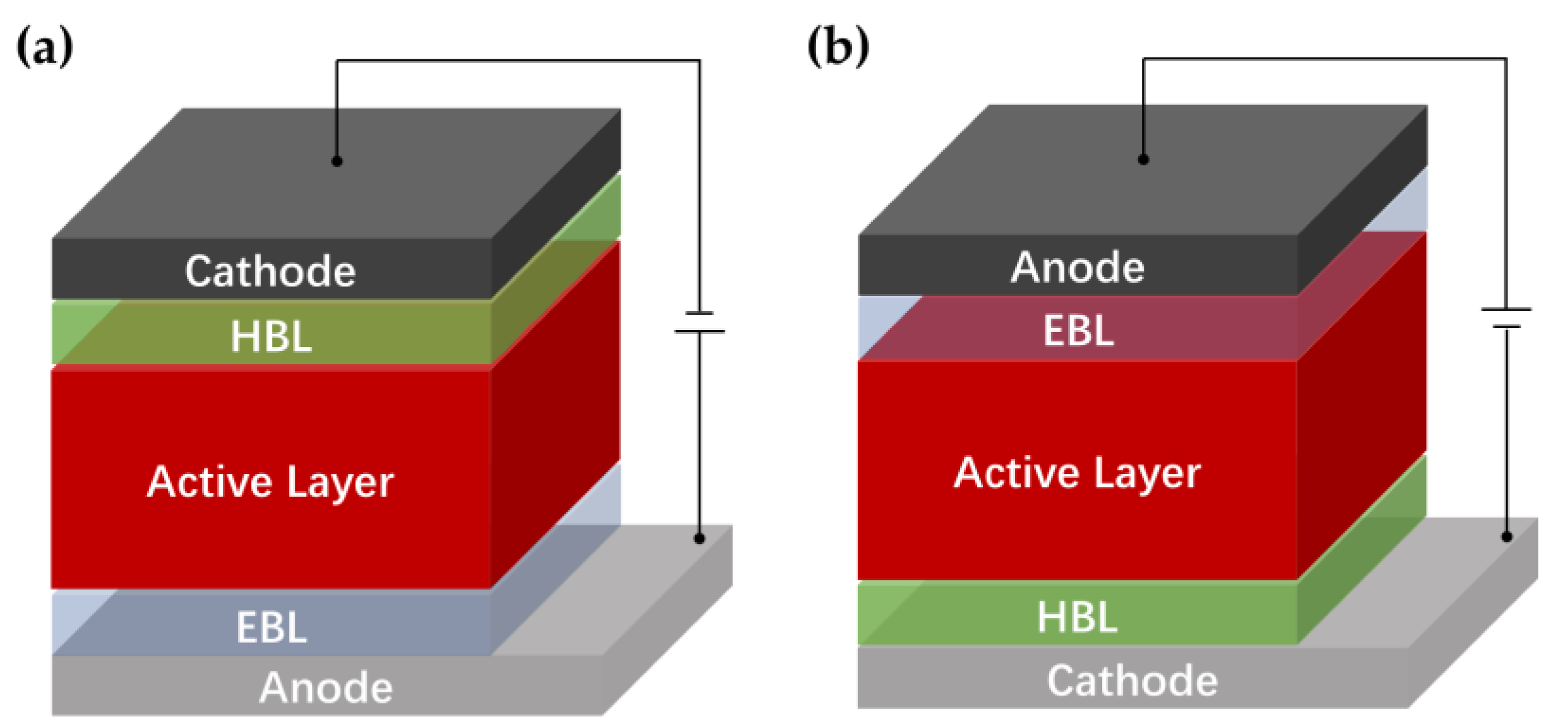
1.4. Blocking Layer Engineering

The single-junction OPD is a sandwich structure, which can be divided into a conventional structure (Figure 3a) of the anode/EBL/active layer/HBL/cathode and an inverted structure (Figure 3b) of the anode/EBL/active layer/HBL/cathode [33], shown in Figure 3. In most devices, the bottom electrode ITO can be used as an anode of conventional OPDs or a cathode in inverted OPDs. In the conventional structure, ITO is generally used as an anode for the collection of holes, and in the inverted structure, it is used as a cathode for the collection of electrons. The two-type structure designed is for the better collection of photogeneration carriers.
Generally, an efficient interface layer should meet several requirements in organic devices. First, it can promote the match of energy levels at the interface with decent electrical properties of high electron/hole mobility and the ability to form an ohmic contact with the adjacent active layer and electrode. These comprise an additional interlayer between the electrode and the photoactive layer, such that ELUMO,HBL > ELUMO,acceptor for electrons and EHOMO,EBL < EHOMO,donor for holes, resulting in an increased energetic barrier for charge injection. Ideally, ELUMO,HBL = ELUMO,acceptor and EHOMO,EBL = EHOMO,donor so that carrier collection is not impeded. Second, there is compatibility and stability with the active material and electrode. Finally, relatively high transparency ensures that the active layer can absorb as much light as possible to achieve optimal performance. To date, some reviews on the interface layer of optoelectronic devices have been reported, including organic (e.g., small molecules, polymers, and organometallic complexes) and inorganic materials (e.g., metal salts and metal oxides).
Considering that these organic devices are generally composed of thin films, their performances are heavily dependent on the interfacial properties, which not only promote the efficient extraction and transport of carriers but also suppress the charge injection under the reverse bias to reduce dark current [26]. Therefore, an ever-increasing number of researchers are working on interface modification, such as HBL and EBL, to improve the performance of OPDs. The interface layers are varied and complex so that it is actually difficult to determine a definite mechanism of one interface material in the device. Some reviews on the interface layer and materials of optoelectronic devices have been reported [34,35,36,37,38,39,40]. Most of them mainly aimed at OPV and focused on some specific interface materials, such as transition metal oxides [34,36], metal oxides [39], two-dimensional materials [38], and conducting polymers [37]. As a device different from OPV, OPDs have unique characteristics in interface engineering. Along with the rapid progress in OPDs, increasingly more interfacial materials have been involved in these devices. In this Review, we aim to provide a summary and discussion on various types of interface (HBLs and EBLs) materials and their latent mechanisms in OPDs. In Section 1, the fundamentals and performance metrics of OPDs will be introduced, and the background and the necessity of blocking layer engineering in OPDs will be presented. Section 2 reviews several carrier blocking layer materials for holes and discusses their modification and performance enhancements in OPDs. Section 3 provides several materials of carrier blocking layer for electrons, resulting in an increased energetic barrier for electrons injection and their applications in OPDs.

2. Materials for HBLs in OPD

The HBL needs not only the ability of hole blocking but also the function of electron transport for OPDs, and it mainly includes organic and inorganic materials. It comprises an additional interlayer between the electrode and the organic photoactive layer, such that EHOMO/CB,HBL < EHOMO,donor for holes, resulting in an increased energetic barrier for charge injection [26]. Ideally, ELUMO,HBL = ELUMO, acceptor so that photogenerated carrier collection is not impeded. HBLs based on organic materials have been extensively investigated because of their light weight, solution processability, and large-scale flexible fabrication methods in recent decades. Inorganic HBL materials are favored because of their very good stability, high carrier transport performance, and little absorption losses, which makes the inorganic interface materials widely used in OPDs.

2.1. Small Molecular Organic Materials

2.1.1. BCP

2,9-dimethyl-4,7-diphenylphenanthroline (BCP) is an organic small molecule material, which was used as the functional layer material in organic light-emitting diode (OLED) in the early stage [41]. The thermal evaporated BCP thin film (~10 nm) is commonly used as an interface layer (HBL) due to its low HOMO energy level of ~6.7 eV [42,43]. In Figure 4a, the dark current of the optimized polymer photodetectors decreased significantly by 1–2 orders of magnitude and this device exhibits specific performance with D* of 1.4 × 10¹² Jones at 800 nm [44]. It is believed that the dark current is dominated by electron injection/transport due to the very large hole barriers from electrode contact or the BCP blocking layer, as shown in Figure 4b. BCP HBL not only has the ability of hole blocking but also has high electron mobility. Guo et al., achieved a higher EQE of over 10,000% photomultiplication-type OPDs with the BCP inserted layer, as indicated in Figure 4c [45]. This work shows that HBL materials with larger HOMO, lower LUMO energy levels, and higher electron mobility should be used for the hole accumulation and electron injection in OPD, as shown in Figure 4d. The organic small molecule BCP has also been used in flexible electronic devices. A lightweight ultraviolet (UV) photodetector has been fabricated with mechanical flexibility and photoresponse stability [46]. The photodetector has a low Jd of 1.3 × 10⁻⁵ mA cm−2 even at −15 V bias due to the blocking capability of BCP and the large hole-injection barrier of 1.3 eV from the Al cathode into the HOMO of poly((9,9-dioctylfluorenyl-2,7-diyl)-alt-co-(bithiophene)) (F8T2).

2.1.2. Bphen

4,7-Diphenyl-1,10-phenanthroline (Bphen) is also an organic small molecule material, which was used as the functional layer material in OLED in the early stage [47]. For the interface layer of OPD, Bphen is used to improve charge carrier transport ability due to its electron-transport capability [48]. The HOMO of Bphen is ~6.5 eV, lower than that of universal acceptor materials (e.g., C60, PC60BM, PC71BM), which can be used as an HBL to reduce dark current under reverse bias in BHJ OPD [49,50,51,52,53]. The optical measurement integration of organic OLEDs and OPDs is implemented with the interface layer of Bphen [3,54]. HBLs of these two optoelectronic devices both use Bphen. Yang et al., demonstrated the broadband visible OPDs with the highest D* reached 2.67 × 10¹² Jones at 710 nm [55], as shown in Figure 5b. In Figure 5a, Bphen is used as an interface layer to reduce the quenching of photo excitons and impede hole injection from the Ag side. Due to the compatibility between the organic small molecule Bphen and vacuum evaporation process, the evaporated OPD was studied. Lee, et al., fabricated the small molecule OPDs by vacuum-processing with Bphen as HBLs [56], and the device configuration, molecular structure, and energy level of the respective materials are displayed in Figure 5c. The experimental results revealed that the photodetector with the best performance at the wavelength of 730 nm achieved a very low Jd of 1.15 × 10⁻⁹ A cm−2 (Figure 5d) and an EQE of 74.6% with a R of 0.439 A W−1 at −2 V bias.

2.1.3. C60

A fullerene, C60, has high electron mobility (1.6 cm2 V−1 s−1) and conductivity (2.3 × 10⁻³ S cm−1), making it an excellent candidate to extract electrons [57]. Due to the electron mobility and deep HOMO level, the C60 layer has been used as an electron transport layer (ETLs) in many organic photoelectric devices [58]. In particular, as HBL in OPDs, C60 is a potential candidate expected to reduce dark current [59,60]. Armin and co-authors fabricated a thick junction broadband OPD with a C60 (35 nm) HBL to provide hole blocking/electron transport at the interface with the cathode [61]. Kim et al., researched broadband OPDs based on a non-polymeric organic semiconductor in Figure 6a [62]. Hole injection was hindered when a thin layer of C60 was added on top of the active layer leading to a lower dark current (0.11 nA cm−2) for devices. In Figure 6b, because of the insertion of the C60 HBL with a deep HOMO level (~6.0 eV), a low-saturation dark current device even with a thin active layer (350 nm) was realized. Joo and co-authors researched a near-infrared organic thin-film (120 nm) photodiode with 3.3 × 10¹² Jones D* and 80% EQE [63].

2.2. Polymer Organic Material

2.2.1. PEIE

It is known that Polyethylenimine ethoxylated (PEIE) can shift the work function and lead to an electron selective contact [64] on various different materials, and this polymer material is coated with a one-step, low-temperature solution process. In particular, the low work function transparent PEIE-modified ITO electrode is expected to reduce the dark current in OPDs due to the formed barrier between the active film and the electrode [65,66,67,68]. Wang et al., reported a high-performance solution-processed polymer photodetector with a PEIE-modified ITO electrode [69]. In Figure 7a, the energy barrier formed between the WF of the PEIE-modified ITO and the HOMO of the donor poly(3-hexylthiophene) (P3HT) is 0.75 eV greater than that of the bare ITO-based device. Therefore, the current density is reduced from 2.25 × 10⁻⁵ A⋅cm−2 to 8.79 × 10⁻⁷ A⋅cm−2 at −0.5 V, as presented in Figure 7b. In addition, PEIE can lower the work function of the Poly(3,4-ethylenedioxythiophene)–poly(styrenesulfonate) (PEDOT:PSS) electrode. However, the conventional spin coating process cannot effectively fabricate an adjustable PEIE thin film on PEDOT:PSS due to the solvent orthogonal. The printability of PEIE enables the large-area OPD to be prepared by the solution method [70,71]. Pierre et al. realized all-printed organic photodiodes with the blade-coated PEDOT:PSS/PEIE cathode by changing the weight concentration of PEIE in the blade-coated solution (Figure 7c) [70]. By changing the PEIE solution concentration between 0.05% and 1 wt%, the work function of PEDOT:PSS was able to decrease from 5.15 eV to anywhere between 4.6 and 4.1 eV, and all-printed OPD arrays were obtained with an average D* as high as 3.45 × 1013 cm Hz0.5 W−1 under a bias of −5 V (Figure 7d). Because PEIE has good transmittance in both visible and infrared wavelengths, the PEIE HBL is also used in near-infrared OPDs [72,73].

2.2.2. PFN

The water/alcohol soluble conjugated polymer, poly((9,9-bis(3′-(N,N-dimethylamino)propyl)-2,7-fluorene)-alt-2,7-(9,9-dioctylfluorene)) (PFN) is commonly reported as an interfacial layer for enhancing electron collection in organic solar cells (OSCs) [74]. Some works show that OPDs with PFN as the interfacial layer can work well under forward and reverse bias [75]. Miao et al., used PFN as the anode buffer layer to demonstrate efficient OPDs based on P3HT and non-fullerene [76]. As shown in Figure 8, the value is (about) 0.9 eV between the HOMO levels of ITO and PFN under forward bias and between the HOMO levels of Al and P3HT under reverse bias. In the dark, a large interfacial barrier of 0.9 eV results in hardly hole injections under both forward and reverse bias (Figure 8a,b). With light illumination, trapped electrons in the 3,9-bis(2-methylene-(3-(1,1-dicyanomethylene)-indanone)-5,5,11,11-tetrakis(4-hexylphenyl)-dithieno (2,3-d:2′,3′-d′)-s-indaceno(1,2-b:5,6-b′)dithiophene) (ITIC) near the Al electrode encourage hole tunneling injection and form an external circuit (Figure 8c,d). Wang et al., fabricated the OPDs based on a conventional P3HT/(phenyl-C61-butyric-acid-methyl-ester) (PC61BM) bulk heterojunction by incorporating a PFN interlayer between the anode and the active layer [77]. The Jd was effectively reduced from 0.07 mA cm−2 to 1.92 × 10⁻⁵ mA cm−2 under a −0.5 V bias. The holes would pile up close to the PFN and the active layer interface due to the dipole layer of PFN and then create an interfacial band bending leading to a tunneling electron injection to the active layer. Furthermore, Zhong’s team and Xie’s group used a thin layer of PFN-Br as the cathode interlayer layer to facilitate charge collection and prevent the potential diffusion of metal electrodes during evaporation [6,78].
Photomultiplication-type organic photodiodes (PM-OPDs) can be a promising candidate for the commercialization of OPDs based on their self-signal amplification behavior. In BHJ PM-OPDs, it was revealed that Bromide of PFN (PFN–Br) not only reduced the work function of ITO to achieve effective Schottky junctions with polymer donor materials, but also efficiently enhanced the trapping efficiency, which can be ascribed to electrostatic interactions between the positively charged quaternary ammonium groups and trapped electrons within the isolated (6,6)-phenyl C71 butyric acid methyl ester (PC71BM) domains. Zhu’s group prepared the near-infrared and visible light dual-mode OPDs and PFN-Br using a modified ITO anode to create an interface dipole, assisting in bidirectional tunneling hole injection [2].

2.2.3. PEI

The polyelectrolyte material polyethylenimine (PEI) is of great interest for its advantages of low cost, environmentally friendly, and solution-process compatibility. PEI can reduce the work function of electrodes by forming surface dipole moment [79]. Falco et al., sprayed deposition of PEI thin films for the fabrication of fully-sprayed organic photodiodes [80]. In this work, the feasibility of smooth, reliable, and effective spray-coated thin PEI layers was first to demonstrate that exhibit performance comparable to analogous spin-coated films in fully sprayed OPDs. Because the PEI has a good solution processing ability, Grimoldi et al., reported on the successful reduction of dark current below 100 nA cm−2 (at −1 V bias) and preserved a high quantum yield (65%) in an inkjet-printed photodetector by the insertion of an electron blocking layer based on PEI [81]. Cesarini et al., fabricated high-performance fully printed organic photodiodes on flexible substrates through the use of a PEI interlayer [82]. Controlling solution composition and deposition parameters for this layer, a 57 nA cm−2 Jd was achieved with dramatic improvements in process yield (from less than 20% to more than 90%).

2.3. Inorganic Oxide Semiconductor Materials

2.3.1. ZnO

Zinc oxide (ZnO) is the most commonly used ETLs in organic optoelectronic devices. In particular, ZnO layer with a wide band gap can modify both the cathode and anode in OPDs. In inverted OPDs, the ZnO layer is prepared on the bottom electrode, generally between the ITO and the organic layer. Inverted organic optoelectronic devices are more stable and have been extensively studied [33]. For those OPDs, the devices with a ZnO interlayer can usually obtain a lower dark current, an enhanced D*, and an improved EQE [83]. As shown in Figure 9, for the OPDs based on poly((4,8-bis((2-ethylhexyl)oxy)benzo(1,2-b:4,5-b’) dithiophene-2,6-diyl)(3-fluoro-2-((2-ethylhexyl)carbonyl)thieno(3,4-b)thiophenediyl)) (PTB7):PC71BM in the dark under reverse bias, the ZnO layer can effectively block the hole injection from ITO into the HOMO of PTB7 due to the large barrier of ~2 eV between ITO and ZnO in Figure 9a, and then the low dark current will be obtained. Under illumination, the photogenerated electrons on the PC71BM LUMO can easily move from the ZnO layer to the ITO electrode under a reverse bias as shown in Figure 9b, which is contributed to obtain the fast photoresponse.
For instance, n-type ZnO was selected as the HTL in a semi-tandem structure OPD [84]. The high electron injection barriers enable a Jd as low as 6.51 × 10⁻⁵ mA cm−2 at −0.1 V, resulting in a noise current of 3.91 × 10⁻¹³ A Hz−1/2 at 70 Hz. Since ZnO nanoparticles are stable in the solvent, a print ink was prepared for full-print OPDs. Eckstein et al., proposed a ZnO-nanoparticle-dispersion diluted with butanol in a ratio of 1:2 for use as the electron extraction layer to form a fully digitally printed 2D image sensor [85]. The individual OPD pixels exhibited a state-of-the-art LDR (114 dB), SR (0.3 A W−1), D* (2 × 10¹² Jones), not only as HBLs, but also to enhance the device response to UV light, because of ZnO absorption in the UV band [17,86,87]. Ma’s group demonstrated a narrow-bandgap OPD had a significant increase in photocurrent upon UV light exposure using ZnO nanoparticles as an anode interfacial layer [88]. Ultrahigh EQE of 140,000% was achieved in this device with 30 s UV light irradiation. This phenomenon is attributed to the UV light illumination-induced oxygen molecule desorption from the surface of ZnO nanoparticles, which reduces the electron injection barrier at the anode interface.
ZnO has been widely used as an ETL in OPDs due to its matched work function, high electron mobility, solution processability, and high transparency. However, the size of the sol-gel ZnO nanoparticles is much larger, which may lead to larger interstitial regions and pinholes in the film that negatively affect electron mobility and make the active layer more susceptible to the effects of water and oxygen [89]. By introducing a polymer into the ZnO nanoparticles, a new strategy to prepare ETLs is produced in OPDs [90]. Zhao et al. realized a low dark current and high photo D* transparent organic ultraviolet photodetector by using polymer-modified ZnO as the HBL [87]. The result shows that the aggregation of PFN can cause the surface defects to enhance the possibility of charge carrier trapping, responsible for a lower dark current density. With this combination, a maximum D* of 1.58 × 10¹² Jones with the fourfold improvement compared with the OPD without PFN has been achieved. The PEIE is also used to modify the ZnO layer in OPDs. Vandewal’s group fabricated infrared OPDs with the ZnO/PEIE HBL, which have the potential to be a useful detector up to 2000 nm [91]. Opoku et al., presented an inverted OPD based on PBDB-T: PC61BM and with a low work function PEIE-modified ZnO on an ITO cathode. This device showed a comparatively broader photoresponse and better performance, with specific D* of 3.749 × 10¹² and EQE of 62% at a bias voltage of 2 V. Xia et al., demonstrated all-polymer and semitransparent OPDs fabricated through lamination on flexible substrates with high D* up to 1011 Jones [92]. By introducing the PEI between the active and ZnO layer, this lamination method is roll-to-roll compatible and combined with flexible substrates and is getting close to low-cost, large-scale production.

2.3.2. TiO2

Titanium oxide (TiO2) is a metal oxide as an efficient ETL because of its high electron mobility, high stability, low-cost, good transparency, and safety for both humans and the environment due to the good match conduction band (~4.4 eV) with the LUMO of PCBM (~4.3 eV) and the deep valence band (~7.5 eV) formed energy barrier Φb for effectively blocking the holes. By changing the deposition methods and precursor solvents to tune the forming environment, TiO2 has four commonly crystal types: anatase (tetragonal), brookite (orthorhombic), rutile (tetragonal), and TiO2 (B) (monoclinic). It is widely believed that anatase is preferred over the other crystal types for photoelectronic device applications because of its higher electron mobility and low dielectric constant [93]. Recently, TiO2 has been prepared in the form of nanoparticles, nanocrystals, nanotubes, and nanorods [94,95]. The sol–gel method is one of the most widely used conventional methods in the chemical synthesis of TiO2 for organic optoelectronic devices [96,97]. This method provides the advantages of homogeneous products and allows the formation of complex shapes. The general preparation procedures are outlined by Jensen et al. [98]. This study addresses the nonaqueous sol–gel synthesis of nanocrystal anatase TiO2 and it yields particles 3–7 nm in size.
The early application of TiO2 nanocrystals as the electron extraction layer (HBL) in OPDs was reported by Wallace C’s group in Figure 10 [99]. In this case, a clear dark current rectification ratio of approximately 10 at ±1 V is achieved, and the on/off ratio is as high as 105 by incorporating the TiO2 (~20 nm), as shown in Figure 10b. In Figure 10c, the effective injection barrier between active and electrode induced by trap states in TiO2 will impede charge injection into the device, and thus very low dark current can be obtained [100]. After photogeneration, part of the free electrons are trapped at surface sites and the rest are trapped in the bulk [101]. The shallow bulk trapped electrons relax into deeper bulk sites through a hopping process in Figure 10d. As the occupation increases, the proportion of shallow trapped carriers becomes dominant, resulting in increased mobile charge carriers and their mobility [102,103]. These increased mobile charge carriers will make the Fermi level rise and reduce the work function of TiO2, which will lower the effective barriers at the TiO2 interfaces. Deng’s group introduced ligand-free anatase TiO2 nanocrystals with a clean surface and excellent electron extraction [104]. The grain size of the anatase TiO2 nanocrystals is about 4.0 nm, and the surface roughness of the film is about 1.201 nm. By introducing the trap states between the TiO2 nanocrystals and the photoactive layer of P3HT:PC61BM, the OPD shows low Jd (3.98 × 10⁻⁷ A cm−2) and high D* (1.9 × 10¹² Jones) at −1 V.
In addition, the planar HBL based on nanostructured TiO2 has also been introduced in OPDs. By using certain nanostructure materials, the interfacial area between the blocking layer and active layer can be further enlarged. Deng et al., reported aligned nanofibers of TiO2 prepared by electrostatic spinning technology as an interfacial layer that can significantly enhance the performance of inverted OPDs [10]. The performance of the devices with TiO2 nanofibers in different arrangements (Figure 11a–c) as the interfacial layer was investigated, and the results exhibited that photodetectors with one-way nanofibers had the highest D* of 2.93 × 10¹³ Jones in Figure 11c,d. The enhancement of the performance was attributed to better crystallization of one-way nanofibers of TiO2, which facilitate charge separation at the electrode−active interface and electron transport within the interfacial layer.

2.3.3. SnO2

Stannic oxide (SnO2) is another wonderful ETL for photoelectric devices, such as perovskite solar cells, which have a better band alignment with the perovskite layer and high electron mobility of up to 240 cm2 V−1 s−1, which is helpful for electron extraction [105]. Besides, SnO2 is easily processed by low-temperature methods (<200 °C), which is compatible with the flexible device and large-scale commercialization [106]. The SnO2 layer can efficiently block the external charge injection, which considerably reduces the dark current density in the OPDs. Deng et al., realized a high-performance polymer photodetector using the non-thermal-and-non-ultraviolet–ozone-treated SnO2 nanoparticle film between the ITO electrode and the active layer of the P3HT:PCBM blend [107], and the device structure is shown in Figure 12a. In Figure 12b,c the SEM image shows that the untreated SnO2 nanoparticle can efficiently form continuous and dense films, and the transmittance spectrum indicates that there is almost no absorption loss when the incident light passes through the non-thermaland-non-UVO-treated SnO2 layer into the P3HT:PCBM layer. The Jd of the OPD can be effectively reduced from 1.94 × 10⁻¹ to 2.89 × 10⁻⁴ mA cm−2, and the photocurrent density of the device can be significantly increased from 9.63 to 156.63 mA cm−2 under −1 V bias, as shown in Figure 12d. According to the working mechanism of the device, the effective injection barrier between the ITO and the untreated SnO2 film and the trapped states between the SnO2 film and the photoactive layer can significantly impede the charge injection into the device under reverse bias (Figure 12e), leading to a low dark current. The photogenerated charge carriers at the interface between the SnO2 and the photoactive layer are trapped due to the defects induced by the non-thermal-and-non-UVO-treated SnO2 and the trapped photogenerated electron accumulation at the interface results in a band bending (Figure 12f) [99]. In addition, the conductivity of SnO2 increases and the electron injection barrier from ITO to SnO2 decreases when the trapped states of the SnO2 film are occupied by the charge carriers [88]. Therefore, a large number of electrons can tunnel into the device, leading to a significant photocurrent.
Huang et al., demonstrated an alternative ETL, SnO2, which rendered the dark current characteristics minimally sensitive to illumination processes [108]. By using a simple “double”-layer strategy for the SnO2 ETL, the magnitude of the dark current can be suppressed to below 10 nA cm−2, close to the initial dark current exhibited by the ZnO-based devices without UV exposure history. The original outstanding photoresponse was not compromised with the use of the alternative ETL.

2.4. Inorganic Salts

The inorganic salts used as the interfacial materials mainly contain alkali carbonates and alkali metal halides. Alkali carbonates, such as Cs2CO3, are employed to modify the electrode and blocking carriers in OPDs. Between the electrode and active layer, its appearance can form a dipole moment at the interface, which causes the potential change to increase the holes’ transport energy barrier and to inhibit the recombination of holes by the anode. Guo et al., reported a blue light-sensitive OPD with a thickness of 2 nm Cs2CO3 HBL [109]. The device showed a Jd of ∼21 nA cm−2 at the bias of −3 V, which might be attributed to the carrier injection barrier formed at the interface between the electrode and the sensitive layer.
The halide salt mainly improves the performance of the photovoltaic device by adjusting the work function of the electrode effectively. Above all, the most common type of these is the LiF, which is widely introduced between the Al electrode and active layer to hinder metal diffusion inside the photoactive matrix [110,111,112]. Zafar et al., presented ternary blend-based bulk heterojunction poly(2,7-(9,9-di-octylfluorene)-alt-4,7-bis(thiophen-2-yl)benzo-2,1,3-thiadiazole) (PFO-DBT): poly(2-methoxy-5(2’-ethylhexyloxy) phenylenevinylene (MEH-PPV):PC71BM organic photodetector [113]. A thin film of LiF (~10 Å) was used between the active layer and top electrode to enhance the performance of the OPD, due to lowering of the effective work function of the top Al cathode and protection of the photoactive layer from hot Al atoms during their evaporated deposition. Esopi et al., fabricated an organic photomultiplier photodetector utilizing F8T2:PC71BM blend active layers with weight ratios of 100:1 and 100:4, with and without the presence of an ETL/HBL of LiF [114]. Generally, devices with LiF are more stable, and reach an EQE and R of 5600% and 15.9 A W−1, respectively, under 360 nm illumination and a −40 V applied bias and an extremely low dark current of 2.7 × 10⁻⁷ mA cm−2 at a −1 V bias. The device structure and working mechanism are shown in Figure 13. Without or with a reverse bias (Figure 13b,c, respectively), the large hole injection barrier of 1.2 eV from the Al cathode into the HOMO of F8T2 can effectively block hole injection in the dark. Under illumination, these trapped electrons in PC71BM (Figure 13d) near the LiF-modified Al cathode cause the active layer energy bands to bend at the interface with a reverse bias, which lowers the tunneling distance and therefore the barrier for holes to inject from the Al cathode into the HOMO of F8T2 (Figure 13e).

3. Materials for EBLs in OPD

The EBLs are in an equal position with HBLs in the OPDs while they serves to extract holes from the organic active layer to the electrode and inhibit the passage of electrons. Similar to the HBLs, some rules should be considered in the design of EBL materials, such that ELUMO/VB, EBL > ELUMO, acceptor for electrons, resulting in an increased energetic barrier for electron injection. Ideally, EHOMO/CB,EBL = EHOMO, donor so that photogenerated carrier collection is not impeded [26]. There are some EBL materials that mainly include organic and inorganic materials in OPDs.

3.1. Small Molecular Organic Materials

3.1.1. TFB

The polymer poly(9,9′-dioctylfluorene-co-N-(4-butylphenyl)diphenylamine) (TFB) is used as an interlayer and it is deposited by a solution-based technique in an organic photoelectric device [115]. Some devices with the interlayer have a significant enhancement due to TFB, which can reduce the WF of the Al electrode. TFB is also deposited on ITO and the PEDOT:PSS electrode to form a barrier against the injection of electrons in OPDs [116,117]. It could provide better energy level alignment with the LUMO of PC71BM and thereby lead to an improvement in the BHJ device containing fullerene derivatives. Keivanidis et al., presented a solution-processed OPD with Jd values as low as 80 pA mm−2 and a corresponding EQE of 9% [118]. The dark current density of the F8BT:PDI devices is reduced by a factor of ten when a thin TFB EBL acts as a barrier against the injection of electrons from PEDOT:PSS to LUMOPDI. Tedde and co-authors reported spray-coated large-area organic photodiodes based on a polymer (Lisicon PV-D4650):PC61BM with the TFB interface layer on the ITO electrode [119]. The values are comparable to commercially available state-of-the-art solid state photodetectors with Jd down to 34 pA cm−2 and a maximum R of ≈0.44 A W−1 (660 nm) under reverse bias conditions of −5 V.

3.1.2. TIPS Pentacene

Triisopropylsilylethynyl pentacene (TIPS pentacene) is a solution-processed small molecule organic material that is mainly used as an interlayer to enhance the mobility in the fabrication of organic thin-film transistors (OTFTs) [120]. Thanks to its HOMO level of 5.3 eV and LUMO level of 3.1 eV [121], this molecule can be used as an electron blocking interlayer sandwiched between a P3HT: PCBM BHJ and an ITO electrode. In OPDs, the devices with TIPS pentacene EBL present a hysteresis behavior under dark conditions with reverse bias. Tedde et al., reported a conjugated donor−acceptor polymer, poly-(4,4,9,9-tetrakis(4-hexylphenyl)-4,9-dihydro-s-indaceno(1,2-b:5,6-b′)dithiophene-2,7-diyl-alt-5-(2-ethylhexyl)-4H-thieno-(3,4-c)pyrrole-4,6(5H)-dione-1,3-diyl) (PIDT-TPD):PC61BM solution-processed OPDs with the TIPS pentacene interlayer [122]. As shown in Figure 14, the TIPS pentacene interlayer exhibits a high LUMO level (−3.1 eV) and acts as an EBL, which is crucial for reducing the Jd (3 mA cm−2 at −5 V bias). The photogenerated carriers are driven by the external negative bias and drift to the respective electrodes under the extraction of the TIPS pentacene layer in the OPD at reverse bias, and the device shows an EQE of 52.5% at 610 nm. TIPS pentacene, as a beneficial interlayer for OPDs in imaging applications, has been researched [123]. Benavides et al., reported OPDs with dark currents of∼0.9 nA cm−2 at −5 V and EQE close to 80% at 530 nm and integrated on top of amorphous silicon thin-film transistor backplanes to obtain the OPD-based image sensor using this interlayer. Compared to the reference, P3HT interlayer, TIPS pentacene shows a significant increase in the OPD’s D* from 3.29 × 10¹² to 1.63 × 10¹³ Jones.

3.2. Polymer Organic Material

3.2.1. PEDOT:PSS

PEDOT:PSS is the conjugated polymer, which is most widely used as EBL to block the transportation of electrons and transport holes in OPDs. It is always composed of poly(3,4-ethylenedioxythiophene) (PEDOT) doped with poly (styrene sulfonate) (PSS), and the PSS is used to improve conductivity and solubility. PEDOT:PSS is widely used in inverted and conventional OPDs because it is strictly solvent orthogonal to the organic BHJ layer. Bouthinon et al., fabricated conventional and inverted OPD with the PEDOT:PSS layer to collect holes [124]. This work brings new elements in the understanding of the impact of oxygen contamination in the performance degradation of organic solar cells or photodiodes. In conventional OPDs, using PEDOT:PSS as the anodic interface to modify ITO could reduce the oxidation potential, enhance conductivity, and is beneficial to the transport of holes and energy level matching [125,126,127]. Zhang’s group [128] reported the ternary OPDs used one interface layer of PEDOT:PSS, which have similar EQE values of ≈2000% and specific D* larger than 1011 Jones at −50 V bias under the bottom and top illumination conditions. For inverted OPDs, the EBL is deposited on the organic layer and top electrode, and it is required that the preparation of this interface layer does not destructively affect the active layer. Wagner et al. realized semi-transparent inverted organic detectors with a 50 nm PEDOT:PSS layer, which used solution-based fabrication and exhibited an overall transmittance of about 20% in the visible range of the electromagnetic spectrum [129].
Some groups modified PEDOT:PSS to improve its hole extraction rate and conductivity or change its WF by adding some additives into PEDOT:PSS. P-type inorganic nanoparticles doped into PEDOT:PSS to form a composite interface layer is a potential strategy. Hu’s work [130] demonstrated the work functions of amino acid functionalized graphenes (GO–Cys), and their compounds with PEDOT:PSS were tuned over a wide range, which matched well with the energy of BHJ organic materials. As shown in Figure 15a,b the GO–Cys sheet is tightly covered by the PEODT:PSS, leading to the formation of a contiguous film, and the OPDs exhibited a remarkably low Jd of 4.4 × 10⁻¹⁰ A cm−2 at 0 V the highest normalized D* of 5.7 × 10¹² jones at −0.1 V (Figure 15c,d). Abdullah’ group showed that the composite of V2O5 and PEDOT:PSS was introduced as EBL in the OPD [131]. The resultant device had the ITO/PEDOT:PSS+V2O5/PCDTBT:PC71BM/V2O5/Al architecture and exhibited a new range of photo-currents as well as showed an enhanced photo-response.

3.2.2. Donor Materials of BHJ

The BHJ in OPDs consists of donor and acceptor materials, which can effectively promote photon absorption and exciton separation to improve device performance. The donor and acceptor materials not only generate free carriers but also transport carriers under illumination. In particular, the electrons are transported in the high mobility n-type layer (acceptor) and holes are transported in the high mobility p-type layer (donor) in PHJ OPDs. The p-type donor material is a potential interfacial EBL in BHJ OPDs [132]. However, the spin-coated donor materials with the BHJ material systems can lower the device performance, because the cross-linking or orthogonal solvent can dissolve or damage the pre-deposited active layer.
A conjugated polymer, P3HT, is an earlier and more common donor material in BHJ organic devices. Xiong et al., introduced a universal strategy of transfer-printing P3HT as the EBL to realize highly sensitive photodetectors [133]. The transfer printing of the P3HT uses poly(dimethylsiloxane) (PDMS) as the transfer medium. The fabrication procedure and a schematic demonstrated the P3HT layer blocks the electron injection under reverse bias, shown in Figure 16. This approach tactfully circumvents the requirement of the solvent orthogonality between the active layer and the P3HT. The insertion of the P3HT EBL substantially reduces the dark current by about three orders of magnitude compared with the photodetectors without the EBL, because it has high-lying LUMO for electron blocking and high hole mobility for hole transport and collection. Inganäs’s group also demonstrated EBLs of P3HT and poly((2,6-(4,8-bis(5-(2-ethylhexyl)thiophen-2-yl)-benzo(1,2-b:4,5-b′)dithiophene))-alt-(5,5-(1′,3′-di-2-thienyl-5′,7′-bis(2-ethylhexyl)benzo(1′,2′-c:4′,5′-c′)dithiophene-4,8-dione)) (PBDB-T) could successfully form on the active layers by using a transfer-printing technique [134]. These inverted all-polymer OPDs exhibit outstanding EQE over 70%, low Jd of 1.1 × 10⁻⁸ A cm−2, and high D* over 3.0 × 10¹² Jones with a planar response over the entire visible range. The aerosol-jet technique is another process to print multilayers from the same solvent system. Hernandez-Sosa and co-authors allowed deposition onto a P3HT-based BHJ without negatively affecting OPD performance [135]. This donor EBL yielded a noise reduction of two orders of magnitude in OPDs operated under −2 V bias.

3.3. Inorganic Oxide Semiconductor Materials

P-type semiconductors are used as the HTL materials of optoelectronic devices because of their unique carrier transmission characteristics. p-type metal oxides, such as NiOx, MoO3, V2O5, and WOX, are competitive materials that currently work as an anode interfacial layer. To some extent, the devices with those metal oxides have similar or better performance compared with those with the most widely used PEDOT: PSS, and the lost-cost synthesis and simpler deposition make them more competitive in mass production.

3.3.1. NiOx

Nickel oxide (NiOx) has a cubic structure similar to NaCl, with a lattice parameter of 0.4173 nm [136]. The non-stoichiometric NiOx with excess oxygen makes it have a certain number of Ni vacancies, so it will produce holes, making a p-type semiconductor. The large band gap (3.7 eV) of NiOx and interfacial dipole (≥0.6 eV) with the organic active layer leads to a hole-selective interface [137]. For OPD, different device structures (conventional and inverted) use different preparation processes for the NiOx EBL. One method under the vacuum system is that NiOx films were prepared by thermal evaporation of Ni and then annealed at high temperature. Lim et al., reported a conventional OPD using a NiOx anode interlayer to reduce the leakage current [138]. In this work, Ni layers were thermally evaporated in high vacuum at 10−6 Torr onto ITO films on glass substrates and then oxidized by heat treatment at 400 °C for 3 h. The D* of the devices is 2.15 × 10¹² jones, which also have an impressive cut-off frequency of 173.15 kHz at −1 V despite a relatively lower light intensity, which is related to the rapid charge extraction ability of NiOx films.
Sol–gel methods have been commonly employed to deposit the NiOx films, due to their simple process and good reliability. Manders and co-authors realized low-noise multispectral photodetectors based on all solution-processed inorganic semiconductors with solution-derived NiOx as the EBL [139]. Kim et al., used Ga-doped nickel oxide (NiOx) for the EBL and investigated the physical effects of Ga doping on the performance of the organic photodiode [140]. It can be discussed that the leakage current of the OPD with Ga-doped NiOx was significantly decreased owing to the increased LUMO level of this layer. NiOx films can also be deposited through spin-coating with suspensions of pre-synthesized nanoparticles. In this case, NiOx nanoparticles are synthesized and dispersed first, which is a critical step to prepare the functional layer. Li et al., proposed a room-temperature NiOx film synthesized from a NiC2O4 precursor via hydrothermal treatment and applied it as an EBL to fabricate OPDs [141]. In this work, smaller and more uniform NiOx nanoparticles (5–10 nm) were obtained and demonstrated a high performance OPD, including a Jd of 1.13 × 10⁻⁷ A cm−2, D* of 3.86 × 10¹² Jones, R of 0.74 A W−1, and 0.5/8 ms at −5 V (Figure 17). Based on this method, Li and co-authors combined the ultra-small nanoparticles with flexible OPDs [142]. This flexible OPD exhibits outstanding mechanical flexibility following tests with 60,000 bends.

3.3.2. MoO3

Molybdenum oxide (MoO3) is a typical p-type metal oxide, which has high hole mobility. This metal oxide is been shown to be an interesting alternative to replace PEDOT:PSS as a hole-injection or hole-extraction layer for OLEDs [143], OTFTs [144], and OPVs [145], and OPDs [146]. MoO3 has good hydrophilia with the organic layer and is widely used as EBLs in inverted OPDs. In those devices, highly stable electrodes (ITO, Ag) were used, and the interlayer (MoO3) was deposited between the active and Ag layer to enhance the stability. Yoon et al., designed a high-performance red-selective thin-film OPD with a dual-band absorbing poly((2,5-bis(2-hexyldecyloxy)phenylene)-alt-(5,6-difluoro-4,7-di(thiophen-2-yl)benzo(c)(1,2,5)-thiadiazole)) (PPDT2FBT) [147]. The MoO3 layer was introduced as the EBL and modified the work function of the Ag electrode from −4.2 eV to −5.0 eV, which is beneficial to suppress dark current and enhance the reception of holes. Based on this structure, red-selective OPDs with a high peak D* above 3.0 × 10¹² Jones with suppressed dark currents (5.9 × 10⁻⁹ A cm−2) were realized. Hwang et al., fabricated an inverted OPD by blending poly(4,8-bis(5-(2-ethylhexyl)thiophen-2-yl)benzo(1,2-b:4,5-b‘)-dithiophene-co-5-(2-hexyldecy1)-1,3-bis(6-octylthieno (3,2-b)thiophen-2-yl)-4H-thieno (3,4-c)pyrrole-4,6(5H)-dione) (PBDTT-8ttTPD) and PC71BM and inserting an 8 nm MoO3 EBL. This OPD shows promising photodetecting properties having a low Jd of 3.72 × 10⁻⁹ A cm−2 and high R of 0.39 A W−1 by varying the thickness of the active layer (260−1100 nm).
OPDs have been actively studied as potential low-cost, high-performance alternatives to amorphous silicon (a-Si) photodiode for flat panels. The top illuminated OPDs are necessary to the image array because the a-Si thin-film transistor (TFT) backplane is almost opaque to visible light [5]. The PEDOT:PSS and ultra-thin metallic films can be used as a transparent electrode in these devices, but there are some potential problems, such as the acidity of PEDOT:PSS and the reflection from the metal surface. Kim et al., reported the top anode OPD with MoO3/Ag/MoO3 semi-transparent electrode for top illumination to yield a high D* of 5.25 × 10¹¹ Jones [148]. In Figure 18, the top MoO3 layer acts as the passivator to the top electrode, and the bottom MoO3 layer not only transmits the incident light but also transports the photogenerated charges. Some image arrays have been realized based on this novel structure. Tessler and co-authors fabricated a hybrid image sensor of small molecule organic photodiode on CMOS [149]. The OPDs used C70 as an electron acceptor, a thick TAPC as hole acceptor, and a transparent anode consisting of MoO3 (10 nm)/Ag (12 nm)/MoO3 (32 nm).

3.3.3. V2O5

As one of the most important semiconductor nanomaterials, V2O5 with a work function of ~5.15 eV and a bandgap of ~2.3 eV was demonstrated to be one of the most promising carrier transport materials [150,151]. There are many studies show that V2O5 deposited by various methods can be used as an alternative HTL in optoelectronic devices [152,153,154]. Gevorgyan’s group fabricated flexible OPD devices with industrial-scale manufacturing techniques such as slot-die coating and demonstrated their use in proximity and light-sensing applications [155]. They studied optimizing the slot-die-coated hydrated, processed using a roll coater and investigated the interfacial properties of V2O5 with impedance spectroscopy to reveal the loss mechanisms in the electrical properties. Although devices incorporating V2O5 semiconductor nanomaterials possess better stability in their lifetime, they in general, as a single HTL material, lag behind the PEDOT:PSS HTL because of the non-ideal inorganic nanoparticle film interface. Abdullah [131] combined V2O5 along with PEDOT:PSS to form an organic-inorganic composite layer and expected that the composite layer would complement the drawbacks of single V2O5 and conventional PEDOT:PSS. Analysis of the surface roughness over a scan area of 2 μm × 2 μm indicates root mean square (RMS) surface roughness values of 1.27, 2.03, and 4.28 nm for the pristine PEDOT:PSS, composite, and pure V2O5 layer, respectively. The obtained performance of the device indicates that the incorporation of V2O5 in PEDOT:PSS to form a composite EBL led to an enhanced photo-response at −1 V, which is desirable for light-sensing applications.

3.4. Inorganic Salt

At present, the research works on the electron barrier are relatively limited in OPDs. Recent progress indicates that copper(I) thiocyanate (CuSCN) exhibited great potential as the anode interfacial layer due to its good hole mobility, high optical transparency, and remarkable electron blocking ability on account of its relatively shallow conduction band [156,157]. CuSCN has been successfully used in OLEDs and PSCs as HTL, enabling remarkable performance [158]. Huang et al., developed high-performance near-infrared OPDs with the CuSCN interface layer [21]. As shown in Figure 19a, the relatively shallow conduction band of CuSCN resulted in a much higher electron-injection barrier from the anode and shunt resistance compared with PEDOT:PSS, and presented similar optical properties. These features led to the dramatically reduced Jd of 2.7 × 10⁻¹⁰ A cm−2 and an impressively high specific D* of 4.4 × 1013 cm Hz1/2 W−1 at 870 nm with −0.1 V bias (Figure 19b). Tessler and co-authors reported the dependence of the reverse bias dark current of an acceptor C70-based PHJ diode on different donor molecules with a 70 nm solution deposited thick film of CuSCN as the EBL [30]. An inverted small molecule organic photodiode with the structure TiN/CuSCN (80 nm)/TAPC (50 nm)/C70 (50 nm)/BCP (8 nm)/Mg (30 nm)/Ag (70 nm) was further fabricated by his group [159].

4. Conclusions and Outlook

In this article, we have provided a brief summary of recent progress on different types of blocking layer materials, which have been demonstrated to play a critical role in OPDs. At present, the interface layer materials in organic solar cells and OPDs have great similarities. However, due to the different working mechanisms of devices, not all materials can be used in OPDs. Therefore, more research and optimization of these materials should be carried out for OPDs. From Table 1 and Table 2, we can ascertain the development of OPDs in hole and electron blocking layer materials in recent years, respectively. However, more efforts are needed to promote their applications and to propose new materials for OPDs.
(1)
Organic interface materials in OPDs are expected to be used in future flexible wearable electronic devices, and further research is needed. However, it is necessary to develop new strategies to solve the problem that they are orthogonal to the solvent of the organic active layer according to the device structure.
(2)
Inorganic materials have also been studied extensively in OPDs because of their high stability. However, the particle size of the material needs to be further reduced, and there are still relatively few p-type inorganic nanomaterials for EBLs. How to achieve the preparation of high-quality inorganic blocking layers at low temperature or even room temperature is the focus of our attention.
(3)
Doping is one of the straightforward ways to modify the carrier blocking layer. The method of inorganic nanoparticle doping in organic interface materials is expected to be used in the future research of OPD because it combines the advantages of the two types of materials.

Author Contributions

Conceptualization, Y.L. and J.Z.; formal analysis, investigation, Y.L. and H.C.; resources, Y.L.; writing—review and editing, Y.L. and J.Z.; supervision, J.Z.; funding acquisition, J.Z. All authors have read and agreed to the published version of the manuscript.

Funding

This research was funded by the National Natural Science Foundation of China (51725505), National key research and development program of China (2017YFB0404703), Shanghai Industrial foundation project (GYQJ-2018-2-04), and Shanghai Science and Technology Funds (17DZ1930502).

Data Availability Statement

No new data were created or analyzed in this study. Data sharing is not applicable to this article.

Conflicts of Interest

The authors declare no conflict of interest.

References

  1. Shi, L.; Liang, Q.; Wang, W.; Zhang, Y.; Li, G.; Ji, T.; Hao, Y.; Cui, Y. Research Progress in Organic Photomultiplication Photodetectors. Nanomaterials 2018, 8, 713. [Google Scholar] [CrossRef] [PubMed] [Green Version]
  2. Lan, Z.; Lei, Y.; Chan, W.K.E.; Chen, S.; Luo, D.; Zhu, F. Near-infrared and visible light dual-mode organic photodetectors. Sci. Adv. 2020, 6, eaaw8065. [Google Scholar] [CrossRef] [PubMed] [Green Version]
  3. Tam, H.; Choi, W.; Zhu, F. Organic Optical Sensor Based on Monolithic Integration of Organic Electronic Devices. Electronics 2015, 4, 623–632. [Google Scholar] [CrossRef] [Green Version]
  4. Liu, J.; Wang, Y.; Wen, H.; Bao, Q.; Shen, L.; Ding, L. Organic Photodetectors: Materials, Structures, and Challenges. Solar RRL 2020, 4, 2000139. [Google Scholar] [CrossRef]
  5. Ross, D.; Jansen-van Vuuren, A.A.; Pandey, A.K.; Burn, P.L.; Meredith, P. Organic Photodiodes: The Future of Full Color Detection and Image Sensing. Adv. Mater. 2016, 28, 4766–4802. [Google Scholar] [CrossRef]
  6. Zhong, Z.; Li, K.; Zhang, J.; Ying, L.; Xie, R.; Yu, G.; Huang, F.; Cao, Y. High-Performance All-Polymer Photodetectors via a Thick Photoactive Layer Strategy. ACS Appl. Mater. Interfaces 2019, 11, 14208–14214. [Google Scholar] [CrossRef] [PubMed]
  7. Oliveira, J.; Brito-Pereira, R.; Gonçalves, B.F.; Etxebarria, I.; Lanceros-Mendez, S. Recent developments on printed photodetectors for large area and flexible applications. Org. Electron. 2019, 66, 216–226. [Google Scholar] [CrossRef]
  8. Kang, J.; Kim, J.; Ham, H.; Ahn, H.; Lim, S.Y.; Kim, H.M.; Kang, I.N.; Jung, I.H. High-Detectivity Green-Selective All-Polymer p–n Junction Photodetectors. Adv. Opt. Mater. 2020, 8, 2001038. [Google Scholar] [CrossRef]
  9. Zhang, B.; Li, Y.; Ma, Y.; Xia, R.; Li, X.; Wan, F.; Shen, L.; Yip, H.L.; Yuan, Y.; Jiang, Z.Q.; et al. Planar Heterojunction Organic Photodetectors Based on Fullerene and Non-fullerene Acceptor Bilayers for a Tunable Spectral Response. ACS Appl Mater. Interfaces 2020, 12, 55064–55071. [Google Scholar] [CrossRef]
  10. Nie, R.; Wang, Y.; Deng, X. Aligned nanofibers as an interfacial layer for achieving high-detectivity and fast-response organic photodetectors. ACS Appl. Mater. Interfaces 2014, 6, 7032–7037. [Google Scholar] [CrossRef]
  11. Brebels, J.; Manca, J.V.; Lutsen, L.; Vanderzande, D.; Maes, W. High dielectric constant conjugated materials for organic photovoltaics. J. Mater. Chem. A 2017, 5, 24037–24050. [Google Scholar] [CrossRef]
  12. Wadsworth, A.; Hamid, Z.; Kosco, J.; Gasparini, N.; McCulloch, I. The Bulk Heterojunction in Organic Photovoltaic, Photodetector, and Photocatalytic Applications. Adv. Mater. 2020, e2001763. [Google Scholar] [CrossRef]
  13. Zhao, Z.; Xu, C.; Niu, L.; Zhang, X.; Zhang, F. Recent Progress on Broadband Organic Photodetectors and their Applications. Laser Photon. Rev. 2020, 14, 2000262. [Google Scholar] [CrossRef]
  14. Chow, P.C.Y.; Someya, T. Organic Photodetectors for Next-Generation Wearable Electronics. Adv. Mater. 2020, 32, e1902045. [Google Scholar] [CrossRef]
  15. Li, N.; Lan, Z.; Cai, L.; Zhu, F. Advances in solution-processable near-infrared phototransistors. J. Mater. Chem. C 2019, 7, 3711–3729. [Google Scholar] [CrossRef]
  16. Swathi, K.; Narayan, K.S. Image pixel device using integrated organic electronic components. Appl. Phys. Lett. 2016, 109, 193302. [Google Scholar] [CrossRef]
  17. Wang, J.; Zheng, Q. Enhancing the performance of photomultiplication-type organic photodetectors using solution-processed ZnO as an interfacial layer. J. Mater. Chem. C 2019, 7, 1544–1550. [Google Scholar] [CrossRef]
  18. Kublitski, J.; Hofacker, A.; Boroujeni, B.K.; Benduhn, J.; Nikolis, V.C.; Kaiser, C.; Spoltore, D.; Kleemann, H.; Fischer, A.; Ellinger, F.; et al. Reverse dark current in organic photodetectors and the major role of traps as source of noise. Nat. Commun. 2021, 12, 551. [Google Scholar] [CrossRef]
  19. Zhu, H.L.; Cheng, J.; Zhang, D.; Liang, C.; Reckmeier, C.J.; Huang, H.; Rogach, A.L.; Choy, W.C. Room-Temperature Solution-Processed NiOx:PbI2 Nanocomposite Structures for Realizing High-Performance Perovskite Photodetectors. ACS Nano 2016, 10, 6808–6815. [Google Scholar] [CrossRef] [PubMed]
  20. Guo, D.; Xu, Z.; Yang, D.; Ma, D.; Tang, B.; Vadim, A. Structure design and performance of photomultiplication-type organic photodetectors based on an aggregation-induced emission material. Nanoscale 2020, 12, 2648–2656. [Google Scholar] [CrossRef]
  21. Huang, Z.; Zhong, Z.; Peng, F.; Ying, L.; Yu, G.; Huang, F.; Cao, Y. Copper Thiocyanate as an Anode Interfacial Layer for Efficient Near-Infrared Organic Photodetector. ACS Appl. Mater. Interfaces 2021, 13, 1027–1034. [Google Scholar] [CrossRef]
  22. Zhou, J.; Huang, J. Photodetectors Based on Organic-Inorganic Hybrid Lead Halide Perovskites. Adv. Sci. 2018, 5, 1700256. [Google Scholar] [CrossRef] [PubMed]
  23. Kasap, S.; Frey, J.B.; Belev, G.; Tousignant, O.; Mani, H.; Greenspan, J.; Laperriere, L.; Bubon, O.; Reznik, A.; DeCrescenzo, G.; et al. Amorphous and polycrystalline photoconductors for direct conversion flat panel X-ray image sensors. Sensors 2011, 11, 5112–5157. [Google Scholar] [CrossRef] [Green Version]
  24. Loukianova, N.V.; Folkerts, H.O.; Maas, J.P.V.; Verbugt, D.W.E.; Mierop, A.J.; Hoekstra, W.; Roks, E.; Theuwissen, A.J.P. Leakage current modeling of test structures for characterization of dark current in CMOS image sensors. IEEE Trans. Electron. Devices 2003, 50, 77–83. [Google Scholar] [CrossRef] [Green Version]
  25. Kabir, M.Z.; Imam, S.-A. Transient and steady-state dark current mechanisms in amorphous selenium avalanche radiation detectors. Appl. Phys. Lett. 2013, 102, 153515. [Google Scholar] [CrossRef] [Green Version]
  26. Simone, G.; Dyson, M.J.; Meskers, S.C.J.; Janssen, R.A.J.; Gelinck, G.H. Organic Photodetectors and their Application in Large Area and Flexible Image Sensors: The Role of Dark Current. Adv. Funct. Mater. 2019, 30, 1904205. [Google Scholar] [CrossRef] [Green Version]
  27. Baeg, K.J.; Binda, M.; Natali, D.; Caironi, M.; Noh, Y.Y. Organic light detectors: Photodiodes and phototransistors. Adv. Mater. 2013, 25, 4267–4295. [Google Scholar] [CrossRef]
  28. Zhong, Z.; Bu, L.; Zhu, P.; Xiao, T.; Fan, B.; Ying, L.; Lu, G.; Yu, G.; Huang, F.; Cao, Y. Dark Current Reduction Strategy via a Layer-By-Layer Solution Process for a High-Performance All-Polymer Photodetector. ACS Appl. Mater. Interfaces 2019, 11, 8350–8356. [Google Scholar] [CrossRef] [PubMed]
  29. Armin, A.; Chen, Z.; Jin, Y.; Zhang, K.; Huang, F.; Shoaee, S. A Shockley-Type Polymer: Fullerene Solar Cell. Adv. Energy Mater. 2018, 8, 1701450. [Google Scholar] [CrossRef]
  30. Shekhar, H.; Solomeshch, O.; Liraz, D.; Tessler, N. Low dark leakage current in organic planar heterojunction photodiodes. Appl. Phys. Lett. 2017, 111, 223301. [Google Scholar] [CrossRef] [Green Version]
  31. Jang, M.S.; Yoon, S.; Sim, K.M.; Cho, J.; Chung, D.S. Spatial Confinement of the Optical Sensitizer to Realize a Thin Film Organic Photodetector with High Detectivity and Thermal Stability. J. Phys. Chem. Lett. 2018, 9, 8–12. [Google Scholar] [CrossRef] [PubMed]
  32. Lv, W.; Peng, Y.; Zhong, J.; Luo, X.; Li, Y.; Zheng, T.; Tang, Y.; Du, L.; Peng, L. Near Infrared Sensitive Organic Photodiode Utilizing Exciplex Absorption in NdPC2/C60 Heterojunction. IEEE Photonics Technol. Lett. 2015, 27, 2043–2046. [Google Scholar] [CrossRef]
  33. Wang, K.; Liu, C.; Meng, T.; Yi, C.; Gong, X. Inverted organic photovoltaic cells. Chem. Soc. Rev. 2016, 45, 2937–2975. [Google Scholar] [CrossRef] [PubMed]
  34. Shrotriya, V.; Li, G.; Yao, Y.; Chu, C.-W.; Yang, Y. Transition metal oxides as the buffer layer for polymer photovoltaic cells. Appl. Phys. Lett. 2006, 88, 073508. [Google Scholar] [CrossRef] [Green Version]
  35. Ma, H.; Yip, H.-L.; Huang, F.; Jen, A.K.Y. Interface Engineering for Organic Electronics. Adv. Funct. Mater. 2010, 20, 1371–1388. [Google Scholar] [CrossRef]
  36. Meyer, J.; Hamwi, S.; Kroger, M.; Kowalsky, W.; Riedl, T.; Kahn, A. Transition metal oxides for organic electronics: Energetics, device physics and applications. Adv. Mater. 2012, 24, 5408–5427. [Google Scholar] [CrossRef]
  37. Ahn, S.; Jeong, S.-H.; Han, T.-H.; Lee, T.-W. Conducting Polymers as Anode Buffer Materials in Organic and Perovskite Optoelectronics. Adv. Opt. Mater. 2017, 5, 1600512. [Google Scholar] [CrossRef]
  38. Van Le, Q.; Choi, J.-Y.; Kim, S.Y. Recent advances in the application of two-dimensional materials as charge transport layers in organic and perovskite solar cells. FlatChem 2017, 2, 54–66. [Google Scholar] [CrossRef]
  39. Ouyang, D.; Huang, Z.; Choy, W.C.H. Solution-Processed Metal Oxide Nanocrystals as Carrier Transport Layers in Organic and Perovskite Solar Cells. Adv. Funct. Mater. 2019, 29, 1804660. [Google Scholar] [CrossRef] [Green Version]
  40. Li, T.; Chen, Z.; Wang, Y.; Tu, J.; Deng, X.; Li, Q.; Li, Z. Materials for Interfaces in Organic Solar Cells and Photodetectors. ACS Appl Mater. Interfaces 2020, 12, 3301–3326. [Google Scholar] [CrossRef]
  41. Divayana, Y.; Chen, B.J.; Sun, X.W.; Sarma, K.S. Organic light-emitting devices with a hole-blocking layer inserted between the hole-injection layer and hole-transporting layer. Appl. Phys. Lett. 2006, 88, 083508. [Google Scholar] [CrossRef]
  42. Han, J.; Yang, D.; Hu, L.; Ma, D.; Qiao, W.; Wang, Z.Y. Low-Bandgap Terpolymers for High-Gain Photodiodes with High Detectivity and Responsivity from 300 nm to 1600 nm. ChemistrySelect 2018, 3, 7385–7393. [Google Scholar] [CrossRef]
  43. Luo, X.; Lv, W.; Du, L.; Zhao, F.; Peng, Y.; Wang, Y.; Tang, Y. Insight into trap state dynamics for exploiting current multiplication in organic photodetectors. Phys. Status Solidi RRL Rapid Res. Lett. 2016, 10, 485–492. [Google Scholar] [CrossRef]
  44. Qi, J.; Zhou, X.; Yang, D.; Qiao, W.; Ma, D.; Wang, Z.Y. Optimization of Solubility, Film Morphology and Photodetector Performance by Molecular Side-Chain Engineering of Low-Bandgap Thienothiadiazole-Based Polymers. Adv. Funct. Mater. 2014, 24, 7605–7612. [Google Scholar] [CrossRef]
  45. Guo, D.; Yang, D.; Zhao, J.; Vadim, A.; Ma, D. Role of interfaces in controlling charge accumulation and injection in the photodetection performance of photomultiplication-type organic photodetectors. J. Mater. Chem. C 2020, 8, 9024–9031. [Google Scholar] [CrossRef]
  46. Zhang, X.; Zheng, E.; Esopi, M.R.; Cai, C.; Yu, Q. Flexible Narrowband Ultraviolet Photodetectors with Photomultiplication Based on Wide Band Gap Conjugated Polymer and Inorganic Nanoparticles. ACS Appl. Mater. Interfaces 2018, 10, 24064–24074. [Google Scholar] [CrossRef]
  47. Liao, L.S.; Klubek, K.P. Power efficiency improvement in a tandem organic light-emitting diode. Appl. Phys. Lett. 2008, 92, 223311. [Google Scholar] [CrossRef]
  48. Naka, S.; Okada, H.; Onnagawa, H.; Tsutsui, T. High electron mobility in bathophenanthroline. Appl. Phys. Lett. 2000, 76, 197–199. [Google Scholar] [CrossRef]
  49. Wang, X.; Li, H.; Su, Z.; Fang, F.; Zhang, G.; Wang, J.; Chu, B.; Fang, X.; Wei, Z.; Li, B.; et al. Efficient organic near-infrared photodetectors based on lead phthalocyanine/C60 heterojunction. Org. Electron. 2014, 15, 2367–2371. [Google Scholar] [CrossRef]
  50. Nath, D.; Dey, P.; Deb, D.; Rakshit, J.K.; Roy, J.N. Fabrication and characterization of organic semiconductor based photodetector for optical communication. CSI Trans. ICT 2017, 5, 149–160. [Google Scholar] [CrossRef]
  51. Lee, C.-C.; Biring, S.; Ren, S.-J.; Li, Y.-Z.; Li, M.-Z.; Al Amin, N.R.; Liu, S.-W. Reduction of dark current density in organic ultraviolet photodetector by utilizing an electron blocking layer of TAPC doped with MoO3. Org. Electron. 2018, 65, 150–155. [Google Scholar] [CrossRef]
  52. Wang, X.; Wang, J.; Zhao, H.; Jin, H.; Yu, J. Detectivity enhancement of double-layer organic photodetectors consisting of solution-processed interconnecting layers. Mater. Lett. 2019, 243, 81–83. [Google Scholar] [CrossRef]
  53. Wu, L.; Xu, R.; Yao, G.; Su, D.; Su, Z.; Yang, H. Photomultiplication type near-infrared organic photodetectors with a mixed active layer. Microw. Opt. Technol. Lett. 2020, 63, 714–718. [Google Scholar] [CrossRef]
  54. Schneidewind, N.; Köpke, M.; Buhl, J.; Murat, Y.; Gerken, M. OLED-OPD Matrix for Fluorescence Sensing on a Single Flexible Substrate. IEEE Sens. J. 2019, 20, 7540–7547. [Google Scholar] [CrossRef]
  55. Yang, G.; Wang, Z.; Duan, Y.; Zhao, D.; Yu, J. High-Performance Organic Photodetectors by Introducing a Non-Fullerene Acceptor to Broaden Long Wavelength Detective Spectrum. Nanoscale Res. Lett. 2019, 14, 201. [Google Scholar] [CrossRef] [PubMed]
  56. Lee, C.C.; Estrada, R.; Li, Y.Z.; Biring, S.; Amin, N.R.A.; Li, M.Z.; Liu, S.W.; Wong, K.T. Vacuum-Processed Small Molecule Organic Photodetectors with Low Dark Current Density and Strong Response to Near-Infrared Wavelength. Adv. Opt. Mater. 2020, 8, 2000519. [Google Scholar] [CrossRef]
  57. Song, S.; Hill, R.; Choi, K.; Wojciechowski, K.; Barlow, S.; Leisen, J.; Snaith, H.J.; Marder, S.R.; Park, T. Surface modified fullerene electron transport layers for stable and reproducible flexible perovskite solar cells. Nano Energy 2018, 49, 324–332. [Google Scholar] [CrossRef]
  58. Kim, I.K.; Jo, J.H.; Lee, J.; Choi, Y.J. Detectivity analysis for organic photodetectors. Org. Electron. 2018, 57, 89–92. [Google Scholar] [CrossRef] [Green Version]
  59. Li, W.; Li, S.; Duan, L.; Chen, H.; Wang, L.; Dong, G.; Xu, Z. Squarylium and rubrene based filterless narrowband photodetectors for an all-organic two-channel visible light communication system. Org. Electron. 2016, 37, 346–351. [Google Scholar] [CrossRef]
  60. Yang, D.; Zhou, X.; Ma, D. Fast response organic photodetectors with high detectivity based on rubrene and C60. Org. Electron. 2013, 14, 3019–3023. [Google Scholar] [CrossRef]
  61. Armin, A.; Hambsch, M.; Kim, I.K.; Burn, P.L.; Meredith, P.; Namdas, E.B. Thick junction broadband organic photodiodes. Laser Photon. Rev. 2014, 8, 924–932. [Google Scholar] [CrossRef] [Green Version]
  62. Kim, I.K.; Pal, B.N.; Ullah, M.; Burn, P.L.; Lo, S.-C.; Meredith, P.; Namdas, E.B. High-Performance, Solution-Processed Non-polymeric Organic Photodiodes. Adv. Opt. Mater. 2015, 3, 50–56. [Google Scholar] [CrossRef]
  63. Joo, C.W.; Kim, J.; Moon, J.; Lee, K.M.; Pi, J.-E.; Kang, S.-Y.; Ahn, S.-D.; Park, Y.-S.; Chung, D.S. High-performance fab-compatible processed near-infrared organic thin-film photodiode with 3.3×10¹² Jones detectivity and 80% external quantum efficiency. Org. Electron. 2019, 70, 101–106. [Google Scholar] [CrossRef]
  64. Zhou, Y.; Fuentes-Hernandez, C.; Shim, J.; Meyer, J.; Giordano, A.J.; Li, H.; Winget, P.; Papadopoulos, T.; Cheun, H.; Kim, J.; et al. A Universal Method to Produce Low-Work Function Electrodes for Organic Electronics. Science 2012, 336, 327–332. [Google Scholar] [CrossRef] [PubMed]
  65. Kim, H.; Song, B.; Lee, K.; Forrest, S.; Kanicki, J. Bilayer Interdiffused Heterojunction Organic Photodiodes Fabricated by Double Transfer Stamping. Adv. Opt. Mater. 2017, 5, 1600784. [Google Scholar] [CrossRef]
  66. Wang, Y.; Zhu, L.; Wang, T.; Hu, Y.; Deng, Z.; Cui, Q.; Lou, Z.; Hou, Y.; Teng, F. Fast and sensitive polymer photodetectors with extra high external quantum efficiency and large linear dynamic range at low working voltage bias. Org. Electron. 2018, 62, 448–453. [Google Scholar] [CrossRef]
  67. Klab, T.; Luszczynska, B.; Ulanski, J.; Wei, Q.; Chen, G.; Zou, Y. Influence of PEIE interlayer on detectivity of red-light sensitive organic non-fullerene photodetectors with reverse structure. Org. Electron. 2020, 77, 105527. [Google Scholar] [CrossRef]
  68. Salamandra, L.; La Notte, L.; Fazolo, C.; Di Natali, M.; Penna, S.; Mattiello, L.; Cinà, L.; Del Duca, R.; Reale, A. A comparative study of organic photodetectors based on P3HT and PTB7 polymers for visible light communication. Org. Electron. 2020, 81, 105666. [Google Scholar] [CrossRef]
  69. Wang, Y.; Zhu, L.; Hu, Y.; Deng, Z.; Lou, Z.; Hou, Y.; Teng, F. High sensitivity and fast response solution processed polymer photodetectors with polyethylenimine ethoxylated (PEIE) modified ITO electrode. Opt. Express 2017, 25, 7719–7729. [Google Scholar] [CrossRef]
  70. Pierre, A.; Deckman, I.; Lechene, P.B.; Arias, A.C. High Detectivity All-Printed Organic Photodiodes. Adv. Mater. 2015, 27, 6411–6417. [Google Scholar] [CrossRef]
  71. Deckman, I.; Lechêne, P.B.; Pierre, A.; Arias, A.C. All-printed full-color pixel organic photodiode array with a single active layer. Org. Electron. 2018, 56, 139–145. [Google Scholar] [CrossRef]
  72. London, A.E.; Huang, L.; Zhang, B.A.; Oviedo, M.B.; Tropp, J.; Yao, W.; Wu, Z.; Wong, B.M.; Ng, T.N.; Azoulay, J.D. Donor–acceptor polymers with tunable infrared photoresponse. Polym. Chem. 2017, 8, 2922–2930. [Google Scholar] [CrossRef] [Green Version]
  73. Wu, Z.; Yao, W.; London, A.E.; Azoulay, J.D.; Ng, T.N. Temperature-Dependent Detectivity of Near-Infrared Organic Bulk Heterojunction Photodiodes. ACS Appl. Mater. Interfaces 2017, 9, 1654–1660. [Google Scholar] [CrossRef] [PubMed] [Green Version]
  74. He, Z.; Zhang, C.; Xu, X.; Zhang, L.; Huang, L.; Chen, J.; Wu, H.; Cao, Y. Largely enhanced efficiency with a PFN/Al bilayer cathode in high efficiency bulk heterojunction photovoltaic cells with a low bandgap polycarbazole donor. Adv. Mater. 2011, 23, 3086–3089. [Google Scholar] [CrossRef] [PubMed]
  75. Wang, T.; Wang, Y.; Zhu, L.; Lv, L.; Hu, Y.; Deng, Z.; Cui, Q.; Lou, Z.; Hou, Y.; Teng, F. Work-function-controlled operation mode transition between photodiode and photoconductor modes in organic photodetectors. Org. Electron. 2019, 64, 138–145. [Google Scholar] [CrossRef]
  76. Miao, J.; Zhang, F.; Lin, Y.; Wang, W.; Gao, M.; Li, L.; Zhang, J.; Zhan, X. Highly Sensitive Organic Photodetectors with Tunable Spectral Response under Bi-Directional Bias. Adv. Opt. Mater. 2016, 4, 1711–1717. [Google Scholar] [CrossRef]
  77. Wang, T.; Hu, Y.; Deng, Z.; Wang, Y.; Lv, L.; Zhu, L.; Lou, Z.; Hou, Y.; Teng, F. High sensitivity, fast response and low operating voltage organic photodetectors by incorporating a water/alcohol soluble conjugated polymer anode buffer layer. RSC Adv. 2017, 7, 1743–1748. [Google Scholar] [CrossRef] [Green Version]
  78. Xie, B.; Xie, R.; Zhang, K.; Yin, Q.; Hu, Z.; Yu, G.; Huang, F.; Cao, Y. Self-filtering narrowband high performance organic photodetectors enabled by manipulating localized Frenkel exciton dissociation. Nat. Commun. 2020, 11, 2871. [Google Scholar] [CrossRef]
  79. Jia, X.; Wu, N.; Wei, J.; Zhang, L.; Luo, Q.; Bao, Z.; Li, Y.-Q.; Yang, Y.; Liu, X.; Ma, C.-Q. A low-cost and low-temperature processable zinc oxide-polyethylenimine (ZnO:PEI) nano-composite as cathode buffer layer for organic and perovskite solar cells. Org. Electron. 2016, 38, 150–157. [Google Scholar] [CrossRef]
  80. Falco, A.; Zaidi, A.M.; Lugli, P.; Abdellah, A. Spray deposition of Polyethylenimine thin films for the fabrication of fully-sprayed organic photodiodes. Org. Electron. 2015, 23, 186–192. [Google Scholar] [CrossRef]
  81. Grimoldi, A.; Colella, L.; La Monaca, L.; Azzellino, G.; Caironi, M.; Bertarelli, C.; Natali, D.; Sampietro, M. Inkjet printed polymeric electron blocking and surface energy modifying layer for low dark current organic photodetectors. Org. Electron. 2016, 36, 29–34. [Google Scholar] [CrossRef]
  82. Cesarini, M.; Brigante, B.; Caironi, M.; Natali, D. Reproducible, High Performance Fully Printed Photodiodes on Flexible Substrates through the Use of a Polyethylenimine Interlayer. ACS Appl. Mater. Interfaces 2018, 10, 32380–32386. [Google Scholar] [CrossRef]
  83. Wang, T.; Wang, Y.; Zhu, L.; Lv, L.; Hu, Y.; Deng, Z.; Cui, Q.; Lou, Z.; Hou, Y.; Teng, F. High sensitivity and fast response sol-gel ZnO electrode buffer layer based organic photodetectors with large linear dynamic range at low operating voltage. Org. Electron. 2018, 56, 51–58. [Google Scholar] [CrossRef]
  84. Liu, J.; Wen, H.; Shen, L. Highly sensitive, broadband, fast response organic photodetectors based on semi-tandem structure. Nanotechnology 2020, 31, 214001. [Google Scholar] [CrossRef]
  85. Eckstein, R.; Strobel, N.; Rödlmeier, T.; Glaser, K.; Lemmer, U.; Hernandez-Sosa, G. Fully Digitally Printed Image Sensor Based on Organic Photodiodes. Adv. Opt. Mater. 2018, 6, 1701108. [Google Scholar] [CrossRef]
  86. Jeong, J.; Nam, S.; Kim, H.; Kim, Y. Inverted Organic Photodetectors with ZnO Electron-Collecting Buffer Layers and Polymer Bulk Heterojunction Active Layers. IEEE J. Sel. Top. Quantum Electron. 2014, 20, 130–136. [Google Scholar] [CrossRef]
  87. Zhao, D.; Wu, M.; Qin, R.; Yu, J. Low dark-current and high-photodetectivity transparent organic ultraviolet photodetector by using polymer-modified ZnO as the electron transfer layer. Opt. Lett. 2018, 43, 3212–3215. [Google Scholar] [CrossRef] [PubMed]
  88. Zhou, X.; Yang, D.; Ma, D.; Vadim, A.; Ahamad, T.; Alshehri, S.M. Ultrahigh Gain Polymer Photodetectors with Spectral Response from UV to Near-Infrared Using ZnO Nanoparticles as Anode Interfacial Layer. Adv. Funct. Mater. 2016, 26, 6619–6626. [Google Scholar] [CrossRef]
  89. Fan, P.; Zhang, D.; Wu, Y.; Yu, J.; Russell, T.P. Polymer-Modified ZnO Nanoparticles as Electron Transport Layer for Polymer-Based Solar Cells. Adv. Funct. Mater. 2020, 30, 2002932. [Google Scholar] [CrossRef]
  90. Opoku, H.; Choy, J.-Y.; Kumar, K.A.; Kim, H.-S.; Shrestha, N.K.; Mane, S.D.; Bathula, C. Benzo[1, 2-b: 4, 5-b′]dithiophene-based copolymers as panchromatic light sensors in organic photodiodes application. J. Mater. Res. Technol. 2020, 9, 15632–15637. [Google Scholar] [CrossRef]
  91. Gielen, S.; Kaiser, C.; Verstraeten, F.; Kublitski, J.; Benduhn, J.; Spoltore, D.; Verstappen, P.; Maes, W.; Meredith, P.; Armin, A.; et al. Intrinsic Detectivity Limits of Organic Near-Infrared Photodetectors. Adv. Mater. 2020, 32, e2003818. [Google Scholar] [CrossRef]
  92. Xia, Y.; Aguirre, L.E.; Xu, X.; Inganäs, O. All-Polymer High-Performance Photodetector through Lamination. Adv. Electron. Mater. 2020, 6, 1901017. [Google Scholar] [CrossRef]
  93. Carp, O. Photoinduced reactivity of titanium dioxide. Prog. Solid State Chem. 2004, 32, 33–177. [Google Scholar] [CrossRef]
  94. Cargnello, M.; Gordon, T.R.; Murray, C.B. Solution-Phase Synthesis of Titanium Dioxide Nanoparticles and Nanocrystals. Chem. Rev. 2014, 114, 9319–9345. [Google Scholar] [CrossRef] [PubMed]
  95. Li, X.L.; Peng, Q.; Yi, J.X.; Wang, X.; Li, Y. Near monodisperse TiO2 nanoparticles and nanorods. Chemistry 2006, 12, 2383–2391. [Google Scholar] [CrossRef]
  96. Wang, C.C.; Ying, J.Y. Sol-Gel Synthesis and Hydrothermal Processing of Anatase and Rutile Titania Nanocrystals. Chem. Mater. 1999, 11, 3113–3120. [Google Scholar] [CrossRef]
  97. Yoldas, B.E. Hydrolysis of titanium alkoxide and effects of hydrolytic polycondensation parameters. J. Mater. Sci. 1986, 21, 1087–1092. [Google Scholar] [CrossRef]
  98. Jensen, G.V.; Bremholm, M.; Lock, N.; Deen, G.R.; Jensen, T.R.; Iversen, B.B.; Niederberger, M.; Pedersen, J.S.; Birkedal, H. Anisotropic Crystal Growth Kinetics of Anatase TiO2Nanoparticles Synthesized in a Nonaqueous Medium. Chem. Mater. 2010, 22, 6044–6055. [Google Scholar] [CrossRef]
  99. Zhu, H.L.; Choy, W.C.H.; Sha, W.E.I.; Ren, X. Photovoltaic Mode Ultraviolet Organic Photodetectors with High On/Off Ratio and Fast Response. Adv. Opt. Mater. 2014, 2, 1082–1089. [Google Scholar] [CrossRef]
  100. Sista, S.; Park, M.H.; Hong, Z.; Wu, Y.; Hou, J.; Kwan, W.L.; Li, G.; Yang, Y. Highly efficient tandem polymer photovoltaic cells. Adv. Mater. 2010, 22, 380–383. [Google Scholar] [CrossRef] [PubMed]
  101. Tamaki, Y.; Furube, A.; Murai, M.; Hara, K.; Katoh, R.; Tachiya, M. Dynamics of efficient electron-hole separation in TiO2 nanoparticles revealed by femtosecond transient absorption spectroscopy under the weak-excitation condition. Phys. Chem. Chem. Phys. 2007, 9, 1453–1460. [Google Scholar] [CrossRef] [PubMed]
  102. Jessica, E.; Kroeze, T.J.S.; Warman, J.M. Electrodeless Determination of the Trap Density, Decay Kinetics, and Charge Separation Efficiency of Dye-Sensitized Nanocrystalline TiO2. J. Am. Chem. Soc. 2004, 126, 7608–7618. [Google Scholar]
  103. Anta, J.A.; Nelson, J.; Quirke, N. Charge transport model for disordered materials: Application to sensitizedTiO2. Phys. Rev. B 2002, 65. [Google Scholar] [CrossRef]
  104. Wang, Y.; Zhu, L.; Wang, T.; Hu, Y.; Deng, Z.; Cui, Q.; Lou, Z.; Hou, Y.; Teng, F. Sensitive, fast, stable, and broadband polymer photodetector with introducing TiO2 nanocrystal trap states. Org. Electron. 2018, 59, 63–68. [Google Scholar] [CrossRef]
  105. Jiang, Q.; Zhang, X.; You, J. SnO2: A Wonderful Electron Transport Layer for Perovskite Solar Cells. Small 2018, 14. [Google Scholar] [CrossRef]
  106. Yun, A.J.; Kim, J.; Hwang, T.; Park, B. Origins of Efficient Perovskite Solar Cells with Low-Temperature Processed SnO2 Electron Transport Layer. ACS Appl. Energy Mater. 2019, 2, 3554–3560. [Google Scholar] [CrossRef]
  107. Deng, R.; Yan, C.; Deng, Y.; Hu, Y.; Deng, Z.; Cui, Q.; Lou, Z.; Hou, Y.; Teng, F. High-Performance Polymer Photodetector Using the Non-Thermal-and-Non-Ultraviolet–Ozone-Treated SnO2 Interfacial Layer. Phys. Status Solidi RRL Rapid Res. Lett. 2019, 14, 1900531. [Google Scholar] [CrossRef]
  108. Huang, J.; Lee, J.; Nakayama, H.; Schrock, M.; Cao, D.X.; Cho, K.; Bazan, G.C.; Nguyen, T.Q. Understanding and Countering Illumination-Sensitive Dark Current: Toward Organic Photodetectors with Reliable High Detectivity. ACS Nano 2021, 15, 1753–1763. [Google Scholar] [CrossRef]
  109. Guo, H.; Wang, Y.; Wang, R.; Liu, S.; Huang, K.; Michinobu, T.; Dong, G. Poly(dithiazolfluorene-alt-selenadiazolobenzotriazole)-Based Blue-Light Photodetector and Its Application in Visible-Light Communication. ACS Appl. Mater. Interfaces 2019, 11, 16758–16764. [Google Scholar] [CrossRef]
  110. Zafar, Q.; Fatima, N.; Karimov, K.S.; Ahmed, M.M.; Sulaiman, K. Realizing broad-bandwidth visible wavelength photodiode based on solution-processed ZnPc/PC71BM dyad. Opt. Mater. 2017, 64, 131–136. [Google Scholar] [CrossRef]
  111. Xia, K.; Li, Y.; Wang, Y.; Portilla, L.; Pecunia, V. Narrowband-Absorption-Type Organic Photodetectors for the Far-Red Range Based on Fullerene-Free Bulk Heterojunctions. Adv. Opt. Mater. 2020, 8, 1902056. [Google Scholar] [CrossRef]
  112. Alzahrani, H.; Sulaiman, K.; Mahmoud, A.Y.; Bahabry, R.R. Study of organic visible-blind photodetector based on Alq3:NPD blend for application in near-ultraviolet detection. Opt. Mater. 2020, 110, 110490. [Google Scholar] [CrossRef]
  113. Zafar, Q.; Ahmad, Z.; Sulaiman, K. PFO-DBT:MEH-PPV:PC(7)(1)BM ternary blend assisted platform as a photodetector. Sensors 2015, 15, 965–978. [Google Scholar] [CrossRef] [PubMed] [Green Version]
  114. Esopi, M.R.; Calcagno, M.; Yu, Q. Organic Ultraviolet Photodetectors Exhibiting Photomultiplication, Low Dark Current, and High Stability. Adv. Mater. Technol. 2017, 2, 1700025. [Google Scholar] [CrossRef]
  115. Wang, Z.; Li, Z.; Xu, X.; Li, Y.; Li, K.; Peng, Q. Polymer Solar Cells Exceeding 10% Efficiency Enabled via a Facile Star-Shaped Molecular Cathode Interlayer with Variable Counterions. Adv. Funct. Mater. 2016, 26, 4643–4652. [Google Scholar] [CrossRef]
  116. Montenegro Benavides, C.; Rechberger, S.; Spiecker, E.; Berlinghof, M.; Unruh, T.; Biele, M.; Schmidt, O.; Brabec, C.J.; Tedde, S.F. Improving spray coated organic photodetectors performance by using 1,8-diiodooctane as processing additive. Org. Electron. 2018, 54, 21–26. [Google Scholar] [CrossRef]
  117. Keivanidis, P.E.; Khong, S.-H.; Ho, P.K.H.; Greenham, N.C.; Friend, R.H. All-solution based device engineering of multilayer polymeric photodiodes: Minimizing dark current. Appl. Phys. Lett. 2009, 94, 173303. [Google Scholar] [CrossRef] [Green Version]
  118. Keivanidis, P.E.; Ho, P.K.H.; Friend, R.H.; Greenham, N.C. The Dependence of Device Dark Current on the Active-Layer Morphology of Solution-Processed Organic Photodetectors. Adv. Funct. Mater. 2010, 20, 3895–3903. [Google Scholar] [CrossRef]
  119. Biele, M.; Montenegro Benavides, C.; Hürdler, J.; Tedde, S.F.; Brabec, C.J.; Schmidt, O. Spray-Coated Organic Photodetectors and Image Sensors with Silicon-Like Performance. Adv. Mater. Technol. 2019, 4, 1800158. [Google Scholar] [CrossRef] [Green Version]
  120. Tsai, L.-S.; Hwang, J.-C.; Lee, C.-Y.; Lin, Y.-T.; Tsai, C.-L.; Chang, T.-H.; Chueh, Y.-L.; Meng, H.-F. Solution-based silk fibroin dielectric in n-type C60 organic field-effect transistors: Mobility enhancement by the pentacene interlayer. Appl. Phys. Lett. 2013, 103, 233304. [Google Scholar] [CrossRef] [Green Version]
  121. Hong, J.-P.; Park, A.-Y.; Lee, S.; Kang, J.; Shin, N.; Yoon, D.Y. Tuning of Ag work functions by self-assembled monolayers of aromatic thiols for an efficient hole injection for solution processed triisopropylsilylethynyl pentacene organic thin film transistors. Appl. Phys. Lett. 2008, 92, 143311. [Google Scholar] [CrossRef] [Green Version]
  122. Benavides, C.M.; Murto, P.; Chochos, C.L.; Gregoriou, V.G.; Avgeropoulos, A.; Xu, X.; Bini, K.; Sharma, A.; Andersson, M.R.; Schmidt, O.; et al. High-Performance Organic Photodetectors from a High-Bandgap Indacenodithiophene-Based pi-Conjugated Donor-Acceptor Polymer. ACS Appl. Mater. Interfaces 2018, 10, 12937–12946. [Google Scholar] [CrossRef] [PubMed]
  123. Montenegro Benavides, C.; Biele, M.; Schmidt, O.; Brabec, C.J.; Tedde, S.F. TIPS Pentacene as a Beneficial Interlayer for Organic Photodetectors in Imaging Applications. IEEE Trans. Electron. Devices 2018, 65, 1516–1522. [Google Scholar] [CrossRef]
  124. Bouthinon, B.; Clerc, R.; Verilhac, J.M.; Racine, B.; De Girolamo, J.; Jacob, S.; Lienhard, P.; Joimel, J.; Dhez, O.; Revaux, A. On the front and back side quantum efficiency differences in semi-transparent organic solar cells and photodiodes. J. Appl. Phys. 2018, 123, 125501. [Google Scholar] [CrossRef]
  125. Huang, J.; Lee, J.; Schrock, M.; Dixon, A.L.; Lill, A.T.; Cho, K.; Bazan, G.C.; Nguyen, T.-Q. Large-gain low-voltage and wideband organic photodetectors via unbalanced charge transport. Mater. Horizons 2020, 7, 3234–3241. [Google Scholar] [CrossRef]
  126. Liu, M.; Miao, J.; Wang, J.; Zhao, Z.; Yang, K.; Zhang, X.; Peng, H.; Zhang, F. Broadband organic photodetectors exhibiting photomultiplication with a narrow bandgap non-fullerene acceptor as an electron trap. J. Mater. Chem. C 2020, 8, 9854–9860. [Google Scholar] [CrossRef]
  127. Wang, J.; Chen, S.-C.; Yin, Z.; Zheng, Q. Broadband organic photodetectors based on ternary blend active layers with enhanced and spectrally flat response. J. Mater. Chem. C 2020, 8, 14049–14055. [Google Scholar] [CrossRef]
  128. Wang, W.; Du, M.; Zhang, M.; Miao, J.; Fang, Y.; Zhang, F. Organic Photodetectors with Gain and Broadband/Narrowband Response under Top/Bottom Illumination Conditions. Adv. Opt. Mater. 2018, 6, 1800249. [Google Scholar] [CrossRef]
  129. Jovanov, V.; Donfack, P.; Müller, A.; Materny, A.; Knipp, D.; Wagner, V. Standing wave spectrometer with semi-transparent organic detector. J. Mater. Chem. C 2018, 6, 11457–11464. [Google Scholar] [CrossRef]
  130. Hu, Z.; Li, C.; Nie, R.; Li, Y.-Q.; Tang, J.-X.; Deng, X. Biomaterial functionalized graphene oxides with tunable work function for high sensitive organic photodetectors. RSC Adv. 2015, 5, 99431–99438. [Google Scholar] [CrossRef]
  131. Abdullah, S.M.; Rafique, S.; Azmer, M.I.; Jilani, A.; Sajith, V.K.; Supangat, A. Modified photo-current response of an organic photodiode by using V2O5 in both hole and electron transport layers. Sens. Actuator A Phys. 2018, 272, 334–340. [Google Scholar] [CrossRef]
  132. Jin, Z.; Zhou, Q.; Mao, P.; Li, H.; Wang, J. All-solution-processed PIN architecture for ultra-sensitive and ultra-flexible organic thin film photodetectors. Sci. China Chem. 2016, 59, 1258–1263. [Google Scholar] [CrossRef]
  133. Xiong, S.; Li, L.; Qin, F.; Mao, L.; Luo, B.; Jiang, Y.; Li, Z.; Huang, J.; Zhou, Y. Universal Strategy To Reduce Noise Current for Sensitive Organic Photodetectors. ACS Appl. Mater. Interfaces 2017, 9, 9176–9183. [Google Scholar] [CrossRef] [PubMed]
  134. Xu, X.; Zhou, X.; Zhou, K.; Xia, Y.; Ma, W.; Inganäs, O. Large-Area, Semitransparent, and Flexible All-Polymer Photodetectors. Adv. Funct. Mater. 2018, 28, 1805570. [Google Scholar] [CrossRef]
  135. Seiberlich, M.; Strobel, N.; Ruiz-Preciado, L.A.; Ruscello, M.; Lemmer, U.; Hernandez-Sosa, G. Aerosol-Jet-Printed Donor-Blocking Layer for Organic Photodiodes. Adv. Electron. Mater. 2020, 7, 2000811. [Google Scholar] [CrossRef]
  136. Yin, X.; Guo, Y.; Xie, H.; Que, W.; Kong, L.B. Nickel Oxide as Efficient Hole Transport Materials for Perovskite Solar Cells. Solar RRL 2019, 1900001. [Google Scholar] [CrossRef]
  137. Ratcliff, E.L.; Meyer, J.; Steirer, K.X.; Armstrong, N.R.; Olson, D.; Kahn, A. Energy level alignment in PCDTBT:PC70BM solar cells: Solution processed NiOx for improved hole collection and efficiency. Org. Electron. 2012, 13, 744–749. [Google Scholar] [CrossRef]
  138. Lim, S.B.; Ji, C.H.; Oh, I.S.; Oh, S.Y. Reduced leakage current and improved performance of an organic photodetector using an ytterbium cathode interlayer. J. Mater. Chem. C 2016, 4, 4920–4926. [Google Scholar] [CrossRef]
  139. Manders, J.R.; Lai, T.-H.; An, Y.; Xu, W.; Lee, J.; Kim, D.Y.; Bosman, G.; So, F. Low-Noise Multispectral Photodetectors Made from All Solution-Processed Inorganic Semiconductors. Adv. Funct. Mater. 2014. [Google Scholar] [CrossRef]
  140. Kim, K.T.; Ji, C.H.; Song, D.H.; Kim, H.S.; Oh, S.Y. Studies on the fabrication and characteristics of organic photodiode using novel Ga doped NiOx as an electron blocking layer. Mol. Cryst. Liq. Cryst. 2018, 91–95. [Google Scholar] [CrossRef]
  141. Li, Y.; Mao, L.; Yu, L.; Li, X.; Zhang, J. NiOx nanoparticles obtained from hydrothermally treated NiC2O4 as an electron blocking layer for organic photodetectors. Nanotechnology 2020, 31, 505601. [Google Scholar] [CrossRef] [PubMed]
  142. Li, Y.; Yu, L.; Peng, C.; Mao, L.; Li, X.; Zhang, J. Top-Illuminated Flexible Organic Photodetectors Integrated With Hole Extraction Layers Synthesized With Solution-Processed NiOx Films at Room Temperature. IEEE Trans. Electron. Devices 2020, 67, 4308–4312. [Google Scholar] [CrossRef]
  143. Tokito, S.; Noda, K.; Taga, Y. Metal oxides as a hole-injecting layer for an organic electroluminescent device. J. Phys. D Appl. Phys. 1996, 29, 2750–2753. [Google Scholar] [CrossRef]
  144. Yu, X.-G.; Yu, J.-S.; Huang, W.; Zeng, H.-J. Enhanced charge carrier injection in heterojunction organic field-effect transistor by inserting an MoO3 buffer layer. Chin. Phys. B 2012, 21, 117307. [Google Scholar] [CrossRef]
  145. Chen, L.-M.; Hong, Z.; Li, G.; Yang, Y. Recent Progress in Polymer Solar Cells: Manipulation of Polymer:Fullerene Morphology and the Formation of Efficient Inverted Polymer Solar Cells. Adv. Mater. 2009, 21, 1434–1449. [Google Scholar] [CrossRef]
  146. Sato, Y.; Kajii, H.; Ohmori, Y. Improved performance of polymer photodetectors using indium–tin-oxide modified by phosphonic acid-based self-assembled monolayer treatment. Org. Electron. 2014, 15, 1753–1758. [Google Scholar] [CrossRef]
  147. Yoon, S.; Koh, C.W.; Woo, H.Y.; Chung, D.S. Systematic Optical Design of Constituting Layers to Realize High-Performance Red-Selective Thin-Film Organic Photodiodes. Adv. Opt. Mater. 2018, 6, 1701085. [Google Scholar] [CrossRef]
  148. Kim, H.; Lee, K.-T.; Zhao, C.; Guo, L.J.; Kanicki, J. Top illuminated organic photodetectors with dielectric/metal/dielectric transparent anode. Org. Electron. 2015, 20, 103–111. [Google Scholar] [CrossRef]
  149. Shekhar, H.; Fenigstein, A.; Leitner, T.; Lavi, B.; Veinger, D.; Tessler, N. Hybrid image sensor of small molecule organic photodiode on CMOS-Integration and characterization. Sci. Rep. 2020, 10, 7594. [Google Scholar] [CrossRef]
  150. Fu, W.B.; Shang, G.L.; Gong, X.X.; De Zhang, L.; Fei, G.T. Preparation of large scale and highly ordered vanadium pentoxide (V2O5) nanowire arrays towards high performance photodetectors. J. Mater. Chem. C 2017, 5, 1471–1478. [Google Scholar] [CrossRef]
  151. Terán-Escobar, G.; Pampel, J.; Caicedo, J.M.; Lira-Cantú, M. Low-temperature, solution-processed, layered V2O5 hydrate as the hole-transport layer for stable organic solar cells. Energy Environ. Sci. 2013, 6, 3088. [Google Scholar] [CrossRef] [Green Version]
  152. Li, G.; Chu, C.W.; Shrotriya, V.; Huang, J.; Yang, Y. Efficient inverted polymer solar cells. Appl. Phys. Lett. 2006, 88, 253503. [Google Scholar] [CrossRef] [Green Version]
  153. Back, H.; Kong, J.; Kang, H.; Kim, J.; Kim, J.-R.; Lee, K. Flexible polymer solar cell modules with patterned vanadium suboxide layers deposited by an electro-spray printing method. Sol. Energy Mater. Sol. Cells 2014, 130, 555–560. [Google Scholar] [CrossRef]
  154. Cho, S.-P.; Yeo, J.-S.; Kim, D.-Y.; Na, S.-I.; Kim, S.-S. Brush painted V2O5 hole transport layer for efficient and air-stable polymer solar cells. Sol. Energy Mater. Sol. Cells 2015, 132, 196–203. [Google Scholar] [CrossRef]
  155. Beliatis, M.J.; Helgesen, M.; García-Valverde, R.; Corazza, M.; Roth, B.; Carlé, J.E.; Jørgensen, M.; Krebs, F.C.; Gevorgyan, S.A. Slot-Die-Coated V2O5as Hole Transport Layer for Flexible Organic Solar Cells and Optoelectronic Devices. Adv. Eng. Mater. 2016, 18, 1494–1503. [Google Scholar] [CrossRef]
  156. Yaacobi-Gross, N.; Treat, N.D.; Pattanasattayavong, P.; Faber, H.; Perumal, A.K.; Stingelin, N.; Bradley, D.D.C.; Stavrinou, P.N.; Heeney, M.; Anthopoulos, T.D. High-Efficiency Organic Photovoltaic Cells Based on the Solution-Processable Hole Transporting Interlayer Copper Thiocyanate (CuSCN) as a Replacement for PEDOT:PSS. Adv. Energy Mater. 2015, 5, 1401529. [Google Scholar] [CrossRef] [Green Version]
  157. Mishra, A.; Rana, T.; Looser, A.; Stolte, M.; Würthner, F.; Bäuerle, P.; Sharma, G.D. High performance A–D–A oligothiophene-based organic solar cells employing two-step annealing and solution-processable copper thiocyanate (CuSCN) as an interfacial hole transporting layer. J. Mater. Chem. A 2016, 4, 17344–17353. [Google Scholar] [CrossRef]
  158. Arora, N.; Dar, M.I.; Hinderhofer, A.; Pellet, N.; Schreiber, F.; Zakeeruddin, S.M.; Grätzel, M. Perovskite solar cells with CuSCN hole extraction layers yield stabilized efficiencies greater than 20%. Science 2017, 358, 768–771. [Google Scholar] [CrossRef] [Green Version]
  159. Shekhar, H.; Lami, V.; Solomeshch, O.; Fenigstein, A.; Tomer, L.; Becky, L.; Vaynzof, Y.; Tessler, N. Doping induced performance enhancement in inverted small molecule organic photodiodes operating below 1V reverse bias—Towards compatibility with CMOS for imaging applications. Org. Electron. 2019, 67, 1–9. [Google Scholar] [CrossRef]
Figure 1. Dark current mechanisms: (a) charge injection from the contacts into the corresponding energy level and (b) bulk thermal generation of charge carriers within the active layer. (Reproduced with permission from [26]. Royal Society of Chemistry Publishing, 2020).
Nanomaterials 11 01404 g001
Figure 2. Main strategies to achieve dark current reduction: (a) a thick photoactive layer increases the resistance of OPDs; (b) a deep HOMO energy of the donor increases the energetic barrier for hole injection; (c) vertical phase segregation both reduce charge injection from both electrodes; and (d) blocking layers increase the energetic barrier for charge carrier injection.
Nanomaterials 11 01404 g002
Figure 3. (a) Conventional and (b) inverted structure of organic photodetectors.
Nanomaterials 11 01404 g003
Figure 4. (a) Current density-voltage (J–V) characteristics measured in the dark and of the optimized device; (b) Schematic energy-level diagrams of the optimized photodetector showing efficient exciton dissociation of the active layer materials and the hole blocking effect of the BCP layer (Reproduced with permission from [44]. WILEY Publishing, 2014). (c) Mechanism diagram of the PM-OPDs with the BCP HBLs and MoO3 electron trapping layer; (d) EQE characteristics of the near-infrared response PMOPDs −7 V bias (Reproduced with permission from [45]. Royal Society of Chemistry Publishing, 2020).
Nanomaterials 11 01404 g004
Figure 5. (a) Device structure of OPDs with Bphen as the HBL; (b) Calculated D* values of OPDs based on various ratios ternary blends system. (Reproduced with permission from [55]. Springer Publishing, 2019). (c) The device configuration, molecular structure, and energy level of the respective materials; (d) Current density–voltage characteristics (dark and illumination conditions) of OPD with various thicknesses. (Reproduced with permission from [56]. WILEY Publishing, 2020).
Nanomaterials 11 01404 g005
Figure 6. (a) Device architecture with and/or without a C60 HBL using Ca/Al contact; (b) A simplified scheme for the process of dark carrier injection in an Al- and/or Ca/Al-containing photodiode under reverse bias with a C60 HBL. (Reproduced with permission from [62]. WILEY Publishing, 2014).
Nanomaterials 11 01404 g006
Figure 7. (a) UPS spectra of the pristine ITO and PEIE-modified ITO electrodes; (b) J-V curves of the OPD on ITO and ITO + PEIE (under AM 1.5 100 mW⋅cm−2). (Reproduced with permission from [69]. OSA Publishing, 2017). (c) Fabrication process of all-printed organic photodiodes (OPDs); (d) Comparison of D* at various applied fields for all-printed OPDs and other OPDs published in the literature. (Reproduced with permission from [70]. WILEY Publishing, 2015).
Nanomaterials 11 01404 g007
Figure 8. Schematic energy level diagram of the employed materials for the OPDs (a,b) under dark and (c,d) light illumination conditions: reverse bias (a,c), forward bias (b,d). (Reproduced with permission from [76]. WILEY Publishing, 2016).
Nanomaterials 11 01404 g008
Figure 9. Working mechanism of the OPDs based on PTB7:PC71BM with the ZnO electrode buffer layer under bias: (a) in the dark; (b) under illumination. (Reproduced with permission from [83]. ELSEVIER Publishing, 2014).
Nanomaterials 11 01404 g009
Figure 10. (a) Schematic diagram of the device structure of glass/ITO/TiO2/NPB:OXD-7/MoO3/Al; (b)Performance (dark current, photocurrent, and on/off ratio) versus various concentrations of OXD-7 acceptor in the active layer. Schematic diagram showing the working mechanism of the OPDs. (c) Under dark room conditions, trapped states in bulk TiO2 film induce high impedance contact to block charge injection into the device; (d) After UV photo-excitation, the reduced work function and increased conductivity of the TiO2 film will induce low-impedance contact at the carrier-extraction layer-metal interface, which facilitates the collection of photogenerated carriers at electrodes. (Reproduced with permission from [99]. WILEY Publishing, 2014).
Nanomaterials 11 01404 g010
Figure 11. SEM images of (a) one-way of TiO2, (b) multiway of TiO2, and (c) random of TiO2; (d) Device architecture of the OPD with one-way of TiO2 as the HBL; (e) detectivities versus the wavelength under short circuits of OPDs without TiO2 or with one-way TiO2. (Reproduced with permission from [10]. ACS Publishing, 2014).
Nanomaterials 11 01404 g011
Figure 12. (a) Schematic diagram of the photodetector structure; (b) SEM image of the non-thermal-and-non-UVO-treated SnO2 film; (c) Transmittance spectrum of the SnO2-coated glass substrates; (d) Photocurrent and dark current densities of the devices; The energy band structures of the devices under an applied reverse bias: (e) under dark; (f) under light. (Reproduced with permission from [107]. WILEY Publishing, 2019).
Nanomaterials 11 01404 g012
Figure 13. (a) Depiction of the device structure: The relative band energies of the layers in the dark (b) without and with (c) applied reverse bias; (d) The active layer morphology with isolated PC71BM clusters and the resulting charge trapping; (e) The band energies of the layers under illumination with a reverse bias applied and the resulting photomultiplication mechanism. (Reproduced with permission from [114]. WILEY Publishing, 2017).
Nanomaterials 11 01404 g013
Figure 14. (a) J−V characteristics under dark conditions (solid symbols) and under green light at 532 nm at 780 μW cm−2 (open symbols) for OPDs comprising different blends ratio; (b) EQE of the corresponding devices; (c) Energy levels and the working mechanism of the OPD in the dark at 0 V, in the dark at reverse bias, and under illumination at reverse bias. (Reproduced with permission from [122]. ACS Publishing, 2018).
Nanomaterials 11 01404 g014
Figure 15. (a) SEM image films fabricated with the blend of PEDOT:PSS and GO–Cys; (b) TEM images of GO–Cys/PEDOT:PSS composites; (c) Current–density to voltage (J–V) characteristics of OPDs with ITO, ITO/GO–Cys or ITO/GO–Cys + PEDOT:PSS as the cathode; (d) Responsivity and D* under −0.1 V versus the wavelength of the OPDs. (Reproduced with permission from [130]. The Royal Society of Chemistry Publishing, 2014).
Nanomaterials 11 01404 g015
Figure 16. (a) Fabrication procedure and device structure of OPDs where a transfer-printed P3HT layer is used as an EBL; (b) A schematic demonstrates the P3HT layer blocks the electron injection under reverse bias. (Reproduced with permission from [133]. ACS Publishing, 2014).
Nanomaterials 11 01404 g016
Figure 17. (a) TEM image and HRTEM image of NiOx particles; (b) Device architecture of inverted OPDs with NiOx as EBL; (c) J-V curves of OPD with or without NiOx-EBL carried out with 339 µW cm−2 green LED light. (Reproduced with permission from [141]. IOPscience Publishing, 2020). Device performance in the photocurrent measured after (d) bending at different radii and (e) different times of continuous bending. (Reproduced with permission from [142]. IEEE Xplore Publishing, 2020).
Nanomaterials 11 01404 g017
Figure 18. (a) The device structure of the top anode OPD with top illumination; (b) Band diagram of the OPD with reverse bias under dark conditions. The arrows show the carrier injection mechanism at each electrode and the direction of the dark current. (Reproduced with permission from [148]. ELSEVIER Publishing, 2015).
Nanomaterials 11 01404 g018
Figure 19. (a) Current density versus voltage characteristics of the devices under dark and energy levels of the materials; (b) D* curves of photodiodes with CuSCN or PEDOT:PSS interfaces at −0.1 V. (Reproduced with permission from [21]. ACS Publishing, 2021).
Nanomaterials 11 01404 g019
Table 1. Survey of the main characteristics of OPD employing materials such as HBLs.
MaterialsDevice StructureJd (A cm−2)EQE (%)D* (Jones)R (A W−1)Measurement ConditionsRef
BCPITO/PEDOT:PSS/active layer/BCP/Al1.1 × 10−9-1.4 × 10120.068−2 V, @ 800 nm[44]
ITO/TPBi/MoO3/C70/active layer/BCP/Al2.2 × 10−268,927 12.2 × 1012188−6 V, @ 345 nm[45]
ITO/PEDOT:PSS/active layer/BCP/Al1.3 × 10−521708.3 × 10116.39−15 V, @ 360 nm[46]
BphenITO/TAPC:MoO3/active layer/Bphen/Ag1.11 × 10−941.86.43 × 10120.121−3 V, @ 360 nm[51]
ITO/PEDOT:PSS/active layer/BCP/Ag4.82 × 10−4-3.7 × 10¹¹-−1.5 V, @ 350 nm, 0.5 mW cm−2[52]
ITO/MoO3/CuI/active layer/Bphen/Al~10−24001012-−8 V, @ 870 nm[53]
ITO/PEDOT:PSS/active layer/BCP/Ag~10−543.782.67 × 10120.25@ 710 nm[55]
ITO/TAPC/active layer/BCP/Ag1.15 × 10−974.64.14 × 10130.439−2 V, @ 730 nm[56]
PEIEITO/PEIE/active layer/MoO3/Ag7.7 × 10−9604.8 × 10120.24−1.5 V, @ 546 nm[65]
ITO/PEIE/active layer/Al4 × 10−512,0002.27 × 101254−0.8 V, @ 530 nm[66]
ITO/PEIE/active layer/Au7.7 × 10−10-2.2 × 10130.32−2 V, @ 629 nm[67]
ITO/PEIE/active layer/Al2.77 × 10−632001.04 × 101214.25−1 V, @ 550 nm[69]
PEDOT:PSS/PEIE/active layer/PEDOT:PSS1.5 × 10−10553.45 × 1013-−5 V, @ 530 nm[70]
PFNITO/PFN/active layer/Ag5.10 × 10−467.092.47 × 10120.37−0.5 V, @ 680 nm[75]
ITO/PFN/active layer/Al~10−36501.76 × 10128.7−15 V, @ 520 nm[76]
ITO/PFN/active layer/Al1.92 × 10−8208.119.1 × 10120.921−0.5 V, @ 550 nm[77]
ITO/PEDOT:PSS/active layer/PFN-Br/Ag~10−8651013-−10 V, @ 860 nm[78]
ITO/PEDOT:PSS/active layer/PFN-Br/Al4.85 × 10−10562.61 × 10130.33−0.1 V, 720 nm[6]
PEIPEDOT:PSS/PEI/active layer/PEDOT:PSS/PEDOT:PSS~10−765--−4 V[80]
PEDOT:PSS/PEI/active layer/Poly-PT/PEDOT:PSS~10−7652.2 × 1012-−1 V, @ 505 nm[81]
PEDOT:PSS/PEI/active layer/PEDOT:PSS5.7 × 10−8463.35 × 1012-−1 V, @ 525 nm[82]
C60ITO/PEDOT:PSS/active layer/C60/Al8 × 10−1060~1013-−1 V, @ 532 nm[61]
ITO/PEDOT:PSS/active layer/C60/Al1.1 × 10−1067.19.2 × 10120.38−1 V, @ 700 nm[62]
ITO/ZnO/active layer/MoO3/Ag6.51 × 10−8~702.58 × 10110.48−0.1 V, @ 700 nm[84]
Ag/ZnO/active layer/PEDOT:PSS~10−10-2 × 10120.3−1 V, @ 532 nm[85]
ITO/ZnO/active layer/MoO3/Al3.9 × 10−9140,0006.3 × 1012-−0.5 V, @ 680 nm[88]
ITO/ZnO/PEIE/active layer/MoO3/Ag8.075 × 10−6623.749 × 10120.2812 V, @ 680 nm[90]
PEDOT:PSS/ZnO/PEIE/active layer/PEDOT:PSS2.11 × 10−8~40~1011~0.170 V, @ 700 nm[92]
TiO2ITO/TiO2/active layer/MoO3/Ag~10−7-~10120.0220 V, @ 350 nm[99]
ITO/TiO2/active layer/Al1.09 × 10−71131.9 × 10120.5−1 V, @ 550 nm[104]
ITO/TiO2/active layer/MoO3/Al~10−994.222.93 × 1013-0 V, @ 690 nm[10]
SnO2ITO/SnO2/active layer/Al2.89 × 10−414302.29 × 10136.97−1 V, @ 625 nm[107]
ITO/SnO2/active layer/MoO3/Ag~10−9~705.82 × 1012-−1 V, @ 900 nm[108]
Cs2CO3ITO/PEDOT:PSS/active layer/Cs2CO3/Al2.1 × 10−8>1003 × 1012-−3 V, @ 450 nm[109]
LiFITO/PEDOT:PSS/active layer/LiF/Al1.7 × 10−8--0.004−3 V, @ solar simulator[113]
ITO/PEDOT:PSS/active layer/LiF/Al2.7 × 10−7 (−1 V)5600-15.9−40 V, @ 360 nm[114]
1 Graphene oxide functionalized with cysteine.
Table 2. Survey of the main characteristics of OPD-employing materials such as EBLs.
MaterialsDevice StructureJd (A cm−2)EQE (%)D* (Jones)R (A W−1)Measurement ConditionsRef
TFBITO/TFB/active layer/Al2 × 10−8353.34 × 1012-−5 V, @ 900 nm[116]
PEDOT:PSS/TFB/active layer/F8TBT/Al4 × 10−920--−0.5 V, @ 650 nm[117]
ITO/PEDOT:PSS/TFB/active layer/Al8 × 10−99--−0.5 V, @ 530 nm[118]
ITO/TFB/active layer/Al3.4 × 10−11822.19 × 10130.44−5 V, @ 660 nm[119]
TIPS pentaceneITO/TIPS pentacene/active layer/Al1 × 10−9521.44 × 1013-−5 V, @ 610 nm[122]
ITO/TIPS pentacene/active layer/Al9 × 10−10801.63 × 1013-−5 V, @ 530 nm[123]
PEDOT:PSSITO/PEDOT:PSS/active layer/Al~10−3~250~6 × 10110.93−10 V, @ 400 nm[126]
ITO/PEDOT:PSS/active layer/Al2.68 × 10−63.92 × 1051.4 × 101146.1−25 V, @ 510 nm[127]
ITO/PEDOT:PSS/active layer/Al~10−72000~1011~0.4−50 V, @ 510 nm[128]
ITO/PEDOT:PSS+ GO–Cys 1/active layer/Al~10−10-5.7 × 1012~0.15−0.1 V, @ 620 nm[130]
P3HTITO/PEIE/active layer/P3HT/MoO3/Al~1.5 × 10−9-4.15 × 10120.19−0.1 V, @ 525 nm[133]
ITO/ZnO/active layer/P3HT/MoO3/Al1.1 × 10−8703.0 × 10120.34−3 V, @ 630 nm[134]
ITO/ZnO/active layer/P3HT/Ag9 × 10−5-6.59 × 10100.214−2 V, @ 630 nm[135]
NiOxITO/NiOx/active layer/Yb/Ag~10−853.392.15 × 10120.253−1 V, @ 525 nm[138]
ITO/NiOx/active layer/ZnO/Ag3.4 × 10−8~521.2 × 10120.25−1 V, @ 600 nm[139]
ITO/ZnO:Al/active layer/NiOx/Ag1.13 × 10−7-3.86 × 10120.74−5 V, @ 525 nm[141]
ITO/ZnO:Al/active layer/NiOx/Ag8.09 × 10−881.932.15 × 10120.35−5 V, @ 525 nm[142]
MoO3ITO/ZnO/active layer/MoO3/Ag5.9 × 10−9-3.04 × 10¹²-−3 V, @ 650 nm[147]
Al/ZnO/active layer/MoO3/Ag/MoO32.95 × 10−7314.49 × 10110.14−1.5 V, @ 650 nm[148]
Al/PCBM/active layer/MoO3/Ag/MoO31 × 10−9306 × 1012-−1 V, @ 500 nm[149]
V2O5ITO/PEDOT:PSS + V2O5/active layer/V2O5/Al5.53 × 10−3---−1 V, @ (AM 1.5 G) solar simulator[155]
CuSCNITO/CuSCN/active layer/LiF/Al2.7 × 10−1057.24.4 × 10130.4−0.1 V, @ 870 nm[21]
ITO/CuSCN/active layer/BCP/Mg:Ag1 × 10−8---−1 V[30]
Publisher’s Note: MDPI stays neutral with regard to jurisdictional claims in published maps and institutional affiliations.

