
Review of Interface Passivation of Perovskite Layer

Abstract
1. Introduction
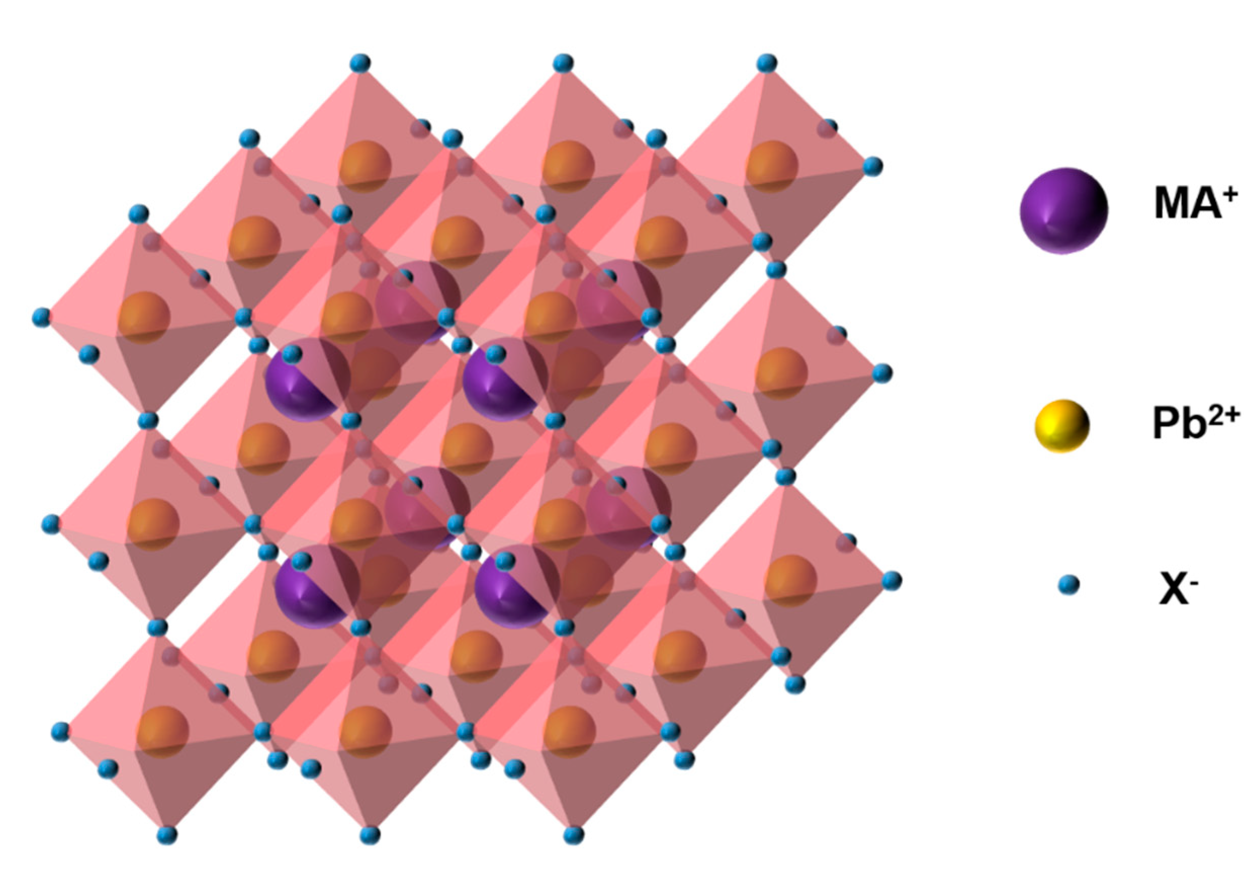
2. PSCs
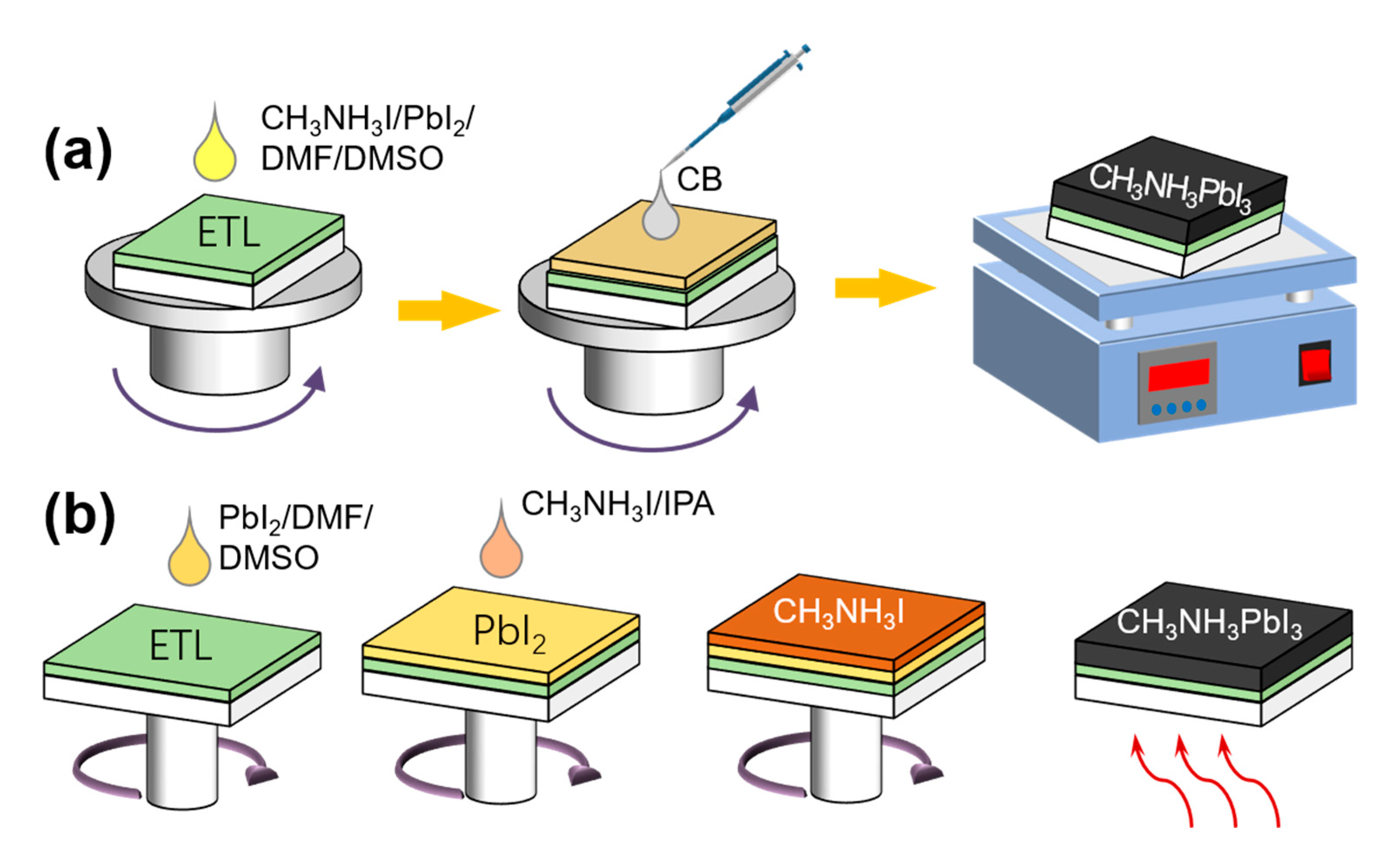
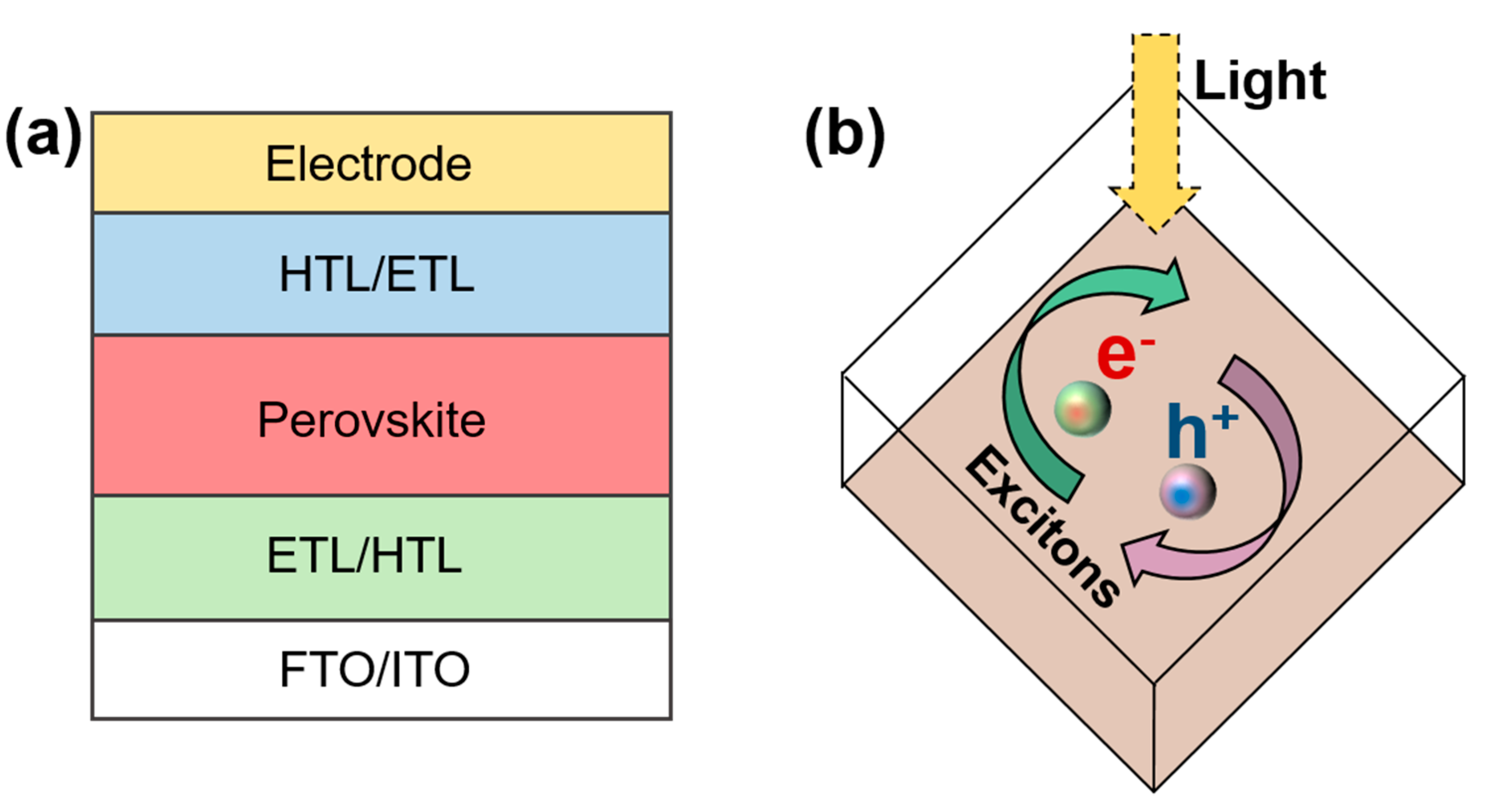
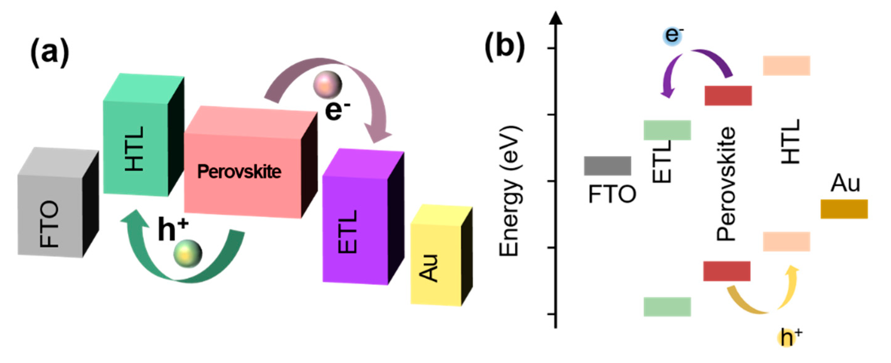
Structure and Principle of PSC
3. PSC Interface
3.1. Interfacial Band Arrangement of PSCs
3.2. Defects at Interface
3.3. Chemical Reaction at Interface
4. Interface Modification
4.1. Organic Material
4.1.1. Organic Salt
4.1.2. Graded Perovskite

| Passivation Materials | Perovskite | Jsc (mA·cm−2) | Voc (V) | FF (%) | PCE (%) | Year | Ref. |
|---|---|---|---|---|---|---|---|
| tBBAI | Cs0.05FA0.85MA0.10Pb(I0.97Br0.03)3 | 25.10 | 1.142 | 82.1 | 23.5 | 2020 | [56] |
| PEAI | Cs0.05FA0.85MA0.10Pb(I0.97Br0.03)3 | 25.01 | 1.122 | 80.9 | 22.7 | 2020 | [56] |
| EAI | FA0.9Cs0.07MA0.03Pb(I0.92Br0.08)3 | 24.36 | 1.123 | 80.4 | 22.30 | 2019 | [78] |
| IAI | FA0.9Cs0.07MA0.03Pb(I0.92Br0.08)3 | 24.14 | 1.103 | 79.4 | 21.60 | 2019 | [78] |
| GuaI | FA0.9Cs0.07MA0.03Pb(I0.92Br0.08)3 | 24.45 | 1.106 | 75.3 | 20.9 | 2019 | [78] |
| PEAI | (FAPbI3)1−x(MAPbBr3)x | 25.2 | 1.180 | 78.4 | 23.2 | 2019 | [79] |
| HTAB | (FAPbI3)0.95(MAPbBr3)0.05 | 24.88 | 1.152 | 81.4 | 23.3 | 2019 | [80] |
| NMAI | Cs0.05(MA0.15FA0.85)0.95Pb(I0.85Br0.15)3 | 22.28 | 1.174 | 77.63 | 20.57 | 2020 | [87] |
| oFPEAI | Cs0.05FA0.79MA0.16PbI2.49Br0.51 | 22.62 | 1.17 | 77.9 | 20.60 | 2020 | [88] |
| mFPEAI | Cs0.05FA0.79MA0.16PbI2.49Br0.51 | 22.75 | 1.175 | 76.8 | 20.52 | 2020 | [88] |
| pFPEAI | Cs0.05FA0.79MA0.16PbI2.49Br0.51 | 22.23 | 1.153 | 79.5 | 20.37 | 2020 | [88] |
| NMABr | CsFAMAPb(I)3 | 23.62 | 1.13 | 79.0 | 21.09 | 2020 | [89] |
| SBLC | MAPbI3 | 22.36 | 1.19 | 75.7 | 20.14 | 2020 | [90] |
| C4Br | (FAPbI3)0.92(MAPbBr3)0.08 | 24.5 | 1.15 | 81 | 23.2 | 2019 | [91] |
| C6Br | (FAPbI3)0.92(MAPbBr3)0.08 | 24.6 | 1.16 | 81.4 | 23.2 | 2019 | [91] |
| C8Br | (FAPbI3)0.92(MAPbBr3)0.08 | 24.5 | 1.16 | 82.0 | 23.3 | 2019 | [91] |
| PEAI | FASnI3 | 19.45 | 0.37 | 70.10 | 4.89 | 2018 | [92] |
| PZPY | Cs0.04MA0.16FA0.8PbI0.85Br0.15 | 21.70 | 1.08 | 77.0 | 18.10 | 2018 | [93] |
| PAI | CsFAMAPb(IBr)3 | 23.69 | 1.11 | 80.76 | 21.19 | 2020 | [94] |
| CsPbI2Br nanosheet–CsPbI2Br quantum dots | CsPbBrI2 | 12.93 | 1.19 | 0.80 | 12.39 | 2018 | [95] |
4.1.3. Chemical Passivation
4.2. Inorganic Material
4.2.1. Quantum Dots
4.2.2. Carbon Material
4.2.3. Oxide
5. Conclusions and Outlook
Author Contributions
Funding
Institutional Review Board Statement
Informed Consent Statement
Data Availability Statement
Conflicts of Interest
Abbreviation
| 0-D | zero-dimensional |
| 1-D | one-dimensional |
| 2-MP | 2-mercaptopyridine |
| 2-D | two-dimensional |
| 3-D | three-dimensional |
| APTES | (3-Aminopropyl) triethoxysilane |
| Cs | Cesium |
| C4Br | n-butylammonium bromide |
| C6Br | n-hexylammonium bromide |
| C8Br | n-octylammonium bromide |
| DPP-DTT | poly(N-alkyldiketopyrrolopyrrole dithienylthieno[3,2-b]thio-phene) |
| D4TBP | D-4-tert-butylphenylalanine |
| ETL | electron transporting layer |
| ETM | electron transporting material |
| FTO | fluorine-doped tin oxide |
| FA | Formamidinium |
| FAI | Formamidinium iodide |
| FF | fill factor |
| GO | graphene oxide |
| HTM | hole transport material |
| HTL | hole transporting layer |
| HTAB | n-hexyl trimethyl ammonium bromide |
| MA | methylammonium |
| MPTES | (3-mercaptopropyl) triethoxysilane |
| mFPEAI | 2-(3-fluorophenyl)ethylamine iodide |
| NMABr | 1-naphthylmethylammonium bromide |
| NERL | National renewable energy laboratory |
| oFPEAI | 2-(2-fluorophenyl)ethylamineiodide |
| OS | oligomeric SiO2 |
| pFPEAI | 2-(4-fluorophenyl)ethylamine iodide |
| PZPY | 2-(1H-pyrazol-1-yl)pyridine |
| PCBM | [6,6]-phenyl-C61-butyric acid methyl ester |
| PSCs | perovskite solar cells |
| PCE | power conversion efficiency |
| Py | pyridine |
| PTT | p-toluenethiol |
| PA | phenylpropionic acid |
| PAI | propargylammonium iodide |
| PEA | phenethylamine |
| PAA | Phenylalanine |
| PMMA | Polymethyl methacrylate polymer |
| P3HT | poly-(3-thiopheneaceticacid) |
| PEAI | phenylethylammonium iodide |
| PZPY | 3-(2-pyridyl)-pyrazol-1-yl |
| PEA | phenylethylammonium |
| PEI | poly(ethyleneimine) |
| Pd | Plumbum |
| Rb | Rubidium |
| Sn | Stannum |
| SBLC | S-benzyl-lcysteine |
| spiro-OMeTAD | 2,2′,7,7′-tetrakis-(N,N-di-p-methoxyphenylamine)9,9′-spirobifluorene |
| TBPO | tribenzylphosphine oxide |
| TPPO | triphenylphosphine oxide |
| TEOS | Tetraethyl orthosilicate |
| VA | Valine |
References
- Wu, Y.; Chen, W.; Chen, G.; Liu, L.; He, Z.; Liu, R. The Impact of Hybrid Compositional Film/Structure on Organic(-)Inorganic Perovskite Solar Cells. Nanomaterials 2018, 8, 356. [Google Scholar] [CrossRef]
- Da, P.; Zheng, G. Tailoring interface of lead-halide perovskite solar cells. Nano Res. 2017, 10, 1471–1497. [Google Scholar] [CrossRef]
- Li, Y.; Ji, L.; Liu, R.; Zhang, C.; Mak, C.H.; Zou, X.; Shen, H.-H.; Leu, S.-Y.; Hsu, H.-Y. A review on morphology engineering for highly efficient and stable hybrid perovskite solar cells. J. Mater. Chem. A 2018, 6, 12842–12875. [Google Scholar] [CrossRef]
- Wang, S.; Sakurai, T.; Wen, W.; Qi, Y. Energy Level Alignment at Interfaces in Metal Halide Perovskite Solar Cells. Adv. Mater. Interfaces 2018, 5, 1800260. [Google Scholar] [CrossRef]
- Du, P.; Gao, L.; Tang, J. Focus on performance of perovskite light-emitting diodes. Front. Optoelectron. 2020, 13, 235–245. [Google Scholar] [CrossRef]
- Liu, D.; Yu, B.-B.; Liao, M.; Jin, Z.; Zhou, L.; Zhang, X.; Wang, F.; He, H.; Gatti, T.; He, Z. Self-Powered and Broadband Lead-Free Inorganic Perovskite Photodetector with High Stability. Acs Appl. Mater. Interfaces 2020, 12, 30530–30537. [Google Scholar] [CrossRef]
- Xiao, X.; Hu, J.; Tang, S.; Yan, K.; Gao, B.; Chen, H.; Zou, D. Recent Advances in Halide Perovskite Memristors: Materials, Structures, Mechanisms, and Applications. Adv. Mater. Technol. 2020, 5, 1900914. [Google Scholar] [CrossRef]
- Nur’aini, A.; Oh, I. Volatile organic compound gas sensors based on methylammonium lead iodide perovskite operating at room temperature. Rsc Adv. 2020, 10, 12982–12987. [Google Scholar] [CrossRef]
- Yılmaz, B.; Yıldırım, R. Critical review of machine learning applications in perovskite solar research. Nano Energy 2021, 80, 105546. [Google Scholar] [CrossRef]
- Luo, D.; Su, R.; Zhang, W.; Gong, Q.; Zhu, R. Minimizing non-radiative recombination losses in perovskite solar cells. Nat. Rev. Mater. 2020, 5, 44–60. [Google Scholar] [CrossRef]
- NREL. 2021. Available online: https://pvdpc.nrel.gov/ (accessed on 21 February 2021).
- Jeong, M.; Choi, I.W.; Go, E.M.; Cho, Y.; Kim, M.; Lee, B.; Jeong, S.; Jo, Y.; Choi, H.W.; Lee, J.; et al. Stable perovskite solar cells with efficiency exceeding 24.8% and 0.3-V voltage loss. Science 2020, 369, 1615–1620. [Google Scholar] [CrossRef]
- Yang, Z.; Babu, B.H.; Wu, S.; Liu, T.; Fang, S.; Xiong, Z.; Han, L.; Chen, W. Review on Practical Interface Engineering of Perovskite Solar Cells: From Efficiency to Stability. Sol. RRL 2020, 4, 1900257. [Google Scholar] [CrossRef]
- Choi, H.; Choi, K.; Choi, Y.; Kim, T.; Lim, S.; Park, T. A Review on Reducing Grain Boundaries and Morphological Improvement of Perovskite Solar Cells from Methodology and Material-Based Perspectives. Small Methods 2020, 4, 1900569. [Google Scholar] [CrossRef]
- Roy, P.; Kumar Sinha, N.; Tiwari, S.; Khare, A. A review on perovskite solar cells: Evolution of architecture, fabrication techniques, commercialization issues and status. Sol. Energy 2020, 198, 665–688. [Google Scholar] [CrossRef]
- Gao, W.; Chen, C.; Ran, C.; Zheng, H.; Dong, H.; Xia, Y.; Chen, Y.; Huang, W. A-Site Cation Engineering of Metal Halide Perovskites: Version 3.0 of Efficient Tin-Based Lead-Free Perovskite Solar Cells. Adv. Funct. Mater. 2020, 30, 2000794. [Google Scholar] [CrossRef]
- Parida, B.; Yoon, S.; Jeong, S.M.; Cho, J.S.; Kim, J.-K.; Kang, D.-W. Recent progress on cesium lead/tin halide-based inorganic perovskites for stable and efficient solar cells: A review. Sol. Energy Mater. Sol. Cells 2020, 204, 110212. [Google Scholar] [CrossRef]
- Abdel-Shakour, M.; Chowdhury, T.H.; Matsuishi, K.; Bedja, I.; Moritomo, Y.; Islam, A. High-Efficiency Tin Halide Perovskite Solar Cells: The Chemistry of Tin (II) Compounds and Their Interaction with Lewis Base Additives during Perovskite Film Formation. Sol. RRL 2021, 5, 2000606. [Google Scholar] [CrossRef]
- Nie, R.; Sumukam, R.R.; Reddy, S.H.; Banavoth, M.; Seok, S.I. Lead-free perovskite solar cells enabled by hetero-valent substitutes. Energy Environ. Sci. 2020, 13, 2363–2385. [Google Scholar] [CrossRef]
- Laamari, M.E.; Cheknane, A.; Benghia, A.; Hilal, H.S. Optimized opto-electronic and mechanical properties of orthorhombic methylamunium lead halides (MAPbX3) (X = I, Br and Cl) for photovoltaic applications. Sol. Energy 2019, 182, 9–15. [Google Scholar] [CrossRef]
- Suarez, B.; Gonzalez-Pedro, V.; Ripolles, T.S.; Sanchez, R.S.; Otero, L.; Mora-Sero, I. Recombination Study of Combined Halides (Cl, Br, I) Perovskite Solar Cells. J. Phys. Chem. Lett. 2014, 5, 1628–1635. [Google Scholar] [CrossRef]
- Li, X.; He, B.; Gong, Z.; Zhu, J.; Zhang, W.; Chen, H.; Duan, Y.; Tang, Q. Compositional Engineering of Chloride Ion-Doped CsPbBr3 Halides for Highly Efficient and Stable All-Inorganic Perovskite Solar Cells. Sol. RRL 2020, 4, 2000362. [Google Scholar] [CrossRef]
- Al-Asbahi, B.A.; Qaid, S.M.H.; Hezam, M.; Bedja, I.; Ghaithan, H.M.; Aldwayyan, A.S. Effect of deposition method on the structural and optical properties of CH3NH3PbI3 perovskite thin films. Opt. Mater. 2020, 103, 109836. [Google Scholar] [CrossRef]
- Li, M.; Xie, Y.-M.; Xu, X.; Huo, Y.; Tsang, S.-W.; Yang, Q.-D.; Cheng, Y. Comparison of processing windows and electronic properties between CH3NH3PbI3 perovskite fabricated by one-step and two-step solution processes. Org. Electron. 2018, 63, 159–165. [Google Scholar] [CrossRef]
- Xiao, M.; Huang, F.; Huang, W.; Dkhissi, Y.; Zhu, Y.; Etheridge, J.; Gray-Weale, A.; Bach, U.; Cheng, Y.-B.; Spiccia, L. A Fast Deposition-Crystallization Procedure for Highly Efficient Lead Iodide Perovskite Thin-Film Solar Cells. Angew. Chem. Int. Ed. 2014, 53, 9898–9903. [Google Scholar] [CrossRef]
- Angmo, D.; DeLuca, G.; Scully, A.D.; Chesman, A.S.R.; Seeber, A.; Zuo, C.; Vak, D.; Bach, U.; Gao, M. A Lab-to-Fab Study toward Roll-to-Roll Fabrication of Reproducible Perovskite Solar Cells under Ambient Room Conditions. Cell Rep. Phys. Sci. 2021, 100293. [Google Scholar] [CrossRef]
- Soto-Montero, T.; Soltanpoor, W.; Morales-Masis, M. Pressing challenges of halide perovskite thin film growth. Appl. Mater. 2020, 8, 110903. [Google Scholar] [CrossRef]
- Chen, J.; Park, N.-G. Materials and Methods for Interface Engineering toward Stable and Efficient Perovskite Solar Cells. ACS Energy Lett. 2020, 5, 2742–2786. [Google Scholar] [CrossRef]
- Izadi, F.; Ghobadi, A.; Gharaati, A.; Minbashi, M.; Hajjiah, A. Effect of interface defects on high efficient perovskite solar cells. Optik 2021, 227, 166061. [Google Scholar] [CrossRef]
- Meng, L.; You, J.; Guo, T.-F.; Yang, Y. Recent Advances in the Inverted Planar Structure of Perovskite Solar Cells. Acc. Chem. Res. 2016, 49, 155–165. [Google Scholar] [CrossRef]
- Kumar, N.; Rani, J.; Kurchania, R. A review on power conversion efficiency of lead iodide perovskite-based solar cells. Mater. Today Proc. 2020. [Google Scholar] [CrossRef]
- Li, H.; Li, F.; Shen, Z.; Han, S.-T.; Chen, J.; Dong, C.; Chen, C.; Zhou, Y.; Wang, M. Photoferroelectric perovskite solar cells: Principles, advances and insights. Nano Today 2021, 37, 101062. [Google Scholar] [CrossRef]
- Petrus, M.L.; Schlipf, J.; Li, C.; Gujar, T.P.; Giesbrecht, N.; Müller-Buschbaum, P.; Thelakkat, M.; Bein, T.; Hüttner, S.; Docampo, P. Capturing the Sun: A Review of the Challenges and Perspectives of Perovskite Solar Cells. Adv. Energy Mater. 2017, 7, 1700264. [Google Scholar] [CrossRef]
- Choi, K.; Choi, H.; Min, J.; Kim, T.; Kim, D.; Son, S.Y.; Kim, G.-W.; Choi, J.; Park, T. A Short Review on Interface Engineering of Perovskite Solar Cells: A Self-Assembled Monolayer and Its Roles. Sol. RRL 2020, 4, 1900251. [Google Scholar] [CrossRef]
- Shi, J.; Xu, X.; Li, D.; Meng, Q. Interfaces in Perovskite Solar Cells. Small 2015, 11, 2472–2486. [Google Scholar] [CrossRef]
- Yang, X.; Luo, D.; Xiang, Y.; Zhao, L.; Anaya, M.; Shen, Y.; Wu, J.; Yang, W.; Chiang, Y.-H.; Tu, Y.; et al. Buried Interfaces in Halide Perovskite Photovoltaics. Adv. Mater. 2021, 2006435. [Google Scholar] [CrossRef]
- Matteocci, F.; Busby, Y.; Pireaux, J.-J.; Divitini, G.; Cacovich, S.; Ducati, C.; Di Carlo, A. Interface and Composition Analysis on Perovskite Solar Cells. Acs Appl. Mater. Interfaces 2015, 7, 26176–26183. [Google Scholar] [CrossRef] [PubMed]
- Feng, W.; Geng, R.; Liu, D.; Wang, T.; Testoff, T.T.; Li, W.; Hu, W.; Wang, L.; Zhou, X. A charge-separated interfacial hole transport semiconductor for efficient and stable perovskite solar cells. Org. Electron. 2021, 88, 105988. [Google Scholar] [CrossRef]
- Jin, Z.; Yu, B.-B.; Liao, M.; Liu, D.; Xiu, J.; Zhang, Z.; Lifshitz, E.; Tang, J.; Song, H.; He, Z. Enhanced efficiency and stability in Sn-based perovskite solar cells with secondary crystallization growth. J. Energy Chem. 2021, 54, 414–421. [Google Scholar] [CrossRef]
- Kim, J.Y.; Lee, J.-W.; Jung, H.S.; Shin, H.; Park, N.-G. High-Efficiency Perovskite Solar Cells. Chem. Rev. 2020, 120, 7867–7918. [Google Scholar] [CrossRef]
- Wang, M.; Lei, Y.; Xu, Y.; Han, L.; Ci, Z.; Jin, Z. The J–V Hysteresis Behavior and Solutions in Perovskite Solar Cells. Sol. RRL 2020, 4, 2000586. [Google Scholar] [CrossRef]
- Kumar, A.; Rana, A.; Vashistha, N.; Garg, K.K.; Singh, R.K. Defect states influencing hysteresis and performance of perovskite solar cells. Sol. Energy 2020, 211, 345–353. [Google Scholar] [CrossRef]
- Wang, D.; Li, W.; Sun, W.; Liu, X.; Li, G.; Wu, Z.; Wu, J.; Lan, Z. Guanidinium iodide modification enabled highly efficient and stable all-inorganic CsPbBr3 perovskite solar cells. Electrochim. Acta 2021, 365, 137360. [Google Scholar] [CrossRef]
- Mansfeldova, V.; Zlamalova, M.; Tarabkova, H.; Janda, P.; Vorokhta, M.; Piliai, L.; Kavan, L. Work Function of TiO2 (Anatase, Rutile, and Brookite) Single Crystals: Effects of the Environment. J. Phys. Chem. C 2021, 125, 1902–1912. [Google Scholar] [CrossRef]
- Ishii, H.; Sugiyama, K.; Ito, E.; Seki, K. Energy Level Alignment and Interfacial Electronic Structures at Organic/Metal and Organic/Organic Interfaces. Adv. Mater. 1999, 11, 605–625. [Google Scholar] [CrossRef]
- Wang, C.; Moro, F.; Ni, S.; Zhang, Q.; Pan, G.; Yang, J.; Zhang, F.; Buyanova, I.A.; Chen, W.M.; Liu, X.; et al. Thermal-annealing effects on energy level alignment at organic heterojunctions and corresponding voltage losses in all-polymer solar cells. Nano Energy 2020, 72, 104677. [Google Scholar] [CrossRef]
- Li, N.; Niu, X.; Pei, F.; Liu, H.; Cao, Y.; Liu, Y.; Xie, H.; Gao, Y.; Chen, Q.; Mo, F.; et al. Energy-Level Modulation in Diboron-Modified SnO2 for High-Efficiency Perovskite Solar Cells. Sol. RRL 2020, 4, 1900217. [Google Scholar] [CrossRef]
- Xie, L.; Cao, Z.; Wang, J.; Wang, A.; Wang, S.; Cui, Y.; Xiang, Y.; Niu, X.; Hao, F.; Ding, L. Improving energy level alignment by adenine for efficient and stable perovskite solar cells. Nano Energy 2020, 74, 104846. [Google Scholar] [CrossRef]
- Zhao, P.; Kim, B.J.; Jung, H.S. Passivation in perovskite solar cells: A review. Mater. Today Energy 2018, 7, 267–286. [Google Scholar] [CrossRef]
- Chen, K.; Wu, J.; Wang, Y.; Guo, Q.; Chen, Q.; Cao, T.; Guo, X.; Zhou, Y.; Chen, N.; Zhang, M.; et al. Defect passivation by alcohol-soluble small molecules for efficient p–i–n planar perovskite solar cells with high open-circuit voltage. J. Mater. Chem. A 2019, 7, 21140–21148. [Google Scholar] [CrossRef]
- Kim, J.; Ho-Baillie, A.; Huang, S. Review of Novel Passivation Techniques for Efficient and Stable Perovskite Solar Cells. Sol. RRL 2019, 3, 1800302. [Google Scholar] [CrossRef]
- Noël, C.; Pescetelli, S.; Agresti, A.; Franquet, A.; Spampinato, V.; Felten, A.; di Carlo, A.; Houssiau, L.; Busby, Y. Hybrid Perovskites Depth Profiling with Variable-Size Argon Clusters and Monatomic Ions Beams. Materials 2019, 12, 726. [Google Scholar] [CrossRef]
- Yang, D.; Yang, R.; Priya, S.; Liu, S. Recent Advances in Flexible Perovskite Solar Cells: Fabrication and Applications. Angew. Chem. Int. Ed. 2019, 58, 4466–4483. [Google Scholar] [CrossRef]
- Liu, D.; Kelly, T.L. Perovskite solar cells with a planar heterojunction structure prepared using room-temperature solution processing techniques. Nat. Photonics 2014, 8, 133–138. [Google Scholar] [CrossRef]
- Wang, Y.; Zhang, T.; Xu, F.; Li, Y.; Zhao, Y. A Facile Low Temperature Fabrication of High Performance CsPbI2Br All-Inorganic Perovskite Solar Cells. Sol. RRL 2018, 2, 1700180. [Google Scholar] [CrossRef]
- Zhu, H.; Liu, Y.; Eickemeyer, F.T.; Pan, L.; Ren, D.; Ruiz-Preciado, M.A.; Carlsen, B.; Yang, B.; Dong, X.; Wang, Z.; et al. Tailored Amphiphilic Molecular Mitigators for Stable Perovskite Solar Cells with 23.5% Efficiency. Adv. Mater. 2020, 32, 1907757. [Google Scholar] [CrossRef]
- Wu, Y.; Chen, W.; Lin, Y.; Tu, B.; Lan, X.; Wu, Z.; Liu, R.; Djurišić, A.B.; He, Z.B. General Method to Define the Type of Carrier Transport Materials for Perovskite Solar Cells via Kelvin Probes Microscopy. Acs Appl. Energy Mater. 2018, 1, 3984–3991. [Google Scholar] [CrossRef]
- Hsu, H.-L.; Jiang, B.-H.; Lan, J.-M.; Wu, C.-H.; Jeng, R.-J.; Chen, C.-P. Small Molecules with Controllable Molecular Weights Passivate Surface Defects in Air-Stable p-i-n Perovskite Solar Cells. Adv. Electron. Mater. 2021, 7, 2000870. [Google Scholar] [CrossRef]
- Li, Y.; Wu, H.; Qi, W.; Zhou, X.; Li, J.; Cheng, J.; Zhao, Y.; Li, Y.; Zhang, X. Passivation of defects in perovskite solar cell: From a chemistry point of view. Nano Energy 2020, 77, 105237. [Google Scholar] [CrossRef]
- Zhang, Z.; Wu, J.; Li, S.; Liu, S.; Wang, Q.; Mei, A.; Rong, Y.; Han, H.; Hu, Y. Progress in Multifunctional Molecules for Perovskite Solar Cells. Sol. RRL 2020, 4, 1900248. [Google Scholar] [CrossRef]
- Yang, S.; Dai, J.; Yu, Z.; Shao, Y.; Zhou, Y.; Xiao, X.; Zeng, X.C.; Huang, J. Tailoring Passivation Molecular Structures for Extremely Small Open-Circuit Voltage Loss in Perovskite Solar Cells. J. Am. Chem. Soc. 2019, 141, 5781–5787. [Google Scholar] [CrossRef]
- Hamill, J.C.; Romiluyi, O.; Thomas, S.A.; Cetola, J.; Schwartz, J.; Toney, M.F.; Clancy, P.; Loo, Y.-L. Sulfur-Donor Solvents Strongly Coordinate Pb2+ in Hybrid Organic–Inorganic Perovskite Precursor Solutions. J. Phys. Chem. C 2020, 124, 14496–14502. [Google Scholar] [CrossRef]
- Chen, W.; Gan, Z.; Green, M.A.; Jia, B.; Wen, X. Revealing Dynamic Effects of Mobile Ions in Halide Perovskite Solar Cells Using Time-Resolved Microspectroscopy. Small Methods 2021, 5, 2000731. [Google Scholar] [CrossRef]
- Meggiolaro, D.; Mosconi, E.; De Angelis, F. Formation of Surface Defects Dominates Ion Migration in Lead-Halide Perovskites. ACS Energy Lett. 2019, 4, 779–785. [Google Scholar] [CrossRef]
- Tong, C.-J.; Li, L.; Liu, L.-M.; Prezhdo, O.V. Synergy between Ion Migration and Charge Carrier Recombination in Metal-Halide Perovskites. J. Am. Chem. Soc. 2020, 142, 3060–3068. [Google Scholar] [CrossRef] [PubMed]
- Das, U.; Das, D.; Paul, B.; Rabha, T.; Pattanayak, S.; Kanjilal, A.; Bhattacharjee, S.; Sarkar, P.; Roy, A. Induced Vacancy-Assisted Filamentary Resistive Switching Device Based on RbPbI3–xClx Perovskite for RRAM Application. Acs Appl. Mater. Interfaces 2020, 12, 41718–41727. [Google Scholar] [CrossRef] [PubMed]
- Wang, J.; Zhang, J.; Zhou, Y.; Liu, H.; Xue, Q.; Li, X.; Chueh, C.-C.; Yip, H.-L.; Zhu, Z.; Jen, A.K.Y. Highly efficient all-inorganic perovskite solar cells with suppressed non-radiative recombination by a Lewis base. Nat. Commun. 2020, 11, 177. [Google Scholar] [CrossRef] [PubMed]
- Xu, J.; Liang, L.; Mai, C.-L.; Zhang, Z.; Zhou, Q.; Xiong, Q.; Zhang, Z.; Deng, L.; Gao, P. Lewis-base containing spiro type hole transporting materials for high-performance perovskite solar cells with efficiency approaching 20%. Nanoscale 2020, 12, 13157–13164. [Google Scholar] [CrossRef]
- Chen, B.; Baek, S.-W.; Hou, Y.; Aydin, E.; De Bastiani, M.; Scheffel, B.; Proppe, A.; Huang, Z.; Wei, M.; Wang, Y.-K.; et al. Enhanced optical path and electron diffusion length enable high-efficiency perovskite tandems. Nat. Commun. 2020, 11, 1257. [Google Scholar] [CrossRef]
- Motavassel, S.; Seifouri, M.; Olyaee, S. Efficiency improvement of perovskite solar cell by modifying structural parameters and using Ag nanoparticles. Appl. Phys. A 2021, 127, 96. [Google Scholar] [CrossRef]
- Ball, J.M.; Petrozza, A. Defects in perovskite-halides and their effects in solar cells. Nat. Energy 2016, 1, 16149. [Google Scholar] [CrossRef]
- Ran, C.; Xu, J.; Gao, W.; Huang, C.; Dou, S. Defects in metal triiodide perovskite materials towards high-performance solar cells: Origin, impact, characterization, and engineering. Chem. Soc. Rev. 2018, 47, 4581–4610. [Google Scholar] [CrossRef]
- Ono, L.K.; Liu, S.; Qi, Y. Reducing Detrimental Defects for High-Performance Metal Halide Perovskite Solar Cells. Angew. Chem. Int. Ed. 2020, 59, 6676–6698. [Google Scholar] [CrossRef]
- Yun, S.-C.; Ma, S.; Kwon, H.-C.; Kim, K.; Jang, G.; Yang, H.; Moon, J. Amino acid salt-driven planar hybrid perovskite solar cells with enhanced humidity stability. Nano Energy 2019, 59, 481–491. [Google Scholar] [CrossRef]
- Sun, C.; Xu, L.; Lai, X.; Li, Z.; He, M. Advanced Strategies of Passivating Perovskite Defects for High-Performance Solar Cells. Energy Environ. Mater. 2020, 1–10. [Google Scholar] [CrossRef]
- Li, Z.; Wang, F.; Liu, C.; Gao, F.; Shen, L.; Guo, W. Efficient perovskite solar cells enabled by ion-modulated grain boundary passivation with a fill factor exceeding 84%. J. Mater. Chem. A 2019, 7, 22359–22365. [Google Scholar] [CrossRef]
- Hou, M.; Xu, Y.; Zhou, B.; Tian, Y.; Wu, Y.; Zhang, D.; Wang, G.; Li, B.; Ren, H.; Li, Y.; et al. Aryl Diammonium Iodide Passivation for Efficient and Stable Hybrid Organ-Inorganic Perovskite Solar Cells. Adv. Funct. Mater. 2020, 30, 2002366. [Google Scholar] [CrossRef]
- Alharbi, E.A.; Alyamani, A.Y.; Kubicki, D.J.; Uhl, A.R.; Walder, B.J.; Alanazi, A.Q.; Luo, J.; Burgos-Caminal, A.; Albadri, A.; Albrithen, H.; et al. Atomic-level passivation mechanism of ammonium salts enabling highly efficient perovskite solar cells. Nat. Commun. 2019, 10, 3008. [Google Scholar] [CrossRef]
- Jiang, Q.; Zhao, Y.; Zhang, X.; Yang, X.; Chen, Y.; Chu, Z.; Ye, Q.; Li, X.; Yin, Z.; You, J. Surface passivation of perovskite film for efficient solar cells. Nat. Photonics 2019, 13, 460–466. [Google Scholar] [CrossRef]
- Jung, E.H.; Jeon, N.J.; Park, E.Y.; Moon, C.S.; Shin, T.J.; Yang, T.Y.; Noh, J.H.; Seo, J. Efficient, stable and scalable perovskite solar cells using poly(3-hexylthiophene). Nature 2019, 567, 511–515. [Google Scholar] [CrossRef] [PubMed]
- Krishna, A.; Gottis, S.; Nazeeruddin, M.K.; Sauvage, F. Mixed Dimensional 2D/3D Hybrid Perovskite Absorbers: The Future of Perovskite Solar Cells? Adv. Funct. Mater. 2019, 29, 1806482. [Google Scholar] [CrossRef]
- Kim, H.; Kim, J.S.; Heo, J.-M.; Pei, M.; Park, I.-H.; Liu, Z.; Yun, H.J.; Park, M.-H.; Jeong, S.-H.; Kim, Y.-H.; et al. Proton-transfer-induced 3D/2D hybrid perovskites suppress ion migration and reduce luminance overshoot. Nat. Commun. 2020, 11, 3378. [Google Scholar] [CrossRef]
- Yao, D.; Mao, X.; Wang, X.; Yang, Y.; Hoang, M.T.; Du, A.; Waclawik, E.R.; Wilson, G.J.; Wang, H. The effect of ethylene-amine ligands enhancing performance and stability of perovskite solar cells. J. Power Sources 2020, 463, 228210. [Google Scholar] [CrossRef]
- Guo, P.; Ye, Q.; Yang, X.; Zhang, J.; Xu, F.; Shchukin, D.; Wei, B.; Wang, H. Surface & grain boundary co-passivation by fluorocarbon based bifunctional molecules for perovskite solar cells with efficiency over 21%. J. Mater. Chem. A 2019, 7, 2497–2506. [Google Scholar] [CrossRef]
- Jiang, X.; Chen, S.; Li, Y.; Zhang, L.; Shen, N.; Zhang, G.; Du, J.; Fu, N.; Xu, B. Direct Surface Passivation of Perovskite Film by 4-Fluorophenethylammonium Iodide toward Stable and Efficient Perovskite Solar Cells. Acs Appl. Mater. Inter. 2021, 13, 2558–2565. [Google Scholar] [CrossRef] [PubMed]
- Urbina, A. The balance between efficiency, stability and environmental impacts in perovskite solar cells: A review. J. Phys. Energy 2020, 2, 022001. [Google Scholar] [CrossRef]
- Liang, L.; Luo, H.; Hu, J.; Li, H.; Gao, P. Efficient Perovskite Solar Cells by Reducing Interface-Mediated Recombination: A Bulky Amine Approach. Adv. Energy Mater. 2020, 10, 2000197. [Google Scholar] [CrossRef]
- Zhou, Q.; Xiong, Q.; Zhang, Z.; Hu, J.; Lin, F.; Liang, L.; Wu, T.; Wang, X.; Wu, J.; Zhang, B.; et al. Fluoroaromatic Cation-Assisted Planar Junction Perovskite Solar Cells with Improved VOC and Stability: The Role of Fluorination Position. Sol. RRL 2020, 4, 2000107. [Google Scholar] [CrossRef]
- Zhao, S.; Qin, M.; Wang, H.; Xie, J.; Xie, F.; Chen, J.; Lu, X.; Yan, K.; Xu, J. Cascade Type-II 2D/3D Perovskite Heterojunctions for Enhanced Stability and Photovoltaic Efficiency. Sol. RRL 2020, 4, 2000282. [Google Scholar] [CrossRef]
- Hu, J.; Wang, C.; Qiu, S.; Zhao, Y.; Gu, E.; Zeng, L.; Yang, Y.; Li, C.; Liu, X.; Forberich, K.; et al. Spontaneously Self-Assembly of a 2D/3D Heterostructure Enhances the Efficiency and Stability in Printed Perovskite Solar Cells. Adv. Energy Mater. 2020, 10, 2000173. [Google Scholar] [CrossRef]
- Yoo, J.J.; Wieghold, S.; Sponseller, M.C.; Chua, M.R.; Bertram, S.N.; Hartono, N.T.P.; Tresback, J.S.; Hansen, E.C.; Correa-Baena, J.-P.; Bulović, V.; et al. An interface stabilized perovskite solar cell with high stabilized efficiency and low voltage loss. Energy Environ. Sci. 2019, 12, 2192–2199. [Google Scholar] [CrossRef]
- Ran, C.; Xi, J.; Gao, W.; Yuan, F.; Lei, T.; Jiao, B.; Hou, X.; Wu, Z. Bilateral Interface Engineering toward Efficient 2D–3D Bulk Heterojunction Tin Halide Lead-Free Perovskite Solar Cells. Acs Energy Lett. 2018, 3, 713–721. [Google Scholar] [CrossRef]
- Fan, J.; Ma, Y.; Zhang, C.; Liu, C.; Li, W.; Schropp, R.E.I.; Mai, Y. Thermodynamically Self-Healing 1D–3D Hybrid Perovskite Solar Cells. Adv. Energy Mater. 2018, 1703421. [Google Scholar] [CrossRef]
- Yang, N.; Zhu, C.; Chen, Y.; Zai, H.; Wang, C.; Wang, X.; Wang, H.; Ma, S.; Gao, Z.; Wang, X.; et al. An in situ cross-linked 1D/3D perovskite heterostructure improves the stability of hybrid perovskite solar cells for over 3000 h operation. Energy Environ. Sci. 2020, 13, 4344–4352. [Google Scholar] [CrossRef]
- Zhang, J.; Bai, D.; Jin, Z.; Bian, H.; Wang, K.; Sun, J.; Wang, Q.; Liu, S. 3D–2D–0D Interface Profiling for Record Efficiency All-Inorganic CsPbBrI2 Perovskite Solar Cells with Superior Stability. Adv. Energy Mater. 2018, 1703246. [Google Scholar] [CrossRef]
- Yang, J.; Xiong, S.; Song, J.; Wu, H.; Zeng, Y.; Lu, L.; Shen, K.; Hao, T.; Ma, Z.; Liu, F.; et al. Energetics and Energy Loss in 2D Ruddlesden–Popper Perovskite Solar Cells. Adv. Energy Mater. 2020, 10, 2000687. [Google Scholar] [CrossRef]
- Davy, M.M.; Jadel, T.M.; Qin, C.; Luyun, B.; Mina, G. Recent progress in low dimensional (quasi-2D) and mixed dimensional (2D/3D) tin-based perovskite solar cells. Sustain. Energy Fuels 2021, 5, 34–51. [Google Scholar] [CrossRef]
- Mai, C.-L.; Zhou, Q.; Xiong, Q.; Chen, C.-C.; Xu, J.; Zhang, Z.; Lee, H.-W.; Yeh, C.-Y.; Gao, P. Donor–π–Acceptor Type Porphyrin Derivatives Assisted Defect Passivation for Efficient Hybrid Perovskite Solar Cells. Adv. Funct. Mater. 2020, 31, 2007762. [Google Scholar] [CrossRef]
- Akin, S.; Arora, N.; Zakeeruddin, S.M.; Grätzel, M.; Friend, R.H.; Dar, M.I. New Strategies for Defect Passivation in High-Efficiency Perovskite Solar Cells. Adv. Energy Mater. 2020, 10, 1903090. [Google Scholar] [CrossRef]
- Wang, K.; Liu, J.; Yin, J.; Aydin, E.; Harrison, G.T.; Liu, W.; Chen, S.; Mohammed, O.F.; De Wolf, S. Defect Passivation in Perovskite Solar Cells by Cyano-Based π-Conjugated Molecules for Improved Performance and Stability. Adv. Funct. Mater. 2020, 30, 2002861. [Google Scholar] [CrossRef]
- Azmi, R.; Nurrosyid, N.; Lee, S.-H.; Al Mubarok, M.; Lee, W.; Hwang, S.; Yin, W.; Ahn, T.K.; Kim, T.-W.; Ryu, D.Y.; et al. Shallow and Deep Trap State Passivation for Low-Temperature Processed Perovskite Solar Cells. Acs Energy Lett. 2020, 5, 1396–1403. [Google Scholar] [CrossRef]
- Luo, C.; Li, G.; Chen, L.; Dong, J.; Yu, M.; Xu, C.; Yao, Y.; Wang, M.; Song, Q.; Zhang, S. Passivation of defects in inverted perovskite solar cells using an imidazolium-based ionic liquid. Sustain. Energy Fuels 2020, 4, 3971–3978. [Google Scholar] [CrossRef]
- Chen, W.; Wang, Y.; Pang, G.; Koh, C.W.; Djurišić, A.B.; Wu, Y.; Tu, B.; Liu, F.-z.; Chen, R.; Woo, H.Y.; et al. Conjugated Polymer–Assisted Grain Boundary Passivation for Efficient Inverted Planar Perovskite Solar Cells. Adv. Funct. Mater. 2019, 29, 1808855. [Google Scholar] [CrossRef]
- Su, L.; Xiao, Y.; Lu, L.; Han, G.; Zhu, M. Enhanced stability and solar cell performance via π-conjugated Lewis base passivation of organic inorganic lead halide perovskites. Org. Electron. 2020, 77, 105519. [Google Scholar] [CrossRef]
- Shu, H.; Xia, J.; Yang, H.; Luo, J.; Wan, Z.; Malik, H.A.; Han, F.; Yao, X.; Jia, C. Self-Assembled Hydrophobic Molecule-Based Surface Modification: A Strategy to Improve Efficiency and Stability of Perovskite Solar Cells. ACS Sustain. Chem. Eng. 2020, 8, 10859–10869. [Google Scholar] [CrossRef]
- Dong, H.; Xi, J.; Zuo, L.; Li, J.; Yang, Y.; Wang, D.; Yu, Y.; Ma, L.; Ran, C.; Gao, W.; et al. Conjugated Molecules “Bridge”: Functional Ligand toward Highly Efficient and Long-Term Stable Perovskite Solar Cell. Adv. Funct. Mater. 2019, 29, 1808119. [Google Scholar] [CrossRef]
- Rana, P.J.S.; Gunasekaran, R.K.; Park, S.H.; Tamilavan, V.; Karuppanan, S.; Kim, H.-J.; Prabakar, K. Open Atmosphere-Processed Stable Perovskite Solar Cells Using Molecular Engineered, Dopant-Free, Highly Hydrophobic Polymeric Hole-Transporting Materials: Influence of Thiophene and Alkyl Chain on Power Conversion Efficiency. J. Phys. Chem. C 2019, 123, 8560–8568. [Google Scholar] [CrossRef]
- Wu, T.; Wang, Y.; Li, X.; Wu, Y.; Meng, X.; Cui, D.; Yang, X.; Han, L. Efficient Defect Passivation for Perovskite Solar Cells by Controlling the Electron Density Distribution of Donor-π-Acceptor Molecules. Adv. Energy Mater. 2019, 9, 1803766. [Google Scholar] [CrossRef]
- Li, H.; Shi, J.; Deng, J.; Chen, Z.; Li, Y.; Zhao, W.; Wu, J.; Wu, H.; Luo, Y.; Li, D.; et al. Intermolecular π–π Conjugation Self-Assembly to Stabilize Surface Passivation of Highly Efficient Perovskite Solar Cells. Adv. Mater. 2020, 32, 1907396. [Google Scholar] [CrossRef] [PubMed]
- Zhao, H.; Yang, S.; Han, Y.; Yuan, S.; Jiang, H.; Duan, C.; Liu, Z.; Liu, S. A High Mobility Conjugated Polymer Enables Air and Thermally Stable CsPbI2Br Perovskite Solar Cells with an Efficiency Exceeding 15%. Adv. Mater. Technol. 2019, 4, 1900311. [Google Scholar] [CrossRef]
- Hu, X.; Wang, H.; Wang, M.; Zang, Z. Interfacial defects passivation using fullerene-polymer mixing layer for planar-structure perovskite solar cells with negligible hysteresis. Sol. Energy 2020, 206, 816–825. [Google Scholar] [CrossRef]
- Ferdowsi, P.; Ochoa-Martinez, E.; Alonso, S.S.; Steiner, U.; Saliba, M. Ultrathin polymeric films for interfacial passivation in wide band-gap perovskite solar cells. Sci. Rep. 2020, 10, 22260. [Google Scholar] [CrossRef]
- Zhang, H.; Wu, Y.; Shen, C.; Li, E.; Yan, C.; Zhang, W.; Tian, H.; Han, L.; Zhu, W.-H. Efficient and Stable Chemical Passivation on Perovskite Surface via Bidentate Anchoring. Adv. Energy Mater. 2019, 9, 1803573. [Google Scholar] [CrossRef]
- Bett, A.J.; Schulze, P.S.C.; Winkler, K.M.; Kabakli, Ö.S.; Ketterer, I.; Mundt, L.E.; Reichmuth, S.K.; Siefer, G.; Cojocaru, L.; Tutsch, L.; et al. Two-terminal Perovskite silicon tandem solar cells with a high-Bandgap Perovskite absorber enabling voltages over 1.8 V. Prog. Photovolt. Res. Appl. 2020, 28, 99–110. [Google Scholar] [CrossRef]
- Zhong, Y.; Hufnagel, M.; Thelakkat, M.; Li, C.; Huettner, S. Role of PCBM in the Suppression of Hysteresis in Perovskite Solar Cells. Adv. Funct. Mater. 2020, 30, 1908920. [Google Scholar] [CrossRef]
- Aidarkhanov, D.; Ren, Z.; Lim, C.-K.; Yelzhanova, Z.; Nigmetova, G.; Taltanova, G.; Baptayev, B.; Liu, F.; Cheung, S.H.; Balanay, M.; et al. Passivation engineering for hysteresis-free mixed perovskite solar cells. Sol. Energy Mater. Sol. Cells 2020, 215, 110648. [Google Scholar] [CrossRef]
- Fang, Z.; Chen, W.; Shi, Y.; Zhao, J.; Chu, S.; Zhang, J.; Xiao, Z. Dual Passivation of Perovskite Defects for Light-Emitting Diodes with External Quantum Efficiency Exceeding 20%. Adv. Funct. Mater. 2020, 30, 1909754. [Google Scholar] [CrossRef]
- Qi, W.; Zhou, X.; Li, J.; Cheng, J.; Li, Y.; Ko, M.J.; Zhao, Y.; Zhang, X. Inorganic material passivation of defects toward efficient perovskite solar cells. Sci. Bull. 2020, 65, 2022–2032. [Google Scholar] [CrossRef]
- Ghosh, D.; Sarkar, K.; Devi, P.; Kim, K.-H.; Kumar, P. Current and future perspectives of carbon and graphene quantum dots: From synthesis to strategy for building optoelectronic and energy devices. Renew. Sustain. Energy Rev. 2021, 135, 110391. [Google Scholar] [CrossRef]
- Ramli, N.F.; Fahsyar, P.N.A.; Ludin, N.A.; Teridi, M.A.M.; Ibrahim, M.A.; Sepeai, S. Graphene dispersion as a passivation layer for the enhancement of perovskite solar cell stability. Mater. Chem. Phys. 2021, 257, 123798. [Google Scholar] [CrossRef]
- Hemasiri, N.H.; Kazim, S.; Ahmad, S. Reduced trap density and mitigating the interfacial losses by placing 2D dichalcogenide material at perovskite/HTM interface in a dopant free perovskite solar cells. Nano Energy 2020, 77, 105292. [Google Scholar] [CrossRef]
- Chen, C.; Li, F.; Zhu, L.; Shen, Z.; Weng, Y.; Lou, Q.; Tan, F.; Yue, G.; Huang, Q.; Wang, M. Efficient and stable perovskite solar cells thanks to dual functions of oleyl amine-coated PbSO4(PbO)4 quantum dots: Defect passivation and moisture/oxygen blocking. Nano Energy 2020, 68, 104313. [Google Scholar] [CrossRef]
- Cha, M.; Da, P.; Wang, J.; Wang, W.; Chen, Z.; Xiu, F.; Zheng, G.; Wang, Z.-S. Enhancing Perovskite Solar Cell Performance by Interface Engineering Using CH3NH3PbBr0.9I2.1 Quantum Dots. J. Am. Chem. Soc. 2016, 138, 8581–8587. [Google Scholar] [CrossRef]
- Chen, Y.; Yang, J.; Wang, S.; Wu, Y.; Yuan, N.; Zhang, W.-H. Interfacial Contact Passivation for Efficient and Stable Cesium-Formamidinium Double-Cation Lead Halide Perovskite Solar Cells. iScience 2020, 23, 100762. [Google Scholar] [CrossRef]
- Zheng, X.; Troughton, J.; Gasparini, N.; Lin, Y.; Wei, M.; Hou, Y.; Liu, J.; Song, K.; Chen, Z.; Yang, C.; et al. Quantum Dots Supply Bulk- and Surface-Passivation Agents for Efficient and Stable Perovskite Solar Cells. Joule 2019, 3, 1963–1976. [Google Scholar] [CrossRef]
- Akin, S.; Altintas, Y.; Mutlugun, E.; Sonmezoglu, S. Cesiumlead based inorganic perovskite quantum-dots as interfacial layer for highly stable perovskite solar cells with exceeding 21% efficiency. Nano Energy 2019, 60, 557–566. [Google Scholar] [CrossRef]
- Wu, T.; Zhen, C.; Wu, J.; Jia, C.; Haider, M.; Wang, L.; Liu, G.; Cheng, H.-M. Chlorine capped SnO2 quantum-dots modified TiO2 electron selective layer to enhance the performance of planar perovskite solar cells. Sci. Bull. 2019, 64, 547–552. [Google Scholar] [CrossRef]
- Xiao, J.-W.; Ma, S.; Yu, S.; Zhou, C.; Liu, P.; Chen, Y.; Zhou, H.; Li, Y.; Chen, Q. Ligand engineering on CdTe quantum dots in perovskite solar cells for suppressed hysteresis. Nano Energy 2018, 46, 45–53. [Google Scholar] [CrossRef]
- Wang, Q.; Zhang, X.; Jin, Z.; Zhang, J.; Gao, Z.; Li, Y.; Liu, S.F. Energy-Down-Shift CsPbCl3:Mn Quantum Dots for Boosting the Efficiency and Stability of Perovskite Solar Cells. Acs Energy Lett. 2017, 2, 1479–1486. [Google Scholar] [CrossRef]
- Sha, Y.; Bi, E.; Zhang, Y.; Ru, P.; Kong, W.; Zhang, P.; Yang, X.; Chen, H.; Han, L. A Scalable Integrated Dopant-Free Heterostructure to Stabilize Perovskite Solar Cell Modules. Adv. Energy Mater. 2020, 11, 2003301. [Google Scholar] [CrossRef]
- Wang, Y.; Wu, T.; Barbaud, J.; Kong, W.; Cui, D.; Chen, H.; Yang, X.; Han, L. Stabilizing heterostructures of soft perovskite semiconductors. Science 2019, 365, 687–691. [Google Scholar] [CrossRef]
- Yang, S.; Chen, S.; Mosconi, E.; Fang, Y.; Xiao, X.; Wang, C.; Zhou, Y.; Yu, Z.; Zhao, J.; Gao, Y.; et al. Stabilizing halide perovskite surfaces for solar cell operation with wide-bandgap lead oxysalts. Science 2019, 365, 473–478. [Google Scholar] [CrossRef] [PubMed]
- Bai, Y.; Lin, Y.; Ren, L.; Shi, X.; Strounina, E.; Deng, Y.; Wang, Q.; Fang, Y.; Zheng, X.; Lin, Y.; et al. Oligomeric Silica-Wrapped Perovskites Enable Synchronous Defect Passivation and Grain Stabilization for Efficient and Stable Perovskite Photovoltaics. ACS Energy Lett. 2019, 4, 1231–1240. [Google Scholar] [CrossRef]
- Zhang, W.; Song, J.; Wang, D.; Deng, K.; Wu, J.; Zhang, L. Dual interfacial modification engineering with p-type NiO nanocrystals for preparing efficient planar perovskite solar cells. J. Mater. Chem. C 2018, 6, 13034–13042. [Google Scholar] [CrossRef]
- Xiang, W.; Pan, J.; Chen, Q. In Situ Formation of NiOx Interlayer for Efficient n–i–p Inorganic Perovskite Solar Cells. Acs Appl. Energy Mater. 2020, 3, 5977–5983. [Google Scholar] [CrossRef]
- Li, R.; Wang, P.; Chen, B.; Cui, X.; Ding, Y.; Li, Y.; Zhang, D.; Zhao, Y.; Zhang, X. NiOx/Spiro Hole Transport Bilayers for Stable Perovskite Solar Cells with Efficiency Exceeding 21%. ACS Energy Lett. 2020, 5, 79–86. [Google Scholar] [CrossRef]
- Rani, U.A.; Ng, L.Y.; Ng, C.Y.; Mahmoudi, E. A review of carbon quantum dots and their applications in wastewater treatment. Adv. Colloid Interface Sci. 2020, 278, 102124. [Google Scholar] [CrossRef] [PubMed]
- Wen, Y.; Zhu, G.; Shao, Y. Improving the power conversion efficiency of perovskite solar cells by adding carbon quantum dots. J. Mater. Sci. 2020, 55, 2937–2946. [Google Scholar] [CrossRef]
- Zhang, Y.; Heo, Y.-J.; Son, Y.-R.; In, I.; An, K.-H.; Kim, B.-J.; Park, S.-J. Recent advanced thermal interfacial materials: A review of conducting mechanisms and parameters of carbon materials. Carbon 2019, 142, 445–460. [Google Scholar] [CrossRef]
- Li, M.; Mu, B. Effect of different dimensional carbon materials on the properties and application of phase change materials: A review. Appl. Energy 2019, 242, 695–715. [Google Scholar] [CrossRef]
- Abbas, Y.; Yun, S.; Wang, Z.; Zhang, Y.; Zhang, X.; Wang, K. Recent advances in bio-based carbon materials for anaerobic digestion: A review. Renew. Sustain. Energy Rev. 2021, 135, 110378. [Google Scholar] [CrossRef]
- Bahru, R.; Shaari, N.; Mohamed, M.A. Allotrope carbon materials in thermal interface materials and fuel cell applications: A review. Int. J. Energy Res. 2020, 44, 2471–2498. [Google Scholar] [CrossRef]
- Chiang, C.-H.; Wu, C.-G. Bulk heterojunction perovskite–PCBM solar cells with high fill factor. Nat. Photonics 2016, 10, 196–200. [Google Scholar] [CrossRef]
- Habisreutinger, S.N.; Nicholas, R.J.; Snaith, H.J. Carbon Nanotubes in Perovskite Solar Cells. Adv. Energy Mater. 2017, 7, 1601839. [Google Scholar] [CrossRef]
- Yoon, S.; Ha, M.-W.; Kang, D.-W. PCBM-blended chlorobenzene hybrid anti-solvent engineering for efficient planar perovskite solar cells. J. Mater. Chem. C 2017, 5, 10143–10151. [Google Scholar] [CrossRef]
- Hadadian, M.; Smått, J.-H.; Correa-Baena, J.-P. The role of carbon-based materials in enhancing the stability of perovskite solar cells. Energy Environ. Sci. 2020, 13, 1377–1407. [Google Scholar] [CrossRef]
- Litvin, A.P.; Zhang, X.; Berwick, K.; Fedorov, A.V.; Zheng, W.; Baranov, A.V. Carbon-based interlayers in perovskite solar cells. Renew. Sustain. Energy Rev. 2020, 124, 109774. [Google Scholar] [CrossRef]
- Hu, J.; Ma, X.; Duan, W.; Liu, Z.; Liu, T.; Lv, H.; Huang, C.; Miao, L.; Jiang, J. First-Principles Calculations of Graphene-Coated CH3NH3PbI3 toward Stable Perovskite Solar Cells in Humid Environments. ACS Appl. Nano Mater. 2020, 3, 7704–7712. [Google Scholar] [CrossRef]
- Sidhik, S.; Velusamy, J.; De la Rosa, E.; Pérez-García, S.A.; Ramos-Ortiz, G.; López-Luke, T. Role of carbon nanodots in defect passivation and photo-sensitization of mesoscopic-TiO2 for perovskite solar cells. Carbon 2019, 146, 388–398. [Google Scholar] [CrossRef]
- Zhang, F.; Shi, W.; Luo, J.; Pellet, N.; Yi, C.; Li, X.; Zhao, X.; Dennis, T.J.S.; Li, X.; Wang, S.; et al. Isomer-Pure Bis-PCBM-Assisted Crystal Engineering of Perovskite Solar Cells Showing Excellent Efficiency and Stability. Adv. Mater. 2017, 29, 1606806. [Google Scholar] [CrossRef]
- Ferguson, V.; Silva, S.R.P.; Zhang, W. Carbon Materials in Perovskite Solar Cells: Prospects and Future Challenges. Energy Environ. Mater. 2019, 2, 107–118. [Google Scholar] [CrossRef]
- Duan, J.; Zhao, Y.; Wang, Y.; Yang, X.; Tang, Q. Hole-Boosted Cu(Cr,M)O2 Nanocrystals for All-Inorganic CsPbBr3 Perovskite Solar Cells. Angew. Chem. Int. Ed. 2019, 58, 16147–16151. [Google Scholar] [CrossRef] [PubMed]


| Passivation Materials | Perovskite | Jsc (mA·cm−2) | Voc (V) | FF (%) | PCE (%) | Year | Ref. |
|---|---|---|---|---|---|---|---|
| PA | Cs0.05FA0.81 MA0.14PbI2.55Br0.45 | 22.39 | 1.10 | 79.6 | 19.6 | 2019 | [61] |
| PEA | Cs0.05FA0.81 MA0.14PbI2.55Br0.45 | 22.19 | 1.12 | 80.3 | 19.2 | 2019 | [61] |
| VA | Cs0.05FA0.81 MA0.14PbI2.55Br0.45 | 22.42 | 1.12 | 80.1 | 20.1 | 2019 | [61] |
| PAA | Cs0.05FA0.81 MA0.14PbI2.55Br0.45 | 22.62 | 1.15 | 79.0 | 20.6 | 2019 | [61] |
| D4TBP | Cs0.05FA0.81 MA0.14PbI2.55Br0.45 | 22.51 | 1.16 | 78.5 | 21.0 | 2019 | [61] |
| PA+PEA | Cs0.05FA0.81 MA0.14PbI2.55Br0.45 | 22.54 | 1.15 | 78.5 | 20.4 | 2019 | [61] |
| CS0 | FA0.8MA0.2PbI3 | 24.07 | 1.07 | 81.7 | 21.04 | 2020 | [98] |
| CS1 | FA0.8MA0.2PbI3 | 24.14 | 1.10 | 84.2 | 22.37 | 2020 | [98] |
| CS2 | FA0.8MA0.2PbI3 | 23.74 | 1.12 | 83.6 | 22.17 | 2020 | [98] |
| TBPO | CsFAMAPb(IBr)3 | 24.10 | 1.14 | 81.0 | 21.9 | 2020 | [109] |
| TPPO | CsFAMAPb(IBr)3 | 23.91 | 1.12 | 80.1 | 21.9 | 2020 | [109] |
| DPP-DTT | CsPbI2Br | 15.02 | 1.29 | 77.86 | 15.14 | 2019 | [110] |
| PMMA | Cs0.05(FA0.85MA0.15)0.95Pb(I0.85Br0.15)3 | 21.55 | 1.16 | 69.40 | 17.43 | 2020 | [111] |
| PCBM | Cs0.05(FA0.85MA0.15)0.95Pb(I0.85Br0.15)3 | 22.34 | 1.15 | 69.56 | 17.80 | 2020 | [111] |
| PMMA:PCBM (1:2) | Cs0.05(FA0.85MA0.15)0.95Pb(I0.85Br0.15)3 | 22.73 | 1.17 | 69.87 | 18.63 | 2020 | [111] |
| PMMA | MAPbBr3 | 1.41 | 6.63 | 67.7 | 6.32 | 2020 | [112] |
| Py | MAPbI3 | 22.64 | 1.12 | 75.02 | 19.02 | 2019 | [113] |
| PTT | MAPbI3 | 22.52 | 1.10 | 75.63 | 18.74 | 2019 | [113] |
| 2-MP | MAPbI3 | 22.61 | 1.16 | 77.44 | 20.28 | 2019 | [113] |
| Passivation Materials | Perovskite | Jsc (mA·cm−2) | Voc (V) | FF (%) | PCE (%) | Year | Ref. |
|---|---|---|---|---|---|---|---|
| PbSO4(PbO)4 | CH3NH3PbI3 | 24.68 | 1.10 | 75.0 | 20.35 | 2020 | [122] |
| MAPbBr0.9I2.1 | CH3NH3PbI3 | 19.51 | 0.948 | 72.0 | 13.32 | 2016 | [123] |
| PbS | Cs0.05(FA0.85MA0.15)0.95 Pb(I0.85Br0.15)3 | 23.06 | 1.146 | 79.82 | 21.07 | 2020 | [124] |
| CsPbBrCl2 | CH3NH3PbI3 | 23.40 | 1.15 | 80.0 | 21.15 | 2019 | [125] |
| CsPbBr1.85I1.15 | CsFAMAPb(I0.85Br0.15)3 | 23.35 | 1.14 | 79.0 | 21.14 | 2019 | [126] |
| SnO2 | CsMAFAPbI3Br3–x | 20.70 | 1.11 | 75.0 | 17.30 | 2019 | [127] |
| CdTe | CH3NH3PbI3 | 22.42 | 1.10 | 78.0 | 19.19 | 2018 | [128] |
| CsPbCl3:Mn | CH3NH3PbI3 | 22.03 | 1.11 | 76.0 | 18.57 | 2017 | [129] |
| TEOS-GO | CsFAPbI3 | 24.02 | 1.06 | 78.24 | 19.92 | 2020 | [130] |
| MPTES-GO | CsFAPbI3 | 23.90 | 1.10 | 77.69 | 20.42 | 2020 | [130] |
| APTES-GO | CsFAPbI3 | 24.12 | 1.12 | 80.51 | 21.75 | 2020 | [130] |
| GO | [CH(NH2)2]x [CH3NH3]1−xPb1+yI3 | 23.86 | 1.09 | 78.0 | 20.29 | 2019 | [131] |
| Cl-GO | [CH(NH2)2]x [CH3NH3]1−xPb1+yI3 | 23.82 | 1.12 | 79.0 | 21.08 | 2019 | [131] |
| PbSO4 | Cs0.05FA0.81MA0.14PbI2.55Br0.45 | 22.63 | 1.16 | 80.4 | 21.11 | 2019 | [132] |
| OS | MAPbI3 | 22.70 | 1.15 | 80.9 | 21.10 | 2019 | [133] |
| OS | FA0.85MA0.15Pb(I0.85Br0.15)3 | 23.10 | 1.15 | 81.10 | 21.50 | 2019 | [133] |
| NiO nanocrystals | MAPb (IBr)3 | 23.89 | 1.15 | 70.95 | 19.47 | 2018 | [134] |
| NiOx | CsPbI2Br | 14.26 | 1.25 | 76.0 | 13.60 | 2020 | [135] |
| NiOx | CsFAMAPb(IBr)3 | 23.82 | 1.14 | 79.80 | 21.66 | 2020 | [136] |
Publisher’s Note: MDPI stays neutral with regard to jurisdictional claims in published maps and institutional affiliations. |
© 2021 by the authors. Licensee MDPI, Basel, Switzerland. This article is an open access article distributed under the terms and conditions of the Creative Commons Attribution (CC BY) license (http://creativecommons.org/licenses/by/4.0/).
Share and Cite
Wu, Y.; Wang, D.; Liu, J.; Cai, H. Review of Interface Passivation of Perovskite Layer. Nanomaterials 2021, 11, 775. https://doi.org/10.3390/nano11030775
Wu Y, Wang D, Liu J, Cai H. Review of Interface Passivation of Perovskite Layer. Nanomaterials. 2021; 11(3):775. https://doi.org/10.3390/nano11030775
Chicago/Turabian StyleWu, Yinghui, Dong Wang, Jinyuan Liu, and Houzhi Cai. 2021. "Review of Interface Passivation of Perovskite Layer" Nanomaterials 11, no. 3: 775. https://doi.org/10.3390/nano11030775
APA StyleWu, Y., Wang, D., Liu, J., & Cai, H. (2021). Review of Interface Passivation of Perovskite Layer. Nanomaterials, 11(3), 775. https://doi.org/10.3390/nano11030775