Article

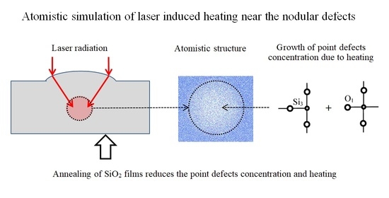
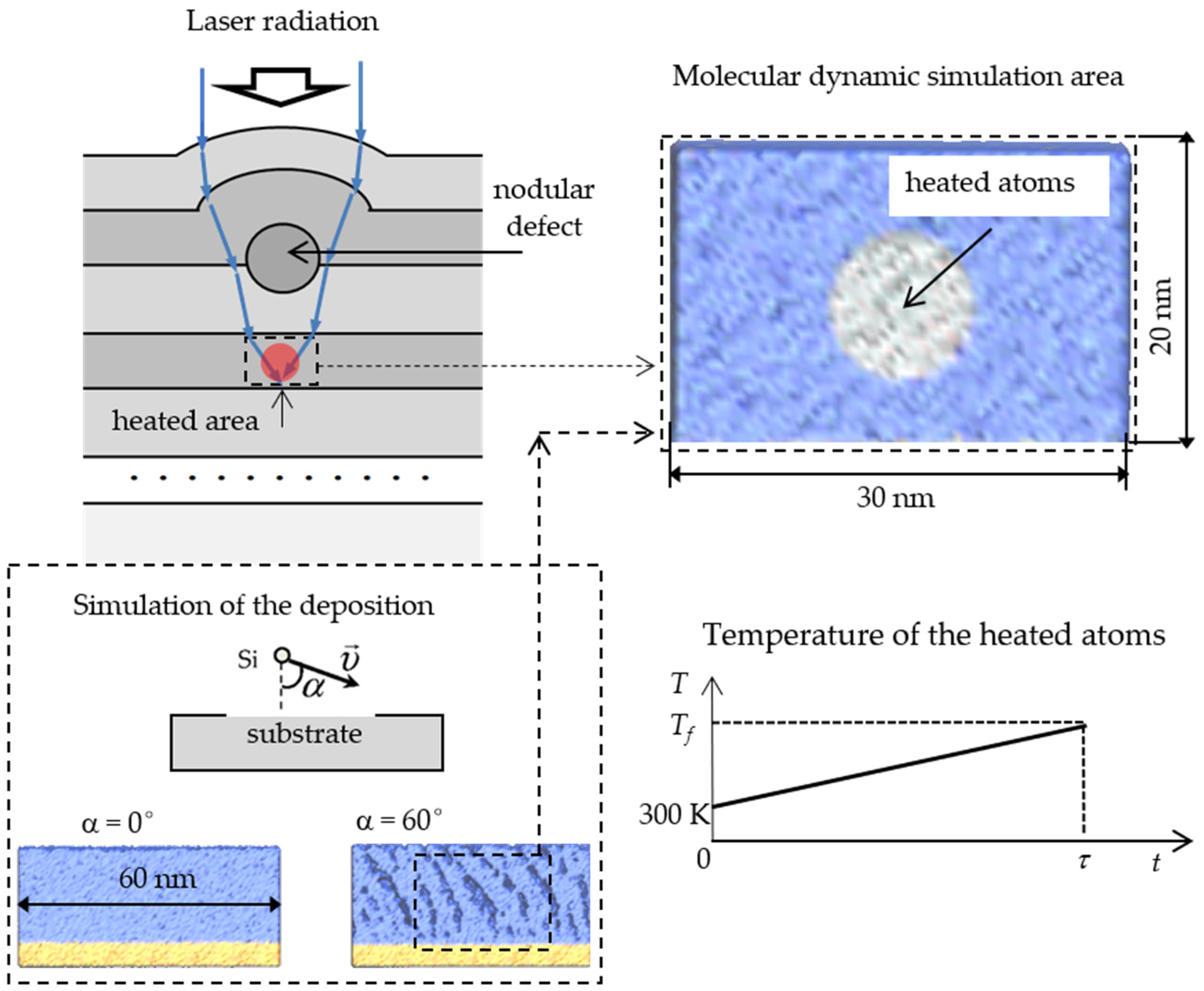
Molecular Dynamics Simulation of Laser Induced Heating of Silicon Dioxide Thin Films

by
Fedor Vasilievich Grigoriev
1,2,*,
Vladimir Borisovich Sulimov
1,2 and
Alexander Vladimirovich Tikhonravov
1,2
1
Research Computing Center, M.V. Lomonosov Moscow State University, Leninskie Gory, 119234 Moscow, Russia
2
Moscow Center for Fundamental and Applied Mathematics, M.V. Lomonosov Moscow State University, Leninskie Gory, 119234 Moscow, Russia
*
Author to whom correspondence should be addressed.
Nanomaterials 2021, 11(11), 2986; https://doi.org/10.3390/nano11112986
Submission received: 6 October 2021 / Revised: 2 November 2021 / Accepted: 3 November 2021 / Published: 6 November 2021
(This article belongs to the Special Issue Nanomaterials Investigation by Molecular Dynamics Simulation)

Abstract

:
The full-atomistic classical molecular dynamics simulation of the laser heating of silicon dioxide thin films is performed. Both dense isotropic films and porous anisotropic films are investigated. It is assumed that heating occurs due to nodal structural defects, which are currently considered one of the possible causes of laser induced damage. It is revealed that heating to a temperature of 1000 K insignificantly affects the structure of the films and the concentration of point defects responsible for the radiation absorption. An increase in the heating temperature to 2000 K leads to the growth of the concentration of these defects. For “as deposited” films, this growth is greater in the case of a porous film deposited at a high deposition angle. Annealing of film reduces the difference in the concentration of laser induced defects in dense and porous films. The possible influence of optical active defects arising due to heating on the laser induced damage threshold is discussed.

Graphical Abstract

1. Introduction

One of the key problems limiting the development of high energy laser systems is laser induced damage (LID) in thin transparent films of optical coatings [1,2,3]. LID is due to the loss of films transparency with an increase in laser impulse power, which leads to an explosive increase in the coating temperature and the subsequent destruction of its structure. To date, theoretical LID models can be divided into two classes: intrinsic and extrinsic [1,4]. Intrinsic models are applied to femtosecond laser pulses with extremely high power. These models take into account the properties of the film materials, such as band-gap values, refractive indices, and so on. The extrinsic models consider defects of structure as the cause of a sharp increase in laser radiation absorption with increasing laser power. These models describe LID from nanoseconds and longer pulses. The difference in the models is based on the experimental observed peculiarities of LID from short and long pulses [5,6].
Initially, the models describing LID were based on continual approaches including heat equations, kinetic equation, Boltzman equation, and so on [1,7,8,9]. In recent decades, due to significant progress in high-performance computing, it has become possible to apply the methods of atomistic simulation for studying the laser radiation interaction with condensed matter [10,11,12]. In the case of femtosecond laser pulses, for this simulation, the quantum methods are required to take into account the probabilities of many-photon absorption, electron tunneling in a strong electric field, and other quantum processes affecting LID [4]. The classic methods of atomistic simulation, such as molecular dynamics (MD), can be applied to study the effect of long pulses on the film structure. In this case, the interaction of laser radiation with electronic subsystem is taken into account through the simulation parameters.
In this work, the MD simulation of laser heating of silicon dioxide thin films is performed. It is assumed that heating occurs due to the amplification of laser radiation by the nodular defects appearing during the deposition process [13,14,15]. These structural defects are currently considered one of the possible causes of laser induced damage [16,17,18]. In [16], the effect of various types of nodules in the Ta2O5/SiO2 coatings on the local absorption of the laser radiation was studied. It was found that this absorption significantly depends on the boundaries of the nodules. In [17], the amplification of the electric field near nodular defects for multilayer mirrors was studied theoretically. This amplification can lead to an increase in the absorption of laser radiation, which affects the value of the LID threshold. In a review paper [18], nodular defects are considered to be the cause of laser induced damage to various types of coatings.
In this paper, we show that MD simulation can offer a description of laser-induced effects near nodular defects at the microscopic level. Both dense films and anisotropic films with high porosity are studied. The temperature and density distributions in the heated area are obtained for different pulse durations. The dependence of the concentration of point defects acting on the radiation absorption on the temperature of the heated area and the pulse duration is investigated. The differences in the effect of laser heating on the structure of as-deposited and annealed films are studied. The results obtained are discussed in terms of the possible causes of extrinsic LID.

2. Simulation Method

The nodular defects in transparent media can focus laser radiation [19], which leads to heating of some portion of the film (see Figure 1). We assume that the temperature of the heated area increases during the entire duration of the pulse. Indeed, the characteristic time τh of thermal energy transfer from the heated area to the substrate can be estimated from the heat equation as τh ~ cρL2/χ, where the values of the specific heat capacity, mass density, and heat conductivity of silicon dioxide are equal to c = 103 J/(kg·K), ρ = 2.2 × 10³ kg/m3, and χ = 2.0 W/(m·K) [20]. Since the characteristic value of film thickness L is about 10−6 m, we obtain τh ~ 10−6 s. This value is much longer than the laser pulse duration; therefore, the stationary regime is not achieved during heating.
Heating of the film is modeled as atomistic clusters having dimensions of 30 × 20 × 20 nm with a total number of atoms of about 6 × 10⁵. The heated area inside the cluster is represented by a sphere with a radius of 5 nm centered in the middle of the cluster. The temperature of atoms inside the sphere is increased linearly from the room temperature 300 K to the final temperature Tf during the pulse duration τ (Figure 1). The initial temperature of atoms outside the sphere is also 300 K, but after the start of heating is not controlled by the thermostat and depends on the heat flux from the heated area. The energy of interatomic interactions is calculated in the frame of the DESIL force field [21]:
U = qiqj/rij + Aij/rij12Bij/rij6
where qi(j) is the charge of the i(j)-th atom, qO = −0.5qSi = −0.65e, Aij and Bij are parameters of the Lennard-Jones potential for the van der Waals interaction, rij is the interatomic distance, ASiO = 4.6·× 10−8 kJ·(nm)12/mol, ASiSi = AOO = 1.5·× 10−6 kJ·(nm)12/mol, BSiO = 4.2·× 10−3 kJ·(nm)6/mol, and BSiSi = BOO = 5·× 10−5 kJ·(nm)6/mol. The step of the molecular dynamic simulation is taken equal to 0.5 fs. Periodic boundary conditions are applied in all directions. To ensure the relaxation of the system volume under the heating conditions, the NPT (constant number of particles, pressure, and temperature) ensemble with Berendsen barostat [22] is used. The value of pressure applied to the boundary of the simulation box is 1 atm.
The atomistic clusters for simulating heating are prepared from the clusters of the silicon dioxide films obtained in our previous work using step-by-step MD procedure [23,24]. In [25], these clusters were used to study thermal stresses arising in thin films due to their heating as a whole. In this work, we study the effects associated with heating in nanoscale regions of atomistic clusters caused by nanoscale nodular defects focusing laser radiation. The simulation of heating is performed with clusters obtained at an energy of incoming Si atoms of 10 eV, which corresponds to the high-energy deposition. Two clusters, deposited at angles α = 0 and 60° are chosen. This is due to the fact that the film structure essentially depends on the deposition angle. Normal deposition at α = 0 produces dense and homogenous structures, while deposition at α = 60° leads to the formation of anisotropic and highly porous films [26].
All simulations are carried out using the GROMACS program [27], installed on the supercomputer “Lomonosov-2” of the HPC computing resources at Lomonosov Moscow State University [28].

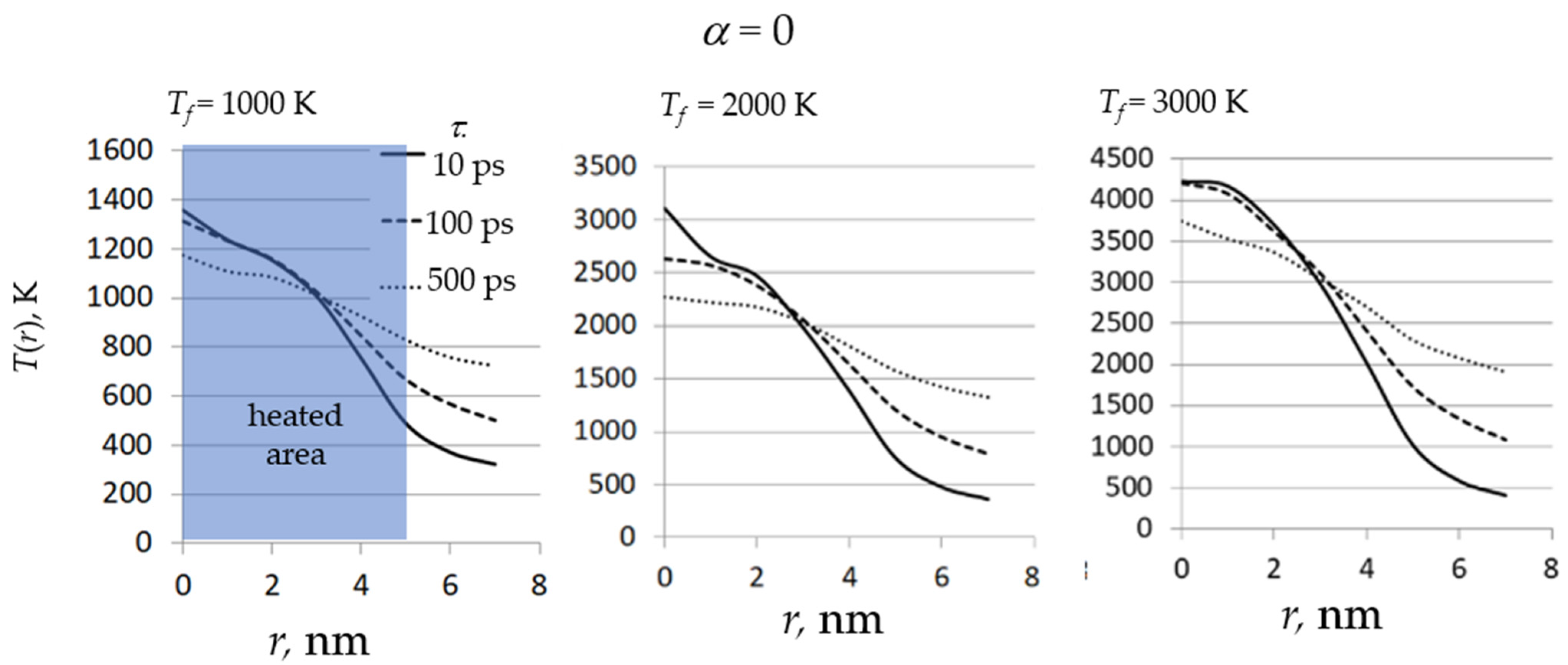
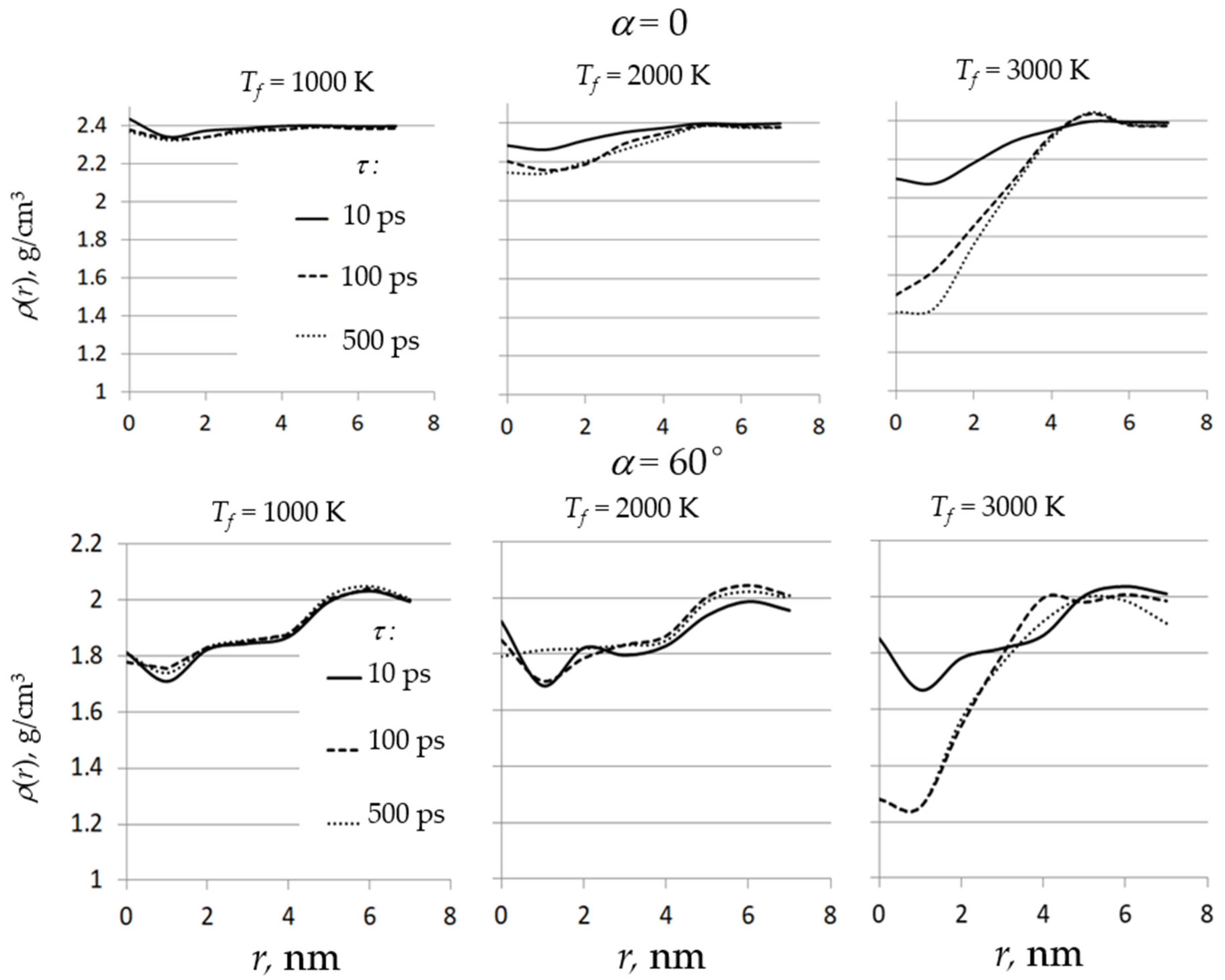
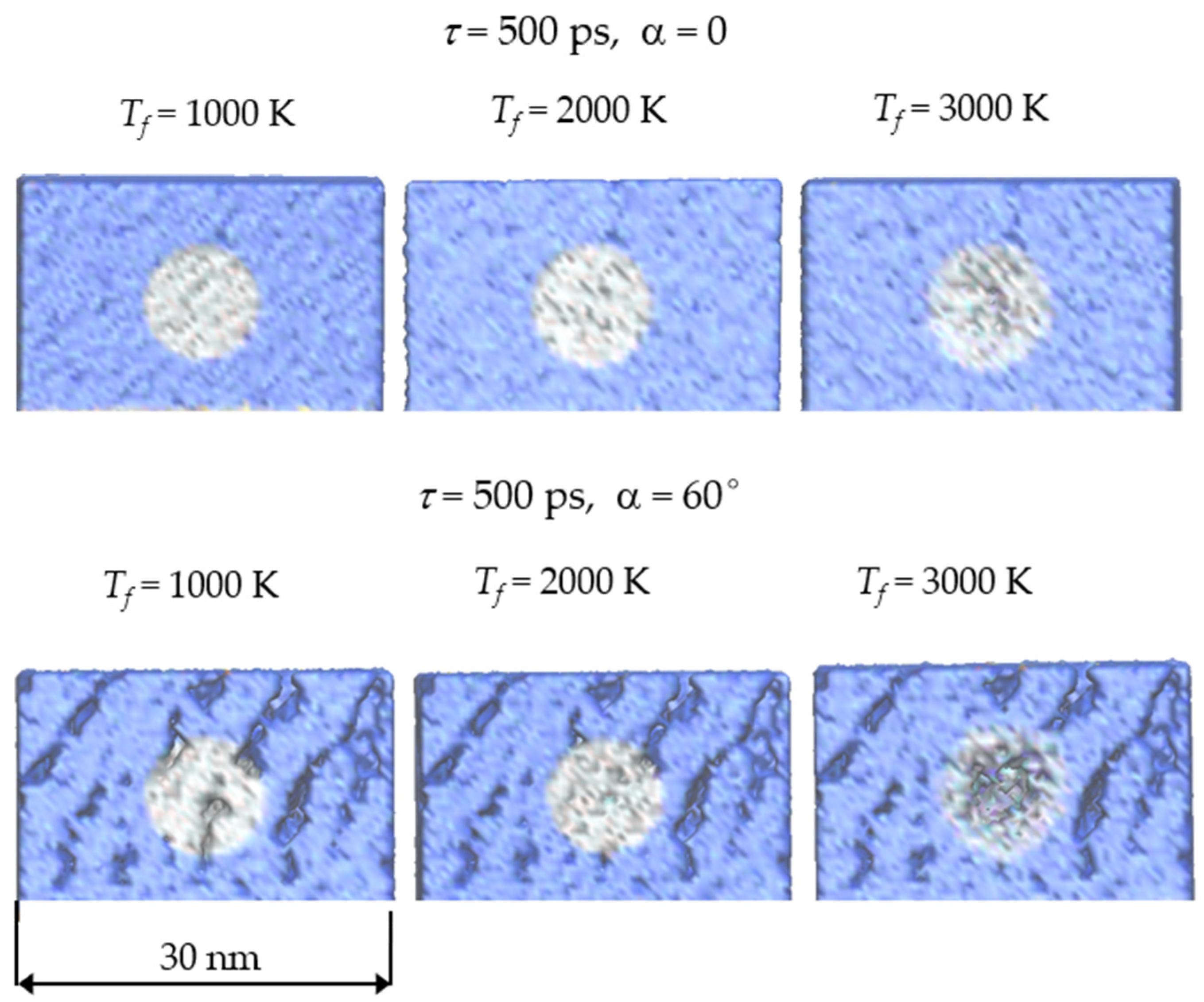
3. Results and Discussion

The simulation results are shown in Figure 2, Figure 3 and Figure 4 and Table 1. In this work, the temperature of the heated area at the end of heating Tf is taken equal to 1000 K, 2000 K, and 3000 K. The minimum value of Tf is close to the temperatures that are used in the thin film annealing after deposition [29], and Tf = 2000 K and 3000 K are about the melting and boiling points of quartz, respectively [30].
The heating time τ is taken to be 10 ps, 100 ps, and 500 ps. A 10 ps value corresponds to short laser pulses with durations from the hundreds of femtoseconds to several picoseconds. It should be taken into account that the laser irradiation interacts with the electron sub-system of matter. The characteristic time of transfer of absorbed energy from the electron sub-system to the nuclei is about several picoseconds [4]. Thus, even for femtosecond laser pulses, the heating time is several picoseconds. In the cases of τ = 100 ps and 500 ps, the heating time can be regarded as the laser pulse duration. Laser pulses with this duration are considered to be long, since their times are much longer than the time of energy transfer from the electron sub-system to the nuclei [4].
The temperature distributions over clusters are shown in Figure 2. To calculate the T(r) values, the average kinetic energy of all atoms between the spheres with radii r and r + ∆r, where ∆r = 1 nm is calculated and inverted into temperature.
As can be seen from the plots in Figure 2, in all cases the temperature decreases monotonically with increasing distance to the center of the heated area. The difference in the temperature of atoms inside and outside of the heated area decreases with an increase in the laser pulse duration. Even at τ = 500 ps, the temperature distributions are far from uniform. In the case of the Tf = 3000 K, the temperature at r < 3 nm exceeds the quartz boiling point, which leads to partial evaporation of the film material, which is confirmed by visualization of the structures (see Figure 4). Since there are no noticeable differences in the temperature distributions in the case of α = 60° compared to α = 0°, the data are presented only for the normally deposited film.
The density distributions ρ (r) are shown in Figure 3. The ρ (r) is equal to the density inside the area between spheres with radii r and r + ∆r, where ∆r = 1 nm. The density profiles at heating temperature Tf = 1000 K change insignificantly with increasing heating time τ and correspond to the profiles of the unheated films. The difference in the density of films deposited at α = 0 and α = 60° (see the upper and lower plots in the left column in Figure 3) is caused by the difference in the deposition angles and is not related to heating.
An increase in the heating temperature to Tf = 2000 K leads to changes in the density profiles of the most heated region near r = 0. In a dense film (α = 0), the density decreases essentially with increasing heating time from τ = 10 ps to τ = 100 ps. A further increase of τ to 500 ps has no significant effect on the density profile. In the case of a porous SiO2 film (α = 60°), heating to Tf = 2000 K for 500 ps leads to smoothing of the density profiles at r < 2 nm. Visual analysis reveals that this heating leads to the disappearance of the large pore in the center of the heated area (see the bottom row in Figure 4).
An increase in the heating temperature to Tf = 3000 K leads to the sharp decrease in the density near the center of the heated area for both films. This is due to the start of the boiling process, since the temperature near the center of the heated area exceeds the quartz boiling point.
Heating of the films can lead to an increase in the concentration of point defects, such as oxygen-deficient silicon Si3 and nonbridging oxygen center O1. The experimentally observed absorption and luminescence at photon energies below the band-gap of silica is attributed to these defects [31,32]. Thus, an increase in the concentration of these defects leads to an increase in absorption, which increases the heating of the film. Ultimately, this can lead to a thermal explosion destroying the structure.
The values of the point defects concentration are presented in Table 1. The concentration of O1 and Si3 centers in the “as deposited” films at room temperature at α = 60° is almost twice as high as at α = 0. This difference is explained by the high porosity of the film deposited at α = 60°, which leads to an increase in the concentration of the defects. As can be seen from the data in Table 1, this noticeable difference persists under heating.
Heating to Tf = 1000 K insignificantly affects the concentration of O1 and Si3 centers. An increase in the final value of the heating temperature to Tf = 2000 K leads to a noticeable increase in the concentration of defects, primarily of Si3 centers. An increase in the heating time from τ = 100 ps to τ = 500 ps at Tf = 2000 K also leads to an increase in the defects concentration. For a normally deposited film, heating to Tf = 3000 K at τ = 500 ps is accompanied by an increase in c(O1) and c(Si3) by approximately four and twenty times, respectively, compared with the values in the film at room temperature. In the case of α = 60°, the relative increase in the of c(O1) and c(Si3) values caused by heating at Tf = 3000 K and τ = 500 ps is slightly higher than in the case of a normally deposited film.
Annealing of the films significantly affects the c(O1) and c(Si3) values (see the lower part of Table 1). In this work, annealing is simulated as described in [33] at an annealing temperature of 1300 K during 1 ns. As expected, annealing reduces the c(O1) and c(Si3) values. This decrease is more noticeable for a porous film deposited at α = 60°. On the whole, the tendency towards an increase in the defects concentration with an increase in the heating temperature and heating time is retained for the annealed films. At the same time, preliminary annealing of the films reduces the differences in c(O1) and c(Si3) values for the films deposited at α = 60° and α = 0. For instance, c(O1) = 2.46 (α = 0°) and c(O1) = 2.55 (α = 60°) at Tf = 2000 K and τ = 500 ps.
Let us discuss the obtained results from the point of view of the LID problem. Heating to an average temperature Tf = 1000 K insignificantly affects the structure of the films, including the concentration of point defects. For this reason, this heating does not initiate LID. This is true both for a normally deposited dense film and for a highly porous film deposited at α = 60°.
Heating to Tf = 2000 K is accompanied by a noticeable increase in the concentration of optical active defects. This growth is observed at all values of the laser pulse duration. This leads to an increase in the radiation absorption, which is accompanied by an increase in the film temperature, which ultimately can lead to a thermal explosion. Thus, this heating can initiate LID. In the case of “as deposited” films, the concentration of the laser induced defects in porous film deposited at α = 60° increases more than in a normally deposited film. Thus, for porous films, the threshold value of LID can be lower.
Annealing the films before heating leads to a decrease in the difference of the defects concentration in films deposited at α = 0 and α = 60°, so the difference in the LID threshold for these films can also decrease. In addition, the inhomogeneity of the structure of the porous film can partially prevent the focusing of laser beam by nodular defects. For this reason, the heating temperature of a porous film can be lower than that for a dense film at the same values of the radiation power. Thus, the porous film can be even more LID-resistant than the dense film. An increase in the laser induced damage threshold with an increase in the deposition angle and film porosity was observed experimentally for SiO2 films [34,35]. To summarize, an increase in the concentration of point defects due to heating near the nodular defects can be noted. This increase depends on film structure. It is shown that post deposition annealing reduces the concentration of point defects, and thus can reduce the negative effect of nodular defects on the LID threshold.

4. Conclusions

In this work, the atomistic simulation of the laser induced heating of the silicon dioxide thin films is performed. Heating is caused by focusing the laser beam by the nodular defects in the film structure.
It is found that heating to 1000 K for 500 ps insignificantly affects the structure of the films and concentration of the optical active point defects. An increase in the heating temperature to 2000 K leads to an increase in the concentration of point defects, especially oxygen-deficient silicon Si3. For “as deposited” films, this increase is greater in the case of a porous film deposited at a large deposition angle. Annealing the films reduces the difference in the concentration of laser induced defects for dense and porous films.

Author Contributions

Author Contributions: Conceptualization, A.V.T., F.V.G., V.B.S.; methodology, F.V.G.; software, F.V.G. and V.B.S.; validation, F.V.G.; formal analysis, F.V.G.; investigation, F.V.G.; resources, A.V.T. and V.B.S.; data curation, A.V.T. and V.B.S.; writing—original draft preparation, F.V.G.; writing—review and editing, A.V.T. and V.B.S.; visualization, F.V.G.; supervision, A.V.T. and V.B.S.; project administration, V.B.S.; funding acquisition, A.V.T. and V.B.S. All authors have read and agreed to the published version of the manuscript.

Funding

The work was supported by the Russian Science Foundation (grant no. 19-11-00053). The part of the work related to organization and optimization of the supercomputer calculations was supported by the Russian Ministry of Science and Higher Education, agreement no. 075-15-2019-1621.

Institutional Review Board Statement

Not applicable.

Informed Consent Statement

Not applicable.

Data Availability Statement

Not applicable.

Acknowledgments

Not applicable.

Conflicts of Interest

The authors declare no conflict of interest.

References

  1. Manenkov, A.A. Fundamental mechanisms of laser-induced damage in optical materials: Today’s state of understanding and problems. Opt. Eng. 2014, 53, 010901. [Google Scholar] [CrossRef]
  2. Gallais, L.; Douti, D.-B.; Commandré, M.; Batavičiūtė, G.; Pupka, E.; Ščiuka, M.; Smalakys, L.; Sirutkaitis, V.; Melninkaitis, A. Wavelength dependence of femtosecond laser-induced damage threshold of optical materials. J. Appl. Phys. 2015, 117, 223103. [Google Scholar] [CrossRef] [Green Version]
  3. Velpula, P.K.; Kramer, D.; Rus, B. Femtosecond Laser-Induced Damage Characterization of Multilayer Dielectric Coatings. Coatings 2020, 10, 603. [Google Scholar] [CrossRef]
  4. Chorel, M. Study of High Damage Threshold Optical Coatings Used in Environment with Very Low Hygrometry for Fusion Class Laser System. Optics/Photonic. Ph.D. Thesis, Université de Bordeaux, Bordeaux, France, 2019. (In English). [Google Scholar]
  5. Kozlowski, M.R.; Chow, R. Role of defects in laser damage of multilayer coatings. In Proceedings of the Volume 2114, Laser-Induced Damage in Optical Materials: 1993, Boulder, CO, USA, 28 July 1994. [Google Scholar] [CrossRef] [Green Version]
  6. Papernov, S. Laser-Induced Damage in Optical Materials, Chapter Defect-Induced Damage; CRC Press: Boca Raton, FL, USA, 2015; pp. 25–75. [Google Scholar]
  7. Yang, H.; Cheng, J.; Liu, Z.; Liu, Q.; Zhao, L.; Wang, J.; Chen, M. Dynamic behavior modeling of laser-induced damage initiated by surface defects on KDP crystals under nanosecond laser irradiation. Sci. Rep. 2020, 10, 500. [Google Scholar] [CrossRef] [PubMed] [Green Version]
  8. Chen, M.; Ding, W.; Cheng, J.; Yang, H.; Liu, Q. Recent Advances in Laser-Induced Surface Damage of KH2PO4 Crystal. Appl. Sci. 2020, 10, 6642. [Google Scholar] [CrossRef]
  9. Rouquette, P.; Amra, C.; Zerrad, M.; Grèzes-Besset, C. Photo-induced thermal radiation within multilayers optics. In Proceedings of the SPIE 11872, Advances in Optical Thin Films VII, Online, 12 September 2021. [Google Scholar] [CrossRef]
  10. Klein, D.; Eisfeld, E.; Roth, J. Molecular dynamics simulations of the laser ablation of silicon with the thermal spike model. J. Phys. D Appl. Phys. 2021, 54, 015103. [Google Scholar] [CrossRef]
  11. Wang, X.; Xu, X. Molecular Dynamics Simulation of Heat Transfer and Phase Change During Laser Material Interaction. J. Heat Transf. 2002, 124, 265–274. [Google Scholar] [CrossRef]
  12. Huang, C.; Cheng, Y.; Yin, H.; Wei, F. Molecular dynamics simulation of laser-induced interconnections of silver nanowires. Ferroelectrics 2020, 564, 91–101. [Google Scholar] [CrossRef]
  13. Dubost, L.; Rhallabi, A.; Perrin, J.; Schmitt, J. Growth of nodular defects during film deposition. J. Appl. Phys. 1995, 78, 3784. [Google Scholar] [CrossRef]
  14. Panjan, P.; Drnovšek, A.; Gselman, P.; Cekada, M.; Panjan, M. Review of Growth Defects in Thin Films Prepared by PVD Techniques. Coatings 2020, 10, 447. [Google Scholar] [CrossRef]
  15. Liu, X.; Li, D.; Zhao, Y.; Li, X. Further investigation of the characteristics of nodular defects. Appl. Opt. 2010, 49, 1774–1779. [Google Scholar] [CrossRef] [PubMed] [Green Version]
  16. Ma, H.; Cheng, X.; Zhang, J.; Jiao, H.; Ma, B.; Tang, Y.; Wu, Z.; Wang, Z. Effect of boundary continuity on nanosecond laser damage of nodular defects in high-reflection coatings. Opt. Lett. 2017, 42, 478–481. [Google Scholar] [CrossRef] [PubMed]
  17. Stolz, C.J.; Feigenbaum, E. Impact of high refractive coating material on the nodular-induced electric field enhancement for near infrared multilayer mirrors. Appl. Opt. 2020, 59, A20–A25. [Google Scholar] [CrossRef]
  18. Stolz, C.J.; Negres, R.A. Ten-year summary of the Boulder Damage Symposium annual thin film laser damage competition. Opt. Eng. 2018, 57, 121910. [Google Scholar] [CrossRef]
  19. Milward, J.R.; Lewis, K.L.; Pitt, A.M.; Kirton, J.; Overend, R.B.; Gibson, D.R.; Leonard, J.; Hendry, A. Laser damage issues for mid-IR optical parametric oscillator mirrors. In Proceedings of the SPIE 2114, Laser-Induced Damage in Optical Materials: 1993, Boulder, CO, USA, 28 July 1994. [Google Scholar] [CrossRef]
  20. Leko, V.K.; Mazurin, O.V. Properties of Quartz Glass; Nauka: Leningrad, Russian, 1985. (In Russian) [Google Scholar]
  21. Grigoriev, F.V.; Sulimov, A.V.; Kochikov, I.V.; Kondakova, O.A.; Sulimov, V.B.; Tikhonravov, A.V. Supercomputer modeling of the ion beam sputtering process: Full-atomistic level. In Proceedings of the SPIE—The International Society for Optical Engineering, Jena, Germany, 23 September 2015; Volume 9627. [Google Scholar] [CrossRef]
  22. Berendsen, H.J.C.; Postma, J.P.M.; van Gunsteren, W.F.; DiNola, A.; Haak, J.R. Molecular-Dynamics with Coupling to an External Bath. J. Chem. Phys. 1984, 81, 3684–3690. [Google Scholar] [CrossRef] [Green Version]
  23. Grigoriev, F.V.; Sulimov, V.B.; Tikhonravov, A.V. Atomistic simulation of the glancing angle deposition of SiO2 thin films. J. Non-Cryst. Solids 2019, 512, 98–102. [Google Scholar] [CrossRef]
  24. Grigoriev, F.V.; Sulimov, V.B.; Tikhonravov, A.V. Structure of Highly Porous Silicon Dioxide Thin Film: Results of Atomistic Simulation. Coatings 2019, 9, 568–576. [Google Scholar] [CrossRef] [Green Version]
  25. Grigoriev, F.V.; Sulimov, V.B.; Tikhonravov, A.V. Laser-Induced Thermal Stresses in Dense and Porous Silicon Dioxide Films. Coatings 2020, 11, 394. [Google Scholar] [CrossRef]
  26. Robbie, K.; Brett, M.J.; Lakhtakia, A. Chiral sculptured thin films. Nature 1996, 384, 616. [Google Scholar] [CrossRef]
  27. Abraham, M.J.; Murtola, T.; Schulz, R.; Páll, S.; Smith, J.C.; Hess, B.; Lindahl, E. GROMACS: High performance molecular simulations through multi-level parallelism from laptops to supercomputers. SoftwareX 2015, 1–2, 19–25. [Google Scholar] [CrossRef] [Green Version]
  28. Voevodin, V.L.; Antonov, A.; Nikitenko, D.; Shvets, P.; Sobolev, S.; Sidorov, I.; Stefanov, K.; Voevodin, V.; Zhumatiy, S. Supercomputer Lomonosov-2: Large Scale, Deep Monitoring and Fine Analytics for the User Community. Supercomput. Front. Innov. 2019, 6, 4–11. [Google Scholar] [CrossRef] [Green Version]
  29. Taniguchi, K.; Tanaka, M.; Hamaguchi, C.; Imai, K. Density relaxation of silicon dioxide on (100) silicon during thermal annealing. J. Appl. Phys. 1990, 67, 2195–2198. [Google Scholar] [CrossRef]
  30. Perry, D.L. Handbook of Inorganic Compounds; CRC Press: Boca Raton, FL, USA, 2016; 581p. [Google Scholar]
  31. Bakos, T.; Rashkeev, S.N.; Pantelides, S.T. Optically active defects in SiO2: The nonbridging oxygen center and the interstitial OH molecule. Phys. Rev. B 2004, 70, 075203. [Google Scholar] [CrossRef]
  32. Skuja, L. Optically active oxygen-deficiency-related centers in amorphous silicon dioxide. J. Non-Cryst. Solids 1998, 239, 16–48. [Google Scholar] [CrossRef]
  33. Grigoriev, F.V.; Sulimov, A.V.; Katkova, E.V.; Kochikov, I.V.; Kondakova, O.A.; Sulimov, V.B.; Tikhonravov, A.V. Annealing of deposited SiO2 thin films: Full-atomistic simulation results. Opt. Mater. Express 2016, 6, 3960–3966. [Google Scholar] [CrossRef]
  34. Melninkaitis, A.; Grinevičiūtė, L.; Abromavičius, G.; Mažulė, L.; Smalakys, L.; Pupka, E.; Ščiuka, M.; Buzelis, R.; Kičas, S.; Tolenis, T. Next-generation allsilica coatings for UV applications. In Proceedings of the SPIE 10447, Laser-Induced Damage in Optical Materials, Boulder, CO, USA, 13 November 2017. [Google Scholar] [CrossRef]
  35. Ramalis, L.; Norkutė, U.; Buzelis, R.; Selskis, A.; Tolenis, T. Sculptured thin film based all-silica mirrors for high power lasers. In Proceedings of the SPIE 11872, Advances in Optical Thin Films VII, Online, 12 September 2021. [Google Scholar] [CrossRef]
Figure 1. Scheme for modeling laser induced thin film heating.
Nanomaterials 11 02986 g001
Figure 2. Dependence of the temperature T on the distance from the center of the heated area r, where τ is the heating time, Tf is the final temperature, and α is the deposition angle.
Nanomaterials 11 02986 g002
Figure 3. Dependence of the density ρ on the distance from the center of the heated area r, where τ is the heating time, Tf is the final temperature, and α is the deposition angle.
Nanomaterials 11 02986 g003
Figure 4. The final structures of the heated clusters for different values of the temperature Tf and deposition angle α, where τ is the heating time.
Nanomaterials 11 02986 g004
Table 1. Concentration of defects c(O1) and c(Si3) (%, lower index is equal to the coordination number) in films at different deposition and heating conditions, where Tf is the final heating temperature, τ is the heating time, α increase s the deposition angle, and T0 is the film temperature before heating.
“As Deposited” Films
ατ, psDefectT0 = 300 K
(before Heating)
Tf, K
100020003000
010c(O1)1.131.171.432.26
c(Si3)0.350.320.872.50
100c(O1) 1.161.442.70
c(Si3)0.300.913.54
500c(O1)1.121.614.69
c(Si3)0.361.627.52
6010c(O1)2.172.203.256.35
c(Si3)0.750.863.038.20
100c(O1) 2.193.538.40
c(Si3)0.903.8212.05
500c(O1)2.123.3211.08
c(Si3)0.924.3518.11
Annealed Films
ατ, psDefectT0 = 300 K
(before heating)
Tf, K
100020003000
010c(O1)1.041.031.884.90
c(Si3)0.470.502.077.17
100c(O1) 1.052.297.40
c(Si3)0.502.8711.38
500c(O1)1.042.4610.48
c(Si3)0.513.4417.50
6010c(O1)1.421.452.395.24
c(Si3)0.670.922.837.57
100c(O1) 1.362.586.99
c(Si3)0.893.4610.63
500c(O1)1.362.559.95
c(Si3)0.893.7216.76
Publisher’s Note: MDPI stays neutral with regard to jurisdictional claims in published maps and institutional affiliations.

