
Strain and Spin-Orbit Coupling Engineering in Twisted WS2/Graphene Heterobilayer


 , ,
, ,
Abstract
:1. Introduction
2. Materials and Methods
3. Results and Discussion
- (i)
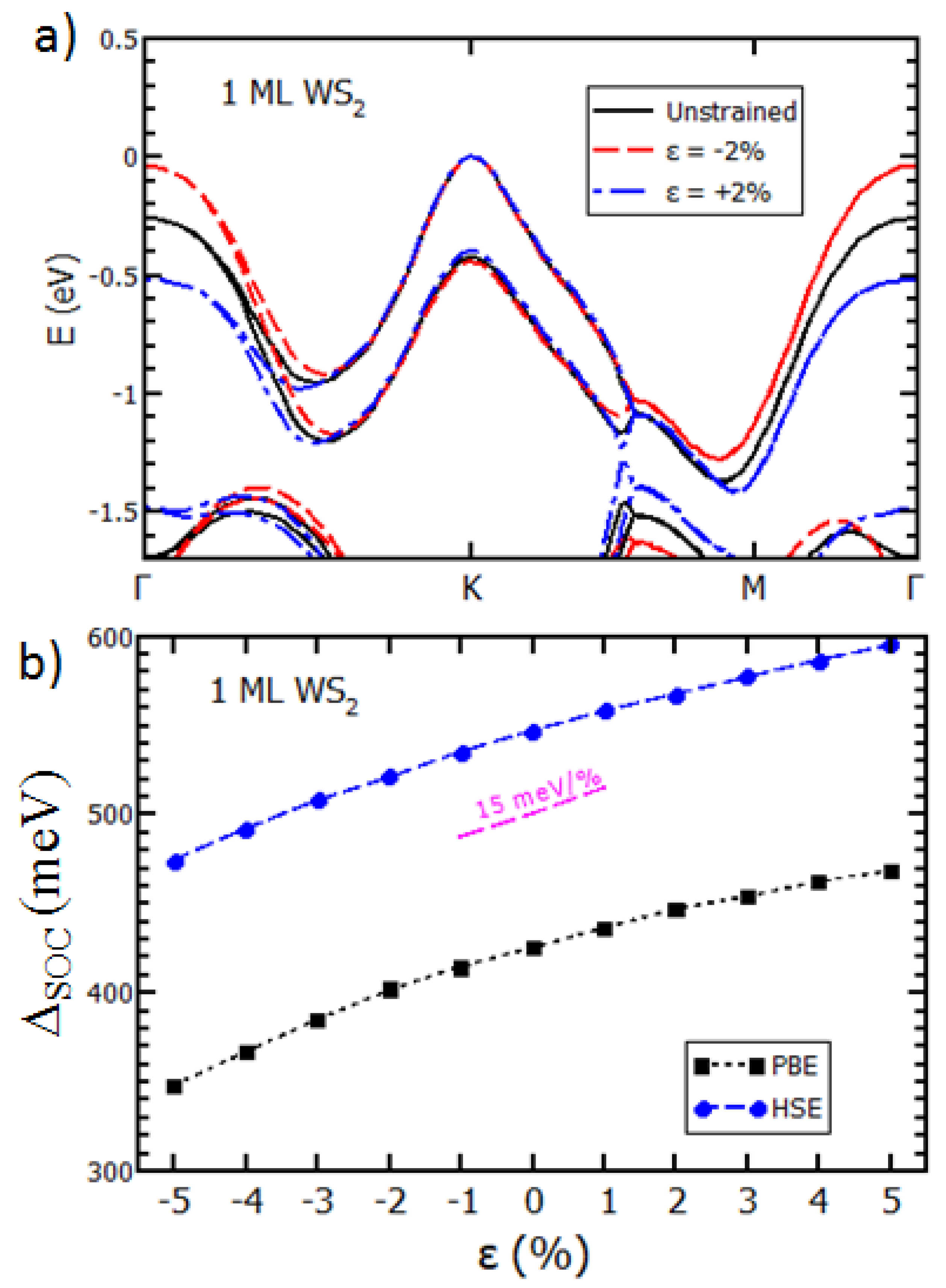
- First, we can consider the charge transfer probabilities occurring at specific twist angles as the main contribution to the ΔSOC variations. In the present case, the heterostructure is formed by n-type graphene and n-type WS2, which creates a Schottky barrier. The Schottky barrier height (SBH) thus corresponds to the energy difference between the CBM of the WS2 band, and the position of the Fermi level in the graphene Dirac cone [4]. Since the graphene layer is n-doped, a charge transfer could occur from the K valley of the graphene to the CBM of the WS2. Following [15,16], the interlayer interaction between WS2 and Gr is proportional to the transfer integral between the two lattices, which decreases exponentially with the interlayer spacing in real space, but also requires momentum matching in the reciprocal space. As illustrated in Supplementary Information (Figure S3), the positions of three specific k-vectors in the BZ of WS2 vary with the twist angle (red circles) and can approach the CBM of WS2 (green symbols). It turns out that the interlayer coupling and, hence, the spin-splitting of WS2, is maximal when the wavevectors, , , and , approach the CBM of the WS2 located in the Q point (middle point between Γ and K) for θ~20°. While this effect may occur in our structures, the expected order of magnitude (a few meV) and angular positions do not match our experiments. Therefore, charge transfer is not the main contributor to the observed ΔSOC variations;
- (ii)
- Mechanical strain is an expected feature of vdW heterostructures, which assemble materials of different lattice parameters. Although the vdW interaction is weaker than covalent bounds, it can still create Moiré superlattices that can affect the material strain and its electronic properties. The superstructure is governed by the lattice mismatch and by the rotational and translational misalignments of the two lattices. Here, the observed angular misalignment, θ WS2/Gr, combined with the theoretical lattice mismatch, (aGr~2.46 Å, aWS2~3.16 Å), can create a long-range strain modulation, which can be grossly approximated to a uniform tensile or compressive in-plane strain [37].
4. Conclusions
Supplementary Materials
Author Contributions
Funding
Institutional Review Board Statement
Data Availability Statement
Conflicts of Interest
References
- Novoselov, K.S.; Geim, A.K.; Morozov, S.V.; Jiang, D.; Katsnelson, M.I.; Grigorieva, I.V.; Dubonos, S.V.; Firsov, A.A. Two-Dimensional Gas of Massless Dirac Fermions in Graphene. Nature 2005, 438, 197–200. [Google Scholar] [CrossRef] [PubMed]
- Zhang, K.; Zhang, T.; Cheng, G.; Li, T.; Wang, S.; Wei, W.; Zhou, X.; Yu, W.; Sun, Y.; Wang, P.; et al. Interlayer Transition and Infrared Photodetection in Atomically Thin Type-II MoTe2/MoS2van Der Waals Heterostructures. ACS Nano. 2016, 10, 3852–3858. [Google Scholar] [CrossRef]
- Cao, Y.; Fatemi, V.; Fang, S.; Watanabe, K.; Taniguchi, T.; Kaxiras, E.; Jarillo-Herrero, P. Unconventional Superconductivity in Magic-Angle Graphene Superlattices. Nature 2018, 556, 43–50. [Google Scholar] [CrossRef]
- Pierucci, D.; Henck, H.; Avila, J.; Balan, A.; Naylor, C.H.; Patriarche, G.; Dappe, Y.J.; Silly, M.G.; Sirotti, F.; Johnson, A.T.C.; et al. Band Alignment and Minigaps in Monolayer MoS2-Graphene van Der Waals Heterostructures. Nano. Lett. 2016, 16, 4054–4061. [Google Scholar] [CrossRef]
- Wang, L.; Shih, E.M.; Ghiotto, A.; Xian, L.; Rhodes, D.A.; Tan, C.; Claassen, M.; Kennes, D.M.; Bai, Y.; Kim, B.; et al. Correlated Electronic Phases in Twisted Bilayer Transition Metal Dichalcogenides. Nat. Mater. 2020, 19, 861–866. [Google Scholar] [CrossRef] [PubMed]
- Hesp, N.C.H.; Torre, I.; Rodan-Legrain, D.; Novelli, P.; Cao, Y.; Carr, S.; Fang, S.; Stepanov, P.; Barcons-Ruiz, D.; Herzig-Sheinfux, F.; et al. Collective excitations in twisted bilayer graphene close to the magic angle. Nat. Phys. 2019. [Google Scholar] [CrossRef]
- Rivera, P.; Schaibley, J.R.; Jones, A.M.; Ross, J.S.; Wu, S.; Aivazian, G.; Klement, P.; Seyler, K.; Clark, G.; Ghimire, N.J.; et al. Observation of Long-Lived Interlayer Excitons in Monolayer MoSe2-WSe2 Heterostructures. Nat. Commun. 2015, 6, 6242. [Google Scholar] [CrossRef] [PubMed] [Green Version]
- Bradford, J.; Shafiei, M.; MacLeod, J.; Motta, N. Synthesis and characterization of WS2/graphene/SiC van der Waals heterostructures via WO3−x thin film sulfurization. Sci. Rep. 2020, 10, 17334. [Google Scholar] [CrossRef]
- Forti, S.; Rossi, A.; Büch, H.; Cavallucci, T.; Bisio, F.; Sala, A.; Menteş, T.O.; Locatelli, A.; Magnozzi, M.; Canepa, M.; et al. Electronic Properties of Single-Layer Tungsten Disulfide on Epitaxial Graphene on Silicon Carbide. Nanoscale 2017, 9, 16412–16419. [Google Scholar] [CrossRef] [PubMed] [Green Version]
- Rossi, A.; Spirito, D.; Bianco, F.; Forti, S.; Fabbri, F.; Büch, H.; Tredicucci, A.; Krahne, R.; Coletti, C. Patterned Tungsten Disulfide/Graphene Heterostructures for Efficient Multifunctional Optoelectronic Devices. Nanoscale 2018, 10, 4332–4338. [Google Scholar] [CrossRef] [Green Version]
- Henck, H.; Pierucci, D.; Chaste, J.; Naylor, C.H.; Avila, J.; Balan, A.; Silly, M.G.; Maria, C.; Sirotti, F.; Johnson, A.T.C.; et al. Electrolytic Phototransistor Based on Graphene-MoS2 van Der Waals p-n Heterojunction with Tunable Photoresponse p-n Heterojunction with Tunable Photoresponse. Appl. Phys. Lett. 2016, 109, 113103. [Google Scholar] [CrossRef] [Green Version]
- Ghiasi, T.S.; Kaverzin, A.A.; Blah, P.J.; Van Wees, B.J. Charge-to-Spin Conversion by the Rashba-Edelstein Effect in Two-Dimensional van Der Waals Heterostructures up to Room Temperature. Nano. Lett. 2019, 19, 5959–5966. [Google Scholar] [CrossRef] [Green Version]
- Avsar, A.; Tan, J.Y.; Taychatanapat, T.; Balakrishnan, J.; Koon, G.K.W.; Yeo, Y.; Lahiri, J.; Carvalho, A.; Rodin, A.S.; O’Farrell, E.C.T.; et al. Spin-Orbit Proximity Effect in Graphene. Nat. Commun. 2014, 5, 4875. [Google Scholar] [CrossRef]
- Wakamura, T.; Reale, F.; Palczynski, P.; Zhao, M.Q.; Johnson, A.T.C.; Guéron, S.; Mattevi, C.; Ouerghi, A.; Bouchiat, H. Spin-Orbit Interaction Induced in Graphene by Transition Metal Dichalcogenides. Phys. Rev. B 2019, 99, 245402. [Google Scholar] [CrossRef] [Green Version]
- David, A.; Rakyta, P.; Kormányos, A.; Burkard, G. Induced Spin-Orbit Coupling in Twisted Graphene-Transition Metal Dichalcogenide Heterobilayers: Twistronics Meets Spintronics. Phys. Rev. B 2019, 100, 85412. [Google Scholar] [CrossRef] [Green Version]
- Li, Y.; Koshino, M. Twist-Angle Dependence of the Proximity Spin-Orbit Coupling in Graphene on Transition-Metal Dichalcogenides. Phys. Rev. B 2019, 99, 075438. [Google Scholar] [CrossRef] [Green Version]
- Henck, H.; Ben Aziza, Z.; Pierucci, D.; Laourine, F.; Reale, F.; Palczynski, P.; Chaste, J.; Silly, M.G.; Bertran, F.; Le Fèvre, P.; et al. Electronic Band Structure of Two-Dimensional WS2/Graphene van Der Waals Heterostructures. Phys. Rev. B 2018, 97, 155421. [Google Scholar] [CrossRef] [Green Version]
- Nguétchuissi Noumbé, U.; Gréboval, C.; Livache, C.; Brulé, T.; Doudin, B.; Ouerghi, A.; Lhuillier, E.; Dayen, J.-F. Ionic Glass–Gated 2D Material–Based Phototransistor: MoSe2 over LaF3 as Case Study. Adv. Funct. Mater. 2019, 29, 1902723. [Google Scholar] [CrossRef]
- Giannozzi, P.; Baroni, S.; Bonini, N.; Calandra, M.; Car, R.; Cavazzoni, C.; Ceresoli, D.; Chiarotti, G.L.; Cococcioni, M.; Dabo, I.; et al. QUANTUM ESPRESSO: A Modular and Open-Source Software Project for Quantum Simulations of Materials. J. Phys. Condens. Matter 2009, 21, 395502. [Google Scholar] [CrossRef] [PubMed]
- Heyd, J.; Scuseria, G.E.; Ernzerhof, M. Hybrid Functionals Based on a Screened Coulomb Potential. J. Chem. Phys. 2003, 118, 8207. [Google Scholar] [CrossRef] [Green Version]
- Zribi, J.; Khalil, L.; Avila, J.; Chaste, J.; Henck, H.; Oehler, F.; Gil, B.; Liu, S.; Edgar, J.H.; Giorgetti, C.; et al. Structural and Electronic Transitions in Few Layers of Isotopically Pure Hexagonal Boron Nitride. Phys. Rev. B 2020, 102, 115141. [Google Scholar] [CrossRef]
- Zribi, J.; Khalil, L.; Zheng, B.; Avila, J.; Pierucci, D.; Brulé, T.; Chaste, J.; Lhuillier, E.; Asensio, M.C.; Pan, A.; et al. Strong Interlayer Hybridization in the Aligned SnS2/WSe2 Hetero-Bilayer Structure. Npj 2d Mater. Appl. 2019, 3, 27. [Google Scholar] [CrossRef] [Green Version]
- Kobayashi, Y.; Sasaki, S.; Mori, S.; Hibino, H.; Liu, Z.; Watanabe, K.; Taniguchi, T.; Suenaga, K.; Maniwa, Y.; Miyata, Y. Growth and Optical Properties of High-Quality Monolayer WS2 on Graphite. ACS Nano. 2015, 9, 4056–4063. [Google Scholar] [CrossRef]
- Gutiérrez, H.R.; Perea-López, N.; Elías, L.A.; Berkdemir, A.; Wang, B.; Terrones, M. Extraordinary Room-Temperature Photoluminescence in Triangular WS2 Monolayers. Nano. Lett. 2013, 13, 3447–3454. [Google Scholar] [CrossRef] [Green Version]
- Molina-Sánchez, A.; Wirtz, L. Phonons in Single-Layer and Few-Layer MoS2 and WS2. Phys. Rev. B 2011, 84, 155413. [Google Scholar] [CrossRef] [Green Version]
- Ernandes, C.; Khalil, L.; Almabrouk, H.; Pierucci, D.; Zheng, B.; Avila, J.; Dudin, P.; Chaste, J.; Oehler, F.; Pala, M.; et al. Indirect to Direct Band Gap Crossover in Two-Dimensional WS2(1−x)Se2x Alloys. Npj 2d Mater. Appl. 2021, 5, 1–7. [Google Scholar] [CrossRef]
- Lorchat, E.; López, L.E.P.; Robert, C.; Lagarde, D.; Froehlicher, G.; Taniguchi, T.; Watanabe, K.; Marie, X.; Berciaud, S. Filtering the Photoluminescence Spectra of Atomically Thin Semiconductors with Graphene. Nat. Nanotechnol. 2020, 15, 283–288. [Google Scholar] [CrossRef] [Green Version]
- Yang, B.; Molina, E.; Kim, J.; Barroso, D.; Lohmann, M.; Liu, Y.; Xu, Y.; Wu, R.; Bartels, L.; Watanabe, K.; et al. Effect of Distance on Photoluminescence Quenching and Proximity-Induced Spin-Orbit Coupling in Graphene/WSe2 Heterostructures. Nano. Lett. 2018, 18, 3580–3585. [Google Scholar] [CrossRef] [PubMed] [Green Version]
- Froehlicher, G.; Lorchat, E.; Berciaud, S. Charge Versus Energy Transfer in Atomically Thin Graphene-Transition Metal Dichalcogenide van Der Waals Heterostructures. Phys. Rev. X 2018, 8, 011007. [Google Scholar] [CrossRef] [Green Version]
- Pallecchi, E.; Lafont, F.; Cavaliere, V.; Schopfer, F.; Mailly, D.; Poirier, W.; Ouerghi, A. High Electron Mobility in Epitaxial Graphene on 4H-SiC(0001) via Post-Growth Annealing under Hydrogen. Sci. Rep. 2014, 4, 4558. [Google Scholar] [CrossRef] [PubMed] [Green Version]
- Pallecchi, E.; Ridene, M.; Kazazis, D.; Mathieu, C.; Schopfer, F.; Poirier, W.; Mailly, D.; Ouerghi, A. Observation of the Quantum Hall Effect in Epitaxial Graphene on SiC(0001) with Oxygen Adsorption. Appl. Phys. Lett. 2012, 100, 253109. [Google Scholar] [CrossRef] [Green Version]
- Ohta, T.; Bostwick, A.; Seyller, T.; Horn, K.; Rotenberg, E. Controlling the Electronic Structure of Bilayer Graphene. Science 2006, 313, 951–954. [Google Scholar] [CrossRef] [PubMed] [Green Version]
- Ristein, J.; Mammadov, S.; Seyller, T. Origin of Doping in Quasi-Free-Standing Graphene on Silicon Carbide. Phys. Rev. Lett. 2012, 108, 246104. [Google Scholar] [CrossRef] [Green Version]
- Kopylov, S.; Tzalenchuk, A.; Kubatkin, S.; Fal’Ko, V.I. Charge Transfer between Epitaxial Graphene and Silicon Carbide. Appl. Phys. Lett. 2010, 97, 11–14. [Google Scholar] [CrossRef] [Green Version]
- Dendzik, M.; Michiardi, M.; Sanders, C.; Bianchi, M.; Miwa, J.A.; Grønborg, S.S.; Lauritsen, J.V.; Bruix, A.; Hammer, B.; Hofmann, P. Growth and Electronic Structure of Epitaxial Single-Layer WS2 on Au(111). Phys. Rev. B Condens. Matter Mater. Phys. 2015, 92, 245442. [Google Scholar] [CrossRef] [Green Version]
- Amin, B.; Kaloni, T.P.; Schwingenschlögl, U. Strain Engineering of WS2, WSe2, and WTe2. RSC Adv. 2014, 4, 34561–34565. [Google Scholar] [CrossRef]
- Ben Aziza, Z.; Henck, H.; Di Felice, D.; Pierucci, D.; Chaste, J.; Naylor, C.H.; Balan, A.; Dappe, Y.J.; Johnson, A.T.C.; Ouerghi, A. Bandgap Inhomogeneity of MoS2 monolayer on Epitaxial Graphene Bilayer in van Der Waals p-n Junction. Carbon N. Y. 2016, 110, 396–403. [Google Scholar] [CrossRef] [Green Version]
- Nakamura, H.; Mohammed, A.; Rosenzweig, P.; Matsuda, K.; Nowakowski, K.; Küster, K.; Wochner, P.; Ibrahimkutty, S.; Wedig, U.; Hussain, H.; et al. Spin Splitting and Strain in Epitaxial Monolayer WSe2 on Graphene. Phys. Rev. B 2020, 101, 165103. [Google Scholar] [CrossRef] [Green Version]


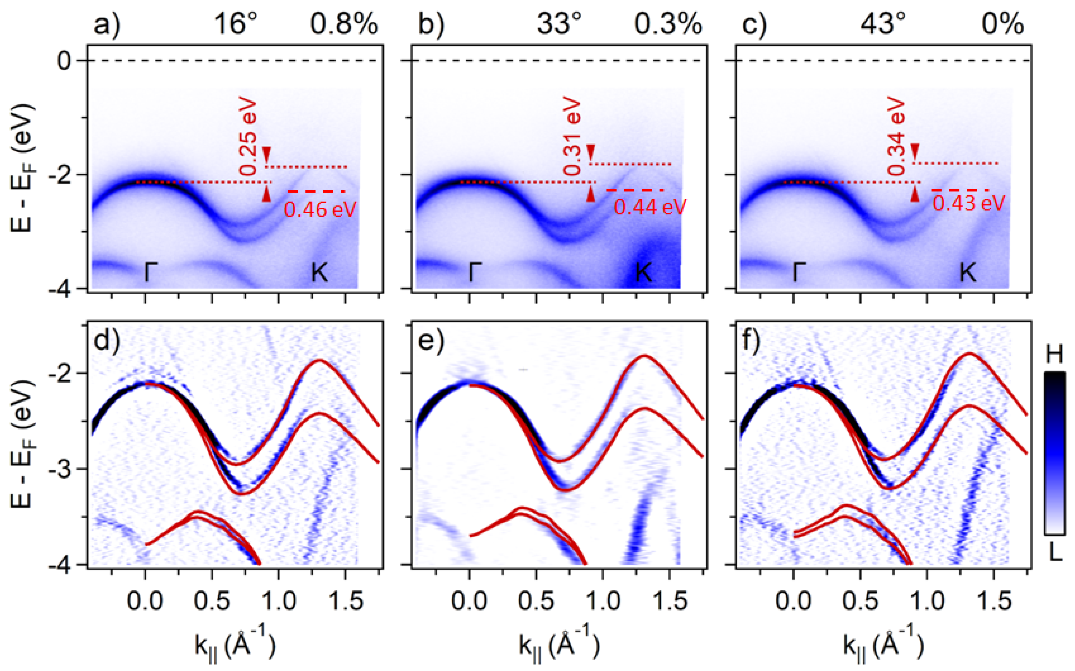
| Flake #3 | Flake #1 | Flake #2 | |
|---|---|---|---|
| WS2/Gr twist angle (°) | 16° | 33° | 43° |
| Valence ΔΓΚ difference (eV) | 0.25 | 0.31 | 0.34 |
| Computed biaxial strain (%) | +0.8 | +0.3 | 0.0 |
| Theoretical ΔSOC_theo (meV) at K | 440 | 434 | 430 |
| Experimental ΔSOC (meV) at K | 460 ± 5 | 440 ± 5 | 430 ± 5 |
Publisher’s Note: MDPI stays neutral with regard to jurisdictional claims in published maps and institutional affiliations. |
© 2021 by the authors. Licensee MDPI, Basel, Switzerland. This article is an open access article distributed under the terms and conditions of the Creative Commons Attribution (CC BY) license (https://creativecommons.org/licenses/by/4.0/).
Share and Cite
Ernandes, C.; Khalil, L.; Henck, H.; Zhao, M.-Q.; Chaste, J.; Oehler, F.; Johnson, A.T.C.; Asensio, M.C.; Pierucci, D.; Pala, M.; et al. Strain and Spin-Orbit Coupling Engineering in Twisted WS2/Graphene Heterobilayer. Nanomaterials 2021, 11, 2921. https://doi.org/10.3390/nano11112921
Ernandes C, Khalil L, Henck H, Zhao M-Q, Chaste J, Oehler F, Johnson ATC, Asensio MC, Pierucci D, Pala M, et al. Strain and Spin-Orbit Coupling Engineering in Twisted WS2/Graphene Heterobilayer. Nanomaterials. 2021; 11(11):2921. https://doi.org/10.3390/nano11112921
Chicago/Turabian StyleErnandes, Cyrine, Lama Khalil, Hugo Henck, Meng-Qiang Zhao, Julien Chaste, Fabrice Oehler, Alan T. Charlie Johnson, Maria C. Asensio, Debora Pierucci, Marco Pala, and et al. 2021. "Strain and Spin-Orbit Coupling Engineering in Twisted WS2/Graphene Heterobilayer" Nanomaterials 11, no. 11: 2921. https://doi.org/10.3390/nano11112921
APA StyleErnandes, C., Khalil, L., Henck, H., Zhao, M.-Q., Chaste, J., Oehler, F., Johnson, A. T. C., Asensio, M. C., Pierucci, D., Pala, M., Avila, J., & Ouerghi, A. (2021). Strain and Spin-Orbit Coupling Engineering in Twisted WS2/Graphene Heterobilayer. Nanomaterials, 11(11), 2921. https://doi.org/10.3390/nano11112921