
Atomic Layer Deposition of Ultrathin ZnO Films for Hybrid Window Layers for Cu(Inx,Ga1−x)Se2 Solar Cells

 , , ,
, , , 
Abstract
:
1. Introduction
2. Materials and Methods
2.1. Device Fabrication
2.2. ALD Process
2.3. Device Characterization
3. Results and Discussion
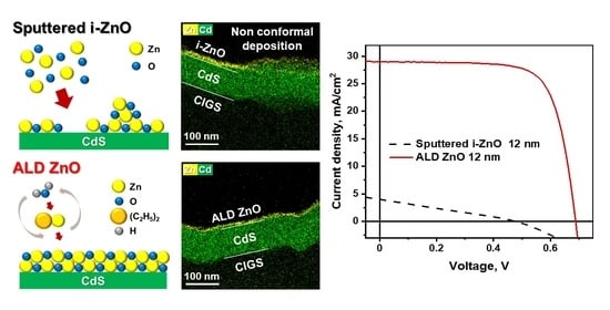
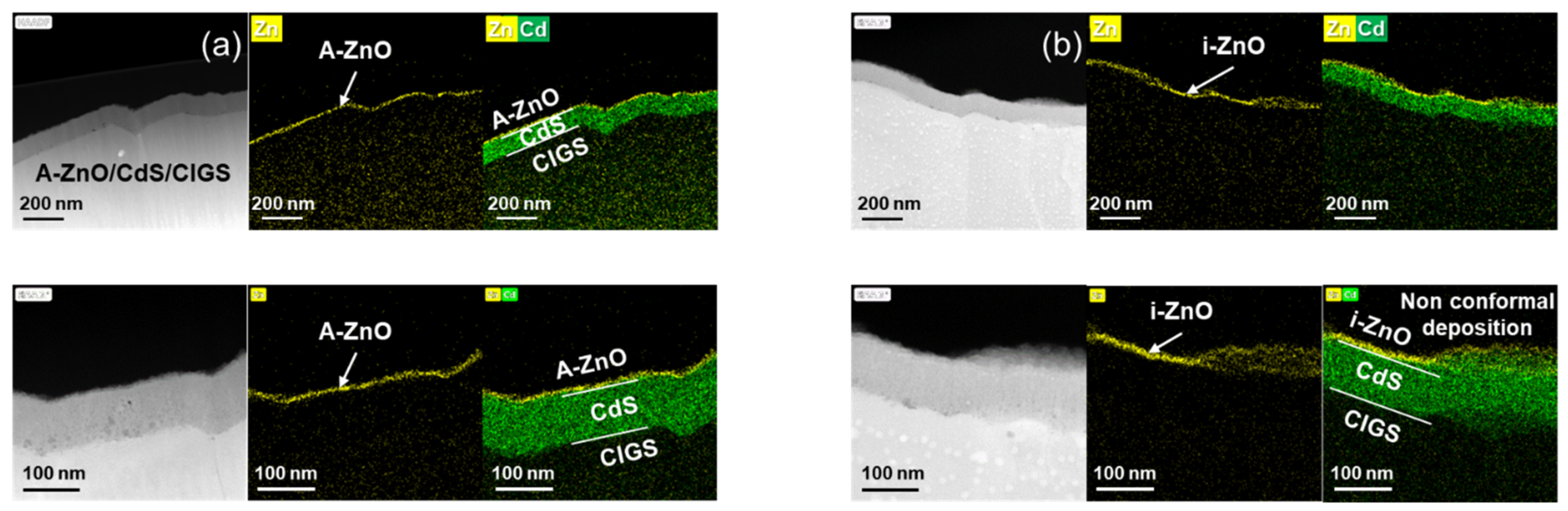
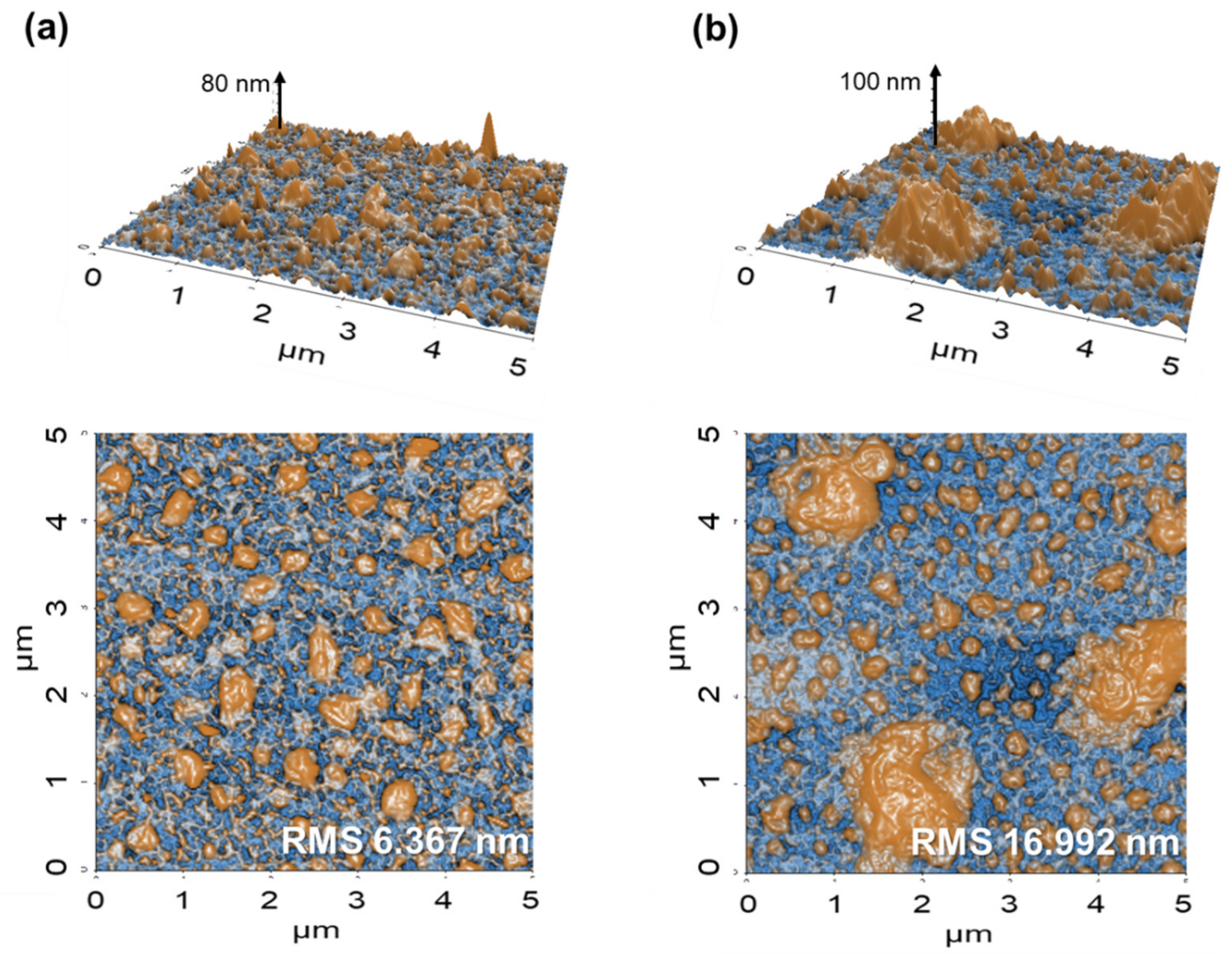
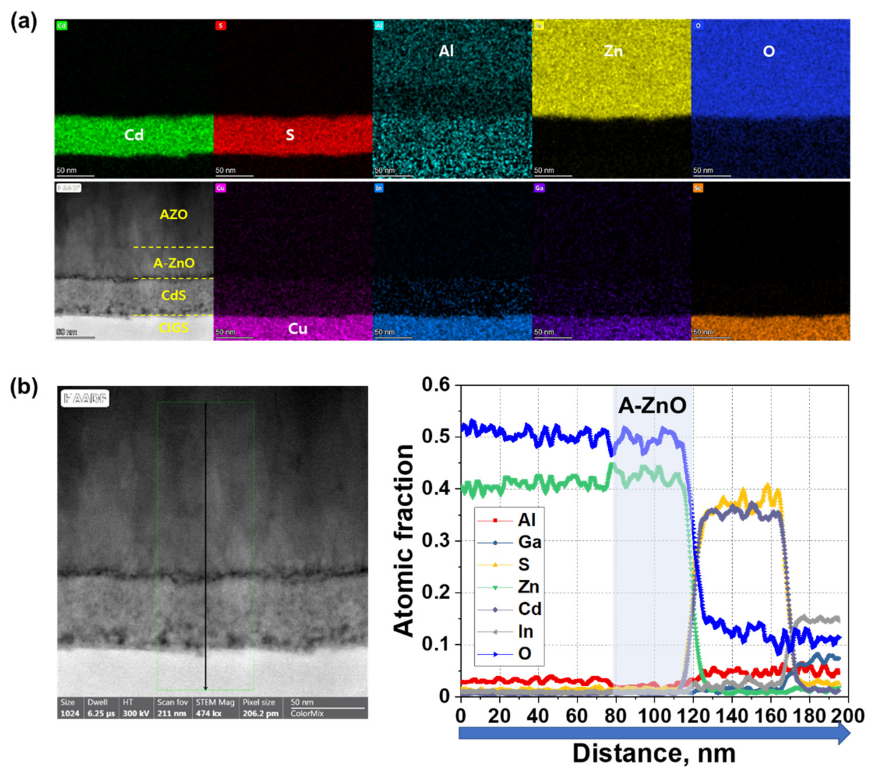
3.1. Formation of A-ZnO Window Layers on a CdS/CIGS Interface
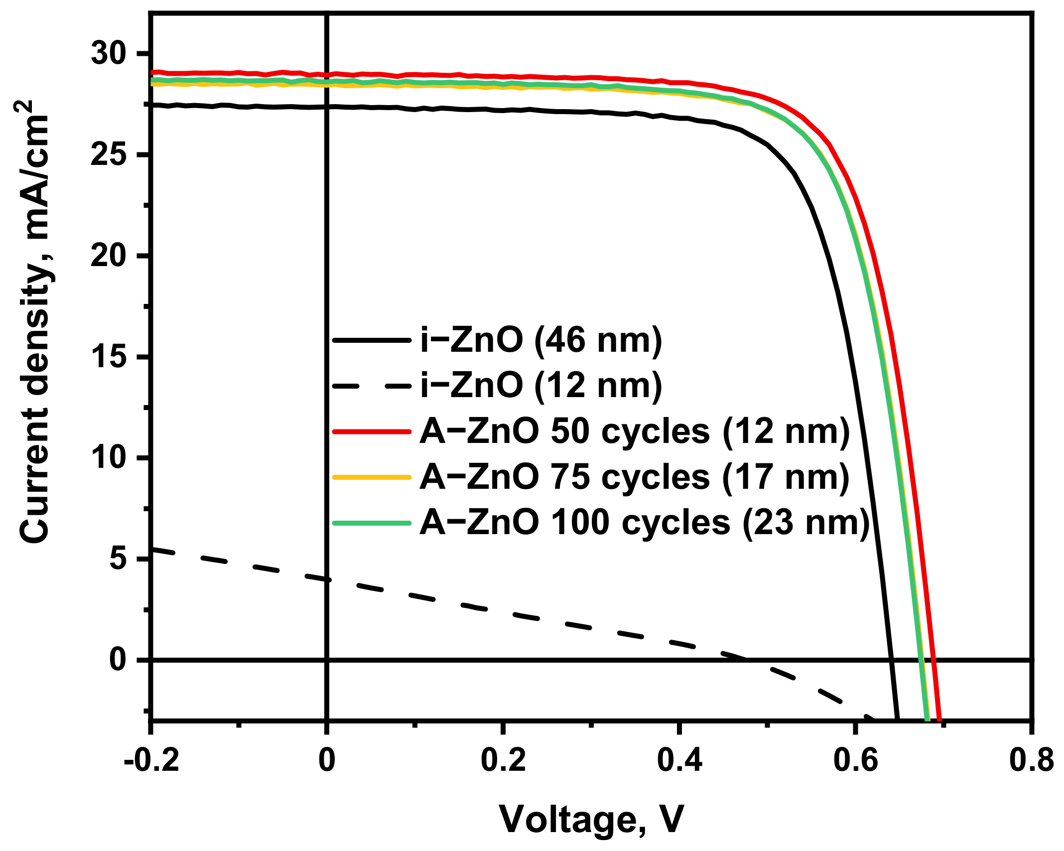
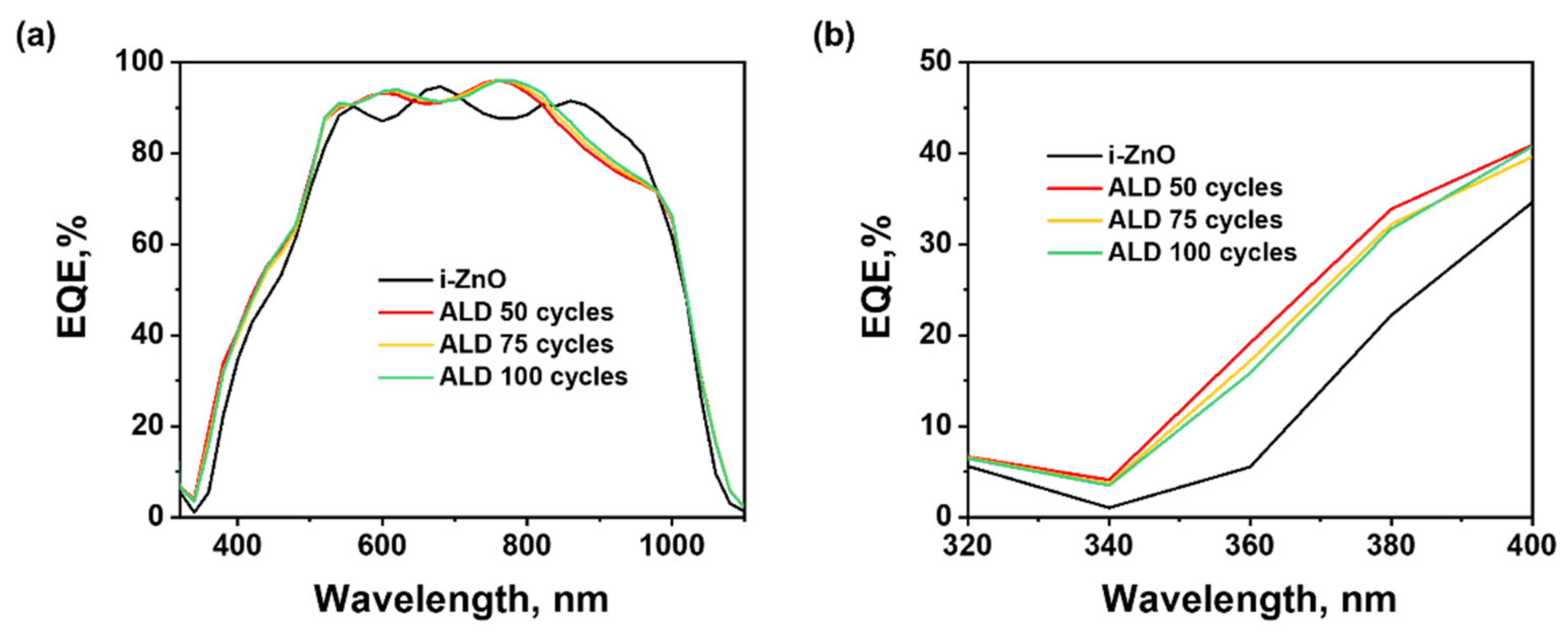
3.2. Performance of A-ZnO Window Layers in CIGS Solar Cells
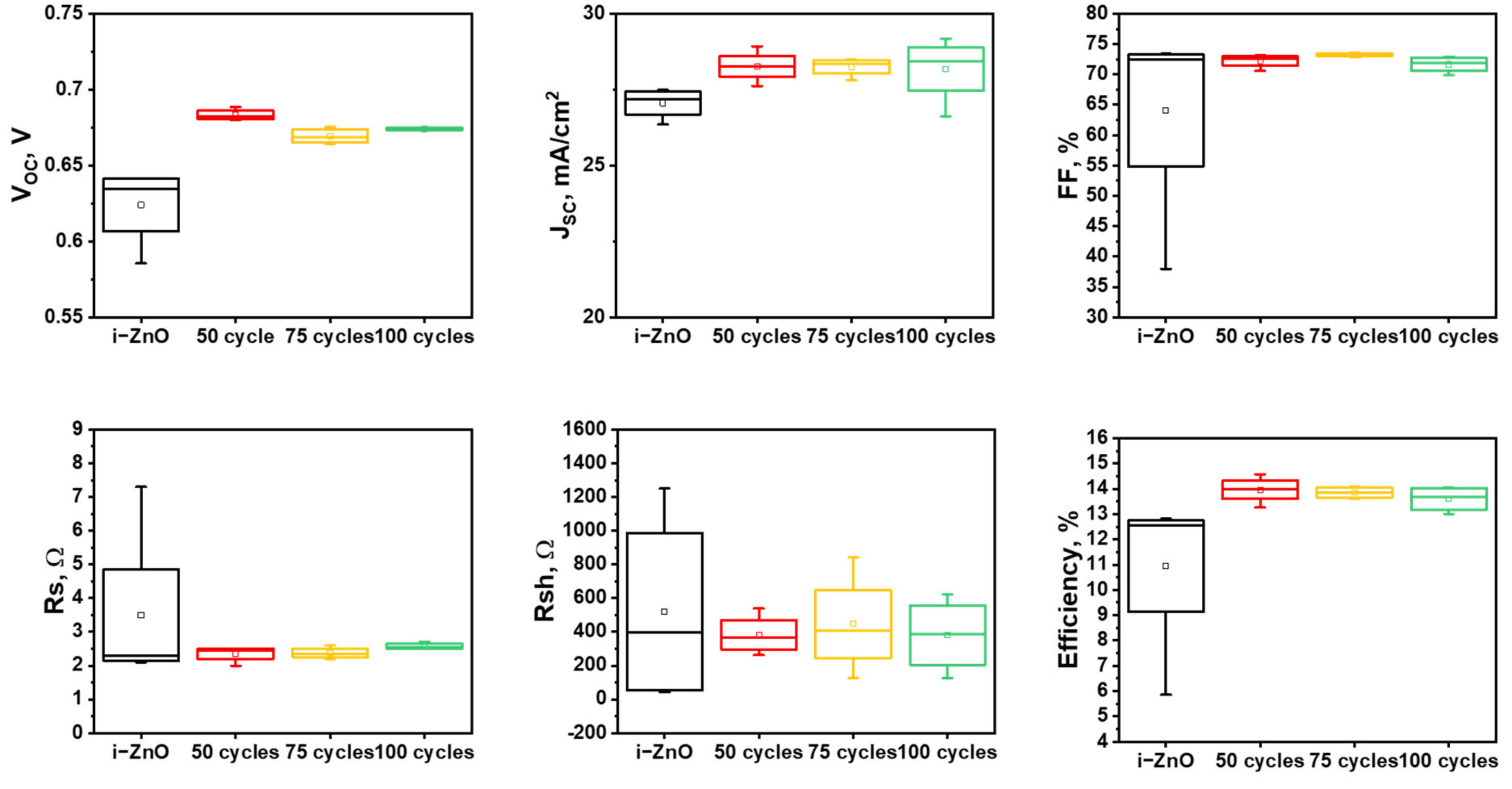
3.3. Effect of A-ZnO Window Layers on Photovoltaic Parameters
4. Conclusions
Supplementary Materials
Author Contributions
Funding
Institutional Review Board Statement
Informed Consent Statement
Data Availability Statement
Conflicts of Interest
References
- Chantana, J.; Kato, T.; Sugimoto, H.; Minemoto, T. Thin-film Cu(In,Ga)(Se,S)2 -based solar cell with (Cd,Zn)S buffer layer and Zn1−x Mg x O window layer. Prog. Photovolt. Res. Appl. 2017, 25, 431–440. [Google Scholar] [CrossRef]
- Kartopu, G.; Williams, B.; Zardetto, V.; Gürlek, A.; Clayton, A.; Jones, S.; Kessels, W.; Creatore, M.; Irvine, S. Enhancement of the photocurrent and efficiency of CdTe solar cells suppressing the front contact reflection using a highly-resistive ZnO buffer layer. Sol. Energy Mater. Sol. Cells 2018, 191, 78–82. [Google Scholar] [CrossRef]
- Jo, E.; Gil Gang, M.; Shim, H.; Suryawanshi, M.P.; Ghorpade, U.V.; Kim, J.H. 8% Efficiency Cu2ZnSn(S,Se)4 (CZTSSe) Thin Film Solar Cells on Flexible and Lightweight Molybdenum Foil Substrates. ACS Appl. Mater. Interfaces 2019, 11, 23118–23124. [Google Scholar] [CrossRef] [PubMed]
- Yago, A.; Sasagawa, S.; Akaki, Y.; Nakamura, S.; Oomae, H.; Katagiri, H.; Araki, H. Comparison of buffer layers on SnS thin-film solar cells prepared by co-evaporation. Phys. Status Solidi C 2017, 14, 1600194. [Google Scholar] [CrossRef]
- Williams, B.L.; Zardetto, V.; Kniknie, B.; Verheijen, M.A.; Kessels, W.M.; Creatore, M. The competing roles of i-ZnO in Cu(In,Ga)Se2 solar cells. Sol. Energy Mater. Sol. Cells 2016, 157, 798–807. [Google Scholar] [CrossRef]
- Nagoya, Y.; Sang, B.; Fujiwara, Y.; Kushiya, K.; Yamase, O. Improved performance of Cu(In,Ga)Se2-based submodules with a stacked structure of ZnO window prepared by sputtering. Sol. Energy Mater. Sol. Cells 2003, 75, 163–169. [Google Scholar] [CrossRef]
- Ishizuka, S.; Sakurai, K.; Yamada, A.; Matsubara, K.; Fons, P.; Iwata, K.; Nakamura, S.; Kimura, Y.; Baba, T.; Nakanishi, H.; et al. Fabrication of wide-gap Cu(In1−xGax)Se2 thin film solar cells: A study on the correlation of cell performance with highly resistive i-ZnO layer thickness. Sol. Energy Mater. Sol. Cells 2005, 87, 541–548. [Google Scholar] [CrossRef]
- Misic, B.; Pieters, B.E.; Theisen, J.P.; Gerber, A.; Rau, U. Shunt mitigation in ZnO:Al/i-ZnO/CdS/Cu(In,Ga)Se2 solar modules by the i-ZnO/CdS buffer combination. Phys. Status Solidi 2014, 212, 541–546. [Google Scholar] [CrossRef]
- Liu, W.-S.; Hsieh, W.-T.; Chen, S.-Y.; Huang, C.-S. Improvement of CIGS solar cells with high performance transparent conducting Ti-doped GaZnO thin films. Sol. Energy 2018, 174, 83–96. [Google Scholar] [CrossRef]
- Yu, X.; Ma, J.; Ji, F.; Wang, Y.; Zhang, X.; Cheng, C.; Ma, H. Preparation and properties of ZnO:Ga films prepared by RF magnetron sputtering at low temperature. Appl. Surf. Sci. 2005, 239, 222–226. [Google Scholar] [CrossRef]
- Macco, B.; Deligiannis, D.; Smit, S.; van Swaaij, R.A.C.M.M.; Zeman, M.; Kessels, W.M.M. Influence of transparent conductive oxides on passivation of a-Si:H/c-Si heterojunctions as studied by atomic layer deposited Al-doped ZnO. Semicond. Sci. Technol. 2014, 29, 122001. [Google Scholar] [CrossRef]
- Nandakumar, N.; Dielissen, S.B.; Garcia, D.D.G.-A.; Liu, Z.Z.; Gortzen, R.; Kessels, W.M.M.; Aberle, A.G.; Hoex, B. Resistive Intrinsic ZnO Films Deposited by Ultrafast Spatial ALD for PV Applications. IEEE J. Photovolt. 2015, 5, 1462–1469. [Google Scholar] [CrossRef]
- George, S.M. Atomic Layer Deposition: An Overview. Chem. Rev. 2009, 110, 111–131. [Google Scholar] [CrossRef] [PubMed]
- Knez, M.; Nielsch, K.; Niinistö, L. Synthesis and Surface Engineering of Complex Nanostructures by Atomic Layer Deposition. Adv. Mater. 2007, 19, 3425–3438. [Google Scholar] [CrossRef]
- Puurunen, R.L. Surface chemistry of atomic layer deposition: A case study for the trimethylaluminum/water process. J. Appl. Phys. 2005, 97, 121301. [Google Scholar] [CrossRef]
- Williams, B.L.; Smit, S.; Kniknie, B.J.; Bakker, K.J.; Keuning, W.; Kessels, W.M.M.; Schropp, R.E.I.; Creatore, M. Identifying parasitic current pathways in CIGS solar cells by modelling dark J-V response. Prog. Photovolt. 2015, 23, 1516–1525. [Google Scholar] [CrossRef] [Green Version]
- Arepalli, V.K.; Lee, W.-J.; Chung, Y.-D.; Kim, J. Growth and device properties of ALD deposited ZnO films for CIGS solar cells. Mater. Sci. Semicond. Process. 2021, 121, 105406. [Google Scholar] [CrossRef]
- Jahagirdar, A.H.; Kadam, A.A.; Dhere, N.G. Role of i-ZnO in Optimizing Open Circuit Voltage of CIGS2 and CIGS Thin Film Solar Cells. In Proceedings of the 2006 IEEE 4th World Conference on Photovoltaic Energy Conference, Waikoloa, HI, USA, 7–12 May 2006. [Google Scholar] [CrossRef]
- Tan, S.T.; Chen, B.J.; Sun, X.; Fan, W.J.; Kwok, H.S.; Zhang, X.H.; Chua, S.J. Blueshift of optical band gap in ZnO thin films grown by metal-organic chemical-vapor deposition. J. Appl. Phys. 2005, 98, 13505. [Google Scholar] [CrossRef] [Green Version]
- Guziewicz, E.; Godlewski, M.; Krajewski, T.; Wachnicki, L.; Szczepanik, A.; Kopalko, K.; Wójcik-Głodowska, A.; Przeździecka, E.; Paszkowicz, W.; Łusakowska, E.; et al. ZnO grown by atomic layer deposition: A material for transparent electronics and organic heterojunctions. J. Appl. Phys. 2009, 105, 122413. [Google Scholar] [CrossRef]

| Thickness (nm) | VOC (V) | JSC (mA/cm2) | FF (%) | Efficiency (%) | Rs (Ω) | Rsh (Ω) | |
|---|---|---|---|---|---|---|---|
| i-ZnO (Ref.) | 46 | 0.64068 | 27.3669 | 73.0578 | 12.809 | 2.4 | 723.6 |
| i-ZnO | 12 | 0.47154 | 14.0397 | 25.9519 | 1.736 | 16.4 | 66.8 |
| A-ZnO (50 cycles) | 12 | 0.68862 | 28.9264 | 73.1868 | 14.578 | 2.0 | 539.3 |
| A-ZnO (75 cycles) | 17 | 0.67545 | 28.4352 | 73.2842 | 14.075 | 2.6 | 365.8 |
| A-ZnO (100 cycles) | 23 | 0.67429 | 28.5909 | 72.9267 | 14.059 | 2.6 | 490.5 |
| Mobility (cm2/V⋅s) | Conductivity (1/Ω⋅cm) | Resistivity (Ω⋅cm) | Carrier Concentration (cm−3) | |
|---|---|---|---|---|
| Sputtered i-ZnO | 14.77 | 7.684 × 10⁻⁶ | 1.301 × 10⁵ | −3.247 × 10¹² |
| A-ZnO | 12.99 | 14.59 | 6.852 × 10⁻² | −7.015 × 10¹⁸ |
Publisher’s Note: MDPI stays neutral with regard to jurisdictional claims in published maps and institutional affiliations. |
© 2021 by the authors. Licensee MDPI, Basel, Switzerland. This article is an open access article distributed under the terms and conditions of the Creative Commons Attribution (CC BY) license (https://creativecommons.org/licenses/by/4.0/).
Share and Cite
Lee, J.; Jeon, D.-H.; Hwang, D.-K.; Yang, K.-J.; Kang, J.-K.; Sung, S.-J.; Park, H.; Kim, D.-H. Atomic Layer Deposition of Ultrathin ZnO Films for Hybrid Window Layers for Cu(Inx,Ga1−x)Se2 Solar Cells. Nanomaterials 2021, 11, 2779. https://doi.org/10.3390/nano11112779
Lee J, Jeon D-H, Hwang D-K, Yang K-J, Kang J-K, Sung S-J, Park H, Kim D-H. Atomic Layer Deposition of Ultrathin ZnO Films for Hybrid Window Layers for Cu(Inx,Ga1−x)Se2 Solar Cells. Nanomaterials. 2021; 11(11):2779. https://doi.org/10.3390/nano11112779
Chicago/Turabian StyleLee, Jaebaek, Dong-Hwan Jeon, Dae-Kue Hwang, Kee-Jeong Yang, Jin-Kyu Kang, Shi-Joon Sung, Hyunwoong Park, and Dae-Hwan Kim. 2021. "Atomic Layer Deposition of Ultrathin ZnO Films for Hybrid Window Layers for Cu(Inx,Ga1−x)Se2 Solar Cells" Nanomaterials 11, no. 11: 2779. https://doi.org/10.3390/nano11112779
APA StyleLee, J., Jeon, D.-H., Hwang, D.-K., Yang, K.-J., Kang, J.-K., Sung, S.-J., Park, H., & Kim, D.-H. (2021). Atomic Layer Deposition of Ultrathin ZnO Films for Hybrid Window Layers for Cu(Inx,Ga1−x)Se2 Solar Cells. Nanomaterials, 11(11), 2779. https://doi.org/10.3390/nano11112779