Article

Theoretical Analysis of Terahertz Dielectric–Loaded Graphene Waveguide

1
College of Physics and Electronic Engineering, Zhengzhou Normal University, Zhengzhou 450044, China
2
Key Laboratory of Infrared Imaging Materials and Detectors, Shanghai Institute of Technical Physics, Chinese Academy of Sciences, Shanghai 200083, China
*
Author to whom correspondence should be addressed.
Nanomaterials 2021, 11(1), 210; https://doi.org/10.3390/nano11010210
Submission received: 12 December 2020 / Revised: 10 January 2021 / Accepted: 12 January 2021 / Published: 15 January 2021
(This article belongs to the Special Issue Low-Dimensional Nanomaterials for Photonics and Optoelectronics)

Abstract

:
The waveguiding of terahertz surface plasmons by a GaAs strip-loaded graphene waveguide is investigated based on the effective-index method and the finite element method. Modal properties of the effective mode index, modal loss, and cut-off characteristics of higher order modes are investigated. By modulating the Fermi level, the modal properties of the fundamental mode could be adjusted. The accuracy of the effective-index method is verified by a comparison between the analytical results and numerical simulations. Besides the modal properties, the crosstalk between the adjacent waveguides, which determines the device integration density, is studied. The findings show that the effective-index method is highly valid for analyzing dielectric-loaded graphene plasmon waveguides in the terahertz region and may have potential applications in subwavelength tunable integrated photonic devices.

Graphical Abstract

1. Introduction

The terahertz (THz) wave, usually defined as a frequency ranging from 1 to 10 THz, has attracted numerous research interests due to its potential applications in the fields of spectroscopy, imaging, defense industries, on-chip communications [1,2,3,4,5,6], etc. In particular, guiding the THz wave is a challenge for applications in communications; thus, the THz waveguide has become a hot research topic. By using THz waveguides, THz waves can be easily concentrated in the subwavelength region, offering a tightly confined modal field beyond the diffraction limit [7]. Earlier, dielectric waveguides [8,9,10,11] and noble metal-based structures [12,13,14,15,16,17,18,19,20,21,22,23,24,25] were widely investigated for THz waveguiding, such as hollow-core [10] and porous-core dielectric waveguides [11], metallic nanowires [13,14,15,16,17,18,19,20,21,22,23,24,25], metal-based hybrid waveguides [26,27,28], etc. THz dielectric waveguides could realize a low loss mode propagation; however, the modal fields are diffraction-limited. In contrast to dielectric waveguides, metallic waveguides could support the transverse magnetic (TM) surface plasmon (SP) mode [29], while in the THz range, the SP effects of metal are relatively weak [30], thus hindering the applications at a subwavelength scale.
Recently, it was reported that graphene could also excite SP modes [31,32,33] in the infrared band, offering an alternative approach to guiding THz waves. Compared with the metallic waveguides, graphene plasmon waveguides could confine the infrared waves into the deep subwavelength scale, and the guided modes could be easily tuned [34]. Up to now, lots of graphene-based configurations have been proposed to guide the infrared waves, such as graphene ribbons [35], graphene slot waveguides [36,37], graphene wedge and groove waveguides [38], dielectric-loaded graphene waveguides [39], graphene-coated nanowires [40,41,42,43,44,45,46], graphene-based hybrid waveguides [47,48], etc.
In the THz band, Huang et al. [49] proposed a graphene-coated nanowire with a drop-shaped cross section to realize low loss waveguiding with an ultra-strong mode confinement. Additionally, a graphene-coated elliptical nanowire was suggested for ultra-deep subwavelength THz waveguiding [50]. Zhou et al. [51] proposed a graphene-based hybrid plasmonic waveguide to achieve ultra-deep subwavelength modal field confinement. A symmetric hybrid plasmonic waveguide [52] was proposed to achieve a propagation length of 26.7 mm and mode area of about 4 μm2 at 10 THz. Later, Wan et al. [53] proposed a dielectric-loaded graphene groove waveguide, and a typical propagation length of about 37.8 μm and mode area of about 52 μm2 were obtained at 1.5 THz. To achieve a better modal field confinement, two graphene-based hybrid plasmonic waveguides were proposed [54,55], which could simultaneously achieve an ultra-small modal area and a propagation length of about several hundreds of micrometers at 3 THz. Despite recent progress in graphene-based waveguides, we note that the current reports mainly focus on the near- and mid-infrared band, and graphene-based THz waveguides are studied less, relatively speaking. Furthermore, to the best of our knowledge, the modal properties and crosstalk in dielectric-loaded graphene surface plasmon waveguides (DLGSPWG) have not yet been fully investigated in the THz region.
In this paper, we extend the concept of the dielectric-loaded plasmon waveguide [39,56,57,58], which dates back to 2006, from the near- and mid-infrared band to the THz band by proposing a THz DLGSPWG. Although the physics behind this are similar to those of [39,58], our findings show something new. The DLGSPWG could be easily fabricated, and the substrate structures can provide additional freedom to tune the modal properties. Based on the effective-index method (EIM) [58,59,60], we first give an approximate analytical model for the DLGSPWG and then calculate the effective mode index, propagation length, and the cut-off wavelength of higher order modes. The group velocity of the propagated modes and crosstalk between adjacent structures are also discussed. Our findings show that the EIM is highly valid for analyzing DLGSPWG in the THz region, and the results are verified by the numerical simulations based on the finite element method (FEM). The results also show that the electromagnetic field in the corner regions is only partly responsible for the difference between the EIM and FEM results and that the crosstalk between adjacent structures is negligible even at a very small separation distance.

2. Theory

As seen from Figure 1a, the proposed DLGSPWG consists of a GaAs dielectric strip with a width of w and height of h located on the graphene layer above a semi-infinite dielectric substrate. Figure 1b,c show the equivalent four- and three-layer a structures considered in the EIM. The relative permittivities of the GaAs strip (ε2) and substrate (ε1) are set to be 12.25 [54,55]. The range of frequency is from 2 to 10 THz.
We first employ EIM to give an approximate analytical model for the DLGSPWG and then verify the results by using the FEM simulation. In the EIM, the 2D cross-section of the DLGSPWG is divided into two 1D waveguide structures (Figure 1b,c). By individually solving the guided modes of these two 1D waveguides [58], one can finally obtain the guided modes of the DLGSPWG. The proposed DLGSPWG (Figure 1a) could be obtained by narrowing the width of the top GaAs dielectric layer (Figure 1b). Then, we can calculate the effective mode index nco of the guided modes in such an equivalent four-layer structure. All the dimensions are infinite along the x axis, and the upper air and substrate dielectric layers are semi-infinite along the y direction. Here, nco is irrelevant to the width of the dielectric strip and is equivalent to that of the effective mode index of the SP mode supported by the air-dielectric-graphene-dielectric structure (Figure 1b), which is given as [31] n co = ε 0 ( ε 1 + ε 2 ) c i / σ g , where ε0 is the permittivity in air, σg is the optical conductivity of graphene, and c is the speed of light. Then, the GaAs strip serves as the core of a three-layer dielectric waveguide shown in Figure 1c. The effective mode index ncl is equivalent to that of the SP mode supported by the graphene-air interface and is given by [31] n cl = ε 0 ( ε 1 + 1 ) c i / σ g . Finally, the eigen-equation of the equivalent dielectric planar waveguide for the N-th order guided transverse electric (TE) mode (i.e., TM plasmon mode) is given as [56]:
tan ( k 1 w N π 2 ) = k 2 / k 1 , N = 0 , 1 , 2
where k 1 = k 0 n co 2 n neff 2 , k 2 = k 0 n neff 2 n cl 2 , k0 = 2π/λ0, λ0 is the wavelength of incident light in free space. w is the width of the dielectric strip, and neff is the effective mode index of the propagating modes in DLGSPWG. By numerically solving Equation (1), the effective mode index neff of the N-th order mode could be obtained. The real part of neff is related to the dispersion, and the imaginary part Im(neff) is related to the modal loss. The power propagation length LP is defined as LP = 1/2α, where α is the loss factor related to Im(neff) and given by α = k0Im(neff). Therefore, the power propagation length could be calculated by LP = λ0/[4πIm(neff)]. The cut-off condition of the guided modes is k2 = 0. Then, the cut-off wavelength of the N-th order guided mode can be calculated by [58,60]:
N λ cutoff N = 2 w Re ( n co 2 n cl 2 ) ,   N = 1 , 2 , 3
Here, the impact of the strip height h (assumed to be infinite) has not been taken into account in the EIM, since graphene plasmons are tightly concentrated at the interface of the graphene layer. In the FEM calculation, the height of the dielectric strip is h = 2 μm, which is enough to guarantee the accuracy. Furthermore, enlarging h will be much closer to the situation in EIM and will lead to a better match between the EIM and FEM results, especially for the fundamental mode. We will show this subsequently.
In the calculation, the graphene layer is modelled as an electric field-induced surface current J = σgE on the surface of the substrate, thus neglecting the thickness of the graphene layer. Within the random-phase approximation, the complex optical conductivity of graphene [61,62,63] consists of the interband and intraband contributions in the THz range, that is σg = σintra + σinter, with:
σ intra = 2 i e 2 k B T π ħ 2 ( ω + i / τ ) ln [ 2 cosh ( E F 2 k B T ) ]
σ inter = e 2 4 ħ [ 1 2 + 1 π arctan ( ħ ω 2 E F 2 k B T ) i 2 π ln ( ħ ω + 2 E F ) 2 ( ħ ω 2 E F ) 2 + ( 2 k B T ) 2 ]
Here, we set τ = 0.5 ps (unless otherwise mentioned) for the electron relaxation time and T = 300 K for the temperature. EF is the Fermi energy level of the graphene, ω is the angular frequency of incident light, ħ is the reduced plank constant, kB is the Boltzmann’s constant, and e is the charge of the electron.
The FEM results are obtained by use of the wave optics module of COMSOL Multiphysics. The eigenvalue solver is used to find modes of the waveguide. The calculation domain is 2λ0 × 2λ0, and a perfectly matched layer (PML) is applied around the geometry to avoid the influence of reflection. A convergence analysis is also conducted to ensure that the numerical boundaries and meshing do not interfere with the solutions.
In the derivation of Equation (1), we assume that graphene can support and propagate TM plasmon modes. Actually, graphene can support TM plasmon modes when Im(σg) > 0 [32]. To illustrate this, we plot σg with respect to the frequency and EF in Figure 2. Obviously, within the frequency region (2–10 THz, i.e., corresponding wavelength region 30–150 μm) and Fermi energy level region considered here, the imaginary parts of σg (Im(σg) = σi) are always above zero, thus indicating that TM plasmon modes could be excited.

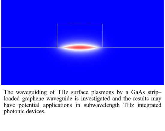
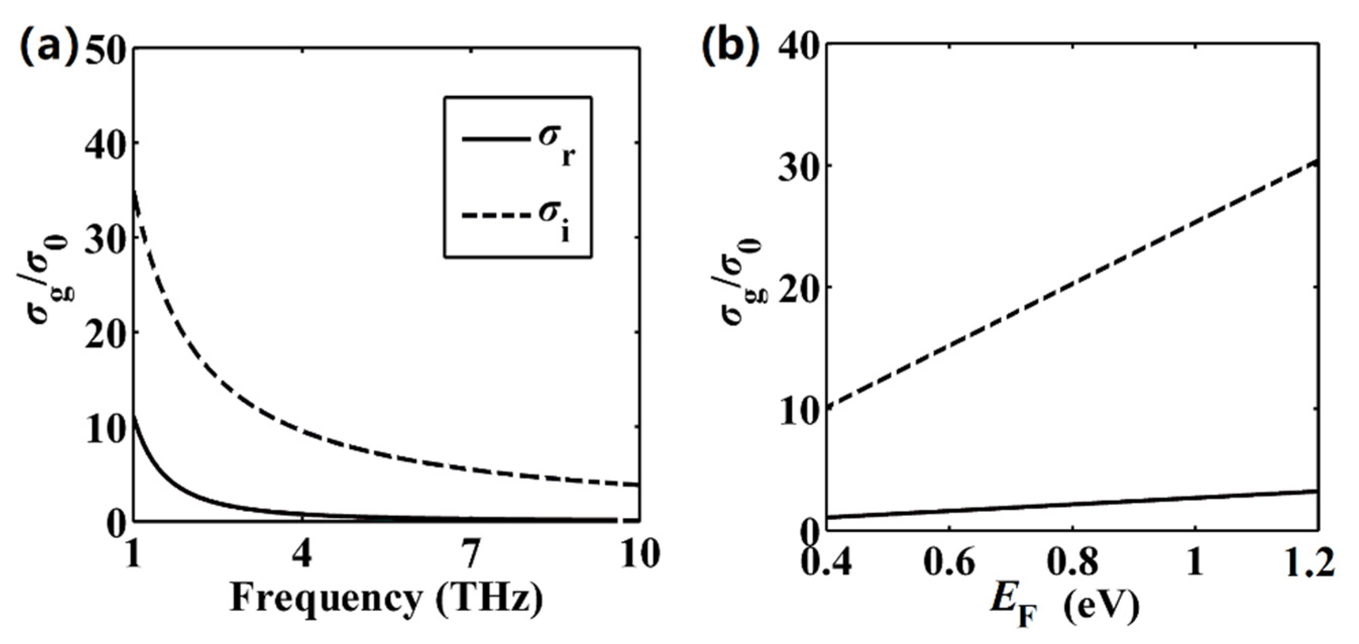
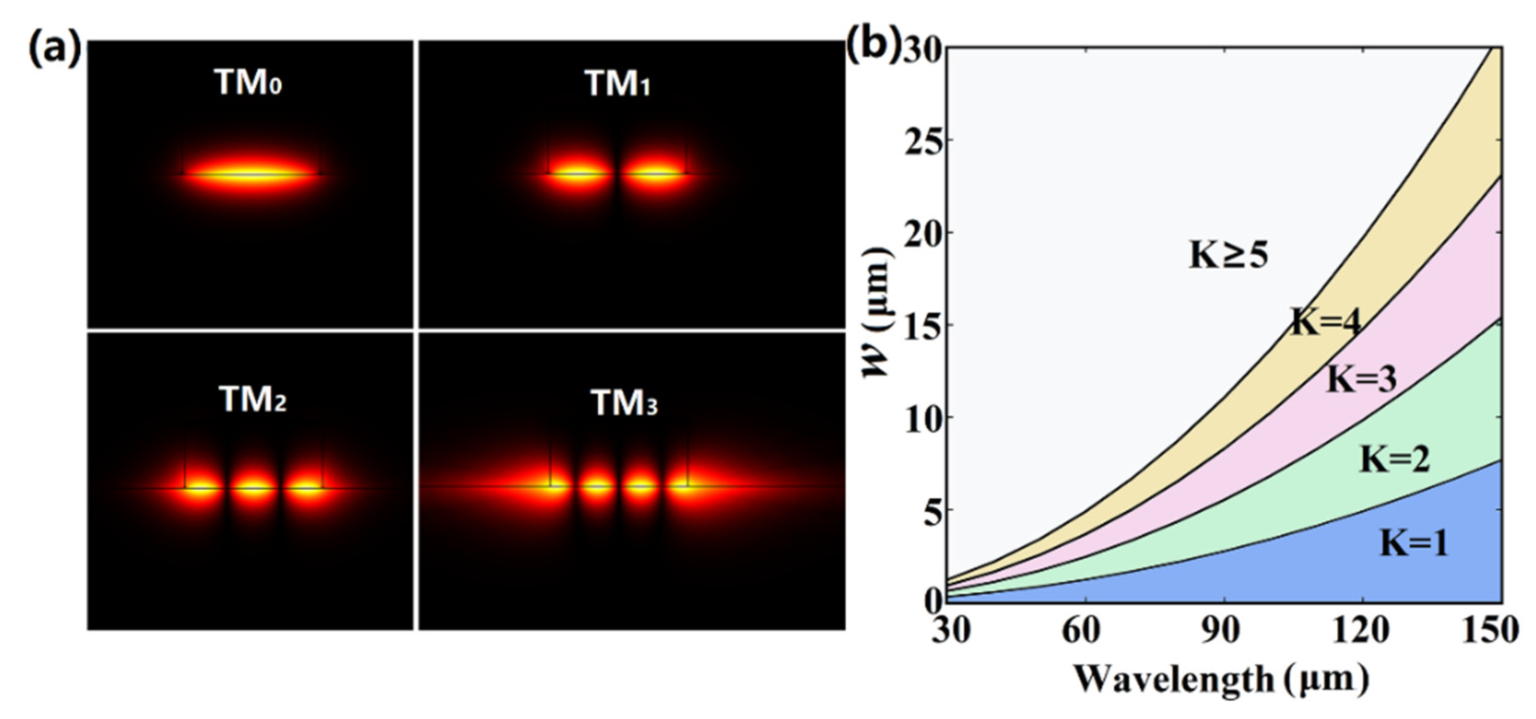
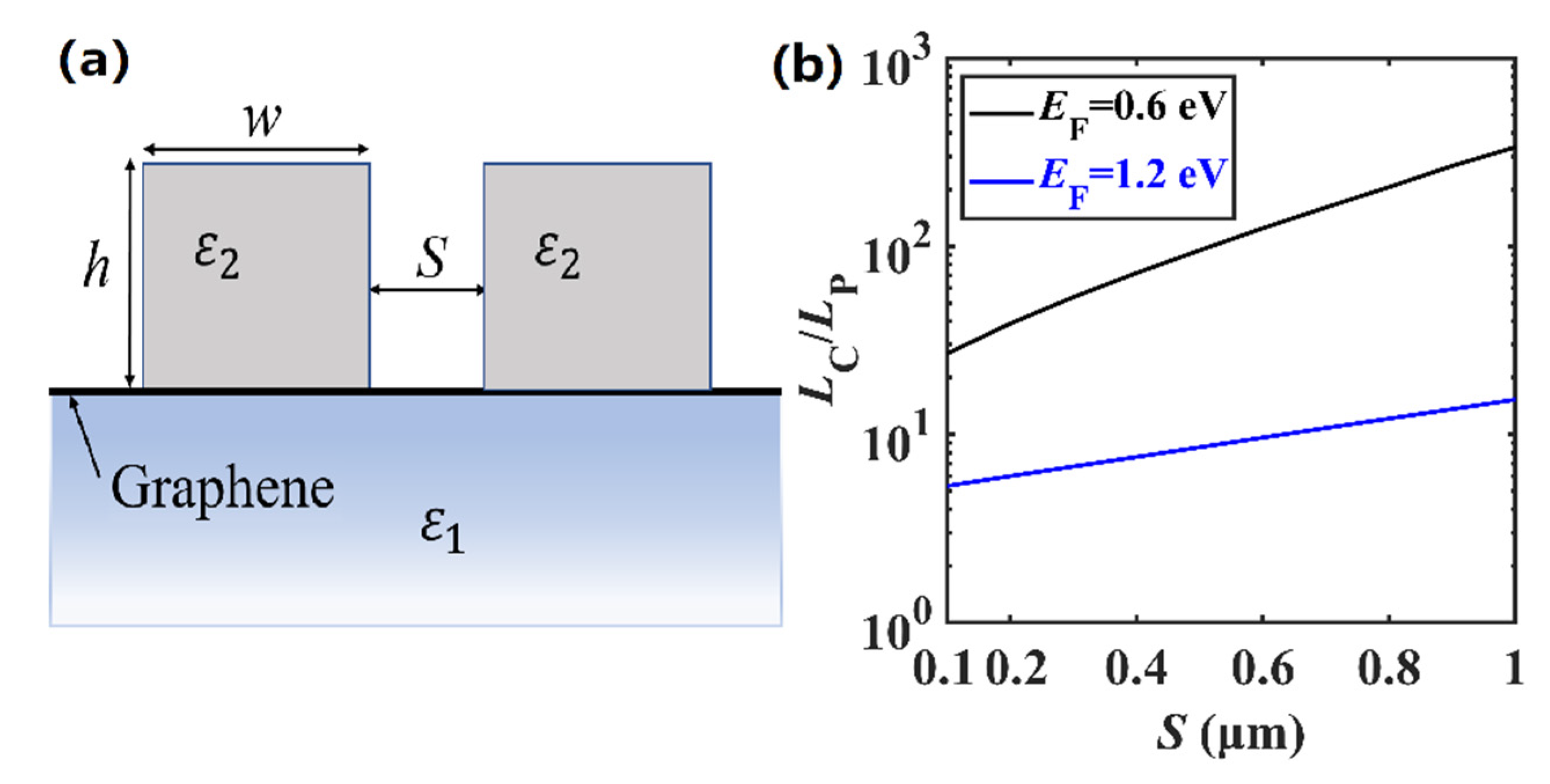
3. Results and Discussion

By analytically solving Equation (1), we first investigate the effective mode indices of the SP modes supported by the DLGSPWG, and then verify the analytical results by using the FEM simulation. In the calculation, the width and height of the dielectric strip are w = 4 μm and h = 2 μm. As seen from Figure 3, the EIM results (symbols) are in good agreement with the FEM (solid lines) results when the wavelength is smaller than the cut-off wavelength. The fundamental plasmon mode (N = 0, TM0) has a larger real part of the effective mode index (Re(neff)) than the higher order modes (N = 1, 2, 3), which implies a shorter wavelength (λSP = λ0/Re(neff)), as shown in Figure 3a. All the mode indices are located between nco and ncl. When increasing the wavelength from 30 to 150 μm, Re(neff) decreases monotonically and the higher order modes are gradually cut off. The power propagation length increases monotonically, which suggests a smaller modal loss at longer wavelengths (Figure 3b).
As the wavelength is close to the cut-off wavelength, the EIM results show slight deviations from the FEM results. This is due to the fact that the electromagnetic fields in the corner regions have not been taken into account in the EIM. At shorter wavelengths, the modal fields are perfectly localized in the GaAs strip. Therefore, the EIM results are highly consistent with the FEM simulation results. Figure 4a shows the modal fields (|Ey|) of the first four order modes at the wavelength of 60 μm (5 THz), and one can see that the fields are perfectly localized below the GaAs strip. However, at longer wavelengths, the modal fields are not perfectly localized, which leads to slight difference between these two methods.
The fundamental plasmon mode is cut-off-free and has a lower modal loss compared with higher order modes and could thus be used for long-range propagation. Here, the waveguide could also support higher order modes, and we next study the single and multi-mode operation regions by solving Equation (2). As shown in Figure 4b, at a certain wavelength the numbers of guided modes (K) increase with an increasing width of the GaAs strip. The critical values of w for the single-mode operation are 0.3073 μm and 7.6937 μm for λ0 = 30 and 150 μm, respectively. As w increases, the single-mode operation region tends towards a longer wavelength. At a certain width, the number K decreases with an increase in the wavelength. Finally, single mode propagation could be achieved at a very small w and long wavelength.
As depicted in Figure 3, the EIM results (symbols) are in very good agreement with the FEM (solid lines) results when the wavelength is smaller than 120 μm. Therefore, the wavelength ranges from 30 to 120 μm (i.e., 2.5–10 THz) in what follows.
In Section 2, it is mentioned that the impact of the strip height h (assumed to be infinite) has not been taken into account in the EIM, while in the FEM calculation the height of the dielectric strip is h = 2 μm. To make the structure used in the numerical simulation much closer to that used in EIM, we have studied the effective mode indices with respect to the wavelength at different strip heights h for the TM0 and TM1 modes, as shown in Figure 5. We find that the electromagnetic field in the corner regions is only partly responsible for the difference between the EIM and FEM results. By enlarging h, these two results are in better agreement with each other, even at longer wavelengths. As seen from Figure 5, the FEM results with a larger strip height (blue (h = 4 μm) and black lines (h = 8 μm)) have smaller deviations compared with the EIM results (symbols) for the TM0 mode. For instance, when h = 2 μm and the wavelength is 120 μm, the relative deviation of Re(neff) between FEM and EIM is about 9.9%, while the relative deviation is only 2.7% for h = 8 μm. As for the imaginary parts of neff, the relative deviation is always less than 6%. Interestingly, the strip height seems to have little effect on the effective mode indices for the TM1 mode, and the EIM results are always in good agreement with the FEM results, even at different h values.
Next, we study the group velocity, defined as v g = ω / ( k 0 n eff ) , of the propagated THz plasmon modes. As shown in Figure 6, the group velocity of the TM0 mode gradually decreases with an increasing frequency, which is due to the fact that Re ( n eff ) + ω Re ( n eff ) / ω (that is, c / v g ) is much larger at a higher frequency. As for the TM1 mode, the group velocity first rapidly decreases and then approaches that of TM0. One can see that the EIM results are consistent with the FEM results.
One of the outstanding properties of graphene is the tunability of the surface conductivity by employing a DC bias [64], and this therefore provides us with a feasible method for modulating the effective mode indices of the guided modes. Figure 7 shows the effective mode indices of the fundamental mode in DLGSPWG with respect to the wavelength at different EF values. As we have mentioned above, one could get a better fitting between the FEM and EIM results by enlarging the strip height at longer wavelengths. Hence, h is set to be 8 μm. The carrier density in graphene could reach a value as high as 1014 cm−2 [65], and the corresponding EF is about 1.17 eV. In a relatively recent work [66], the Fermi energy level reached a value as high as 1.77 eV. Here, EF varies from 0.6 eV to 1.2 eV. It is worth mentioning that we set τ = 0.5 ps in the above investigations. Actually, τ is related to EF and is given by τ = nEF/eVF2 [67,68], where n = 10,000 cm2/(V·s) is the carrier mobility of graphene and VF = 106 m·s−1. As a result, τ is 0.9 (1.2) ps for EF = 0.9 (1.2) eV. From Figure 7a, one can see that at a fixed wavelength, Re(neff) decreases as EF increases. For EF = 0.9 eV, the analytical results of Re(neff) range from 38.49 to 7.24. Clearly, the EIM results are in good agreement with the FEM results. In terms of the imaginary parts, shown in Figure 7b, when enlarging EF, Im(neff) decreases dramatically, which is due to the fact that the interband contribution of σg is reduced by increasing the Fermi energy level. Thus, the propagation length could be massively enhanced. However, the EIM results show a slight discrepancy with the FEM results at longer wavelengths. This is because the electromagnetic fields in the corner regions have not been taken into account in the EIM; thus, the modal loss is slightly larger than for the FEM results.
Besides the modal properties, crosstalk between the adjacent waveguides, which determines the device integration density, is also an important factor in subwavelength photonic integration. In order to investigate the crosstalk, we set a coupling system with two DLGSPWG structures separated by a distance of S, as shown in Figure 8a. To evaluate the performance of the coupling system in the integrated THz circuit, crosstalk is characterized by using a coupling length LC [69], which is calculated by LC = π/(|βsβas|), based on the coupled mode theory [69], where βs = k0neff,s and βas = k0neff,as are the complex propagation constants of the symmetric and antisymmetric modes at 5 THz, respectively. Figure 8b shows the normalized coupling length LC/LP with respect to S. The dependence of the coupling length LC on S indicates that the crosstalk would be weaker with the increase of S. To ensure a very low crosstalk, LC/LP needs to be large enough (usually exceeding 10). This means that the energy of the mode decays to 1/e of its original value before it is coupled to the adjacent structure; thus, the crosstalk between adjacent structures is negligible. Here, even at a very small separation distance of S = 0.1 μm, LC/LP is as high as 26.89 for EF = 0.6 eV; thus, the crosstalk can almost be ignored. However, for EF = 1.2 eV, LC/LP is about 10 for S = 0.6 μm. The low-mode crosstalk between the adjacent waveguides shows its potential application in ultra-compact and high-density integration.

4. Conclusions

We extend the concept of dielectric-loaded plasmon waveguide from the near- and mid-infrared band to the THz band. The SP modes of the DLGSPWG are studied by using the EIM and FEM. The tunability of the fundamental mode, effective mode index, propagation length, and the cut-off wavelength of higher order modes are investigated. The EIM results are in good agreement with the FEM results in the THz band. Our findings show that the electromagnetic field in the corner regions is only partly responsible for the difference between the EIM and FEM results. Enlarging the strip height will lead to a better fitting between the EIM and FEM results, especially for the fundamental mode. Besides this, we show that the DLGSPWG shows very small crosstalk between the adjacent structures, even at a very small separation distance of 0.1 μm. The DLGSPWG may have potential applications in tunable subwavelength terahertz photonic devices.

Author Contributions

Conceptualization, D.T.; writing—original draft preparation, D.T.; writing—review and editing, K.W.; visualization, K.W.; supervision, D.T., K.W. All authors have read and agreed to the published version of the manuscript.

Funding

This work was supported by the China Postdoctoral Science Foundation (2020M671247), Key Scientific Research Project of Henan College (21A140029), Young Backbone Teacher Training Program of Zhengzhou Normal University (QNGG-20774), Open Research Fund of Zhengzhou Normal University, Scientific Research Starting Foundation of Zhengzhou Normal University.

Institutional Review Board Statement

Not applicable.

Informed Consent Statement

Not applicable.

Data Availability Statement

The data presented in this study are available on request from the corresponding author.

Acknowledgments

The authors would like to acknowledge Minning Zhu from Rutgers, the State University of New Jersey for useful discussions.

Conflicts of Interest

The authors declare no conflict of interest.

References

  1. Ahmadivand, A.; Gerislioglu, B.; Ahuja, R.; Mishra, Y.K. Terahertz plasmonics: The rise of toroidal metadevices towards immunobiosensings. Mater. Today 2020, 32, 108–130. [Google Scholar] [CrossRef]
  2. Chan, W.L.; Deibel, J.; Mittleman, D.M. Imaging with terahertz radiation. Rep. Prog. Phys. 2007, 70, 1325–1379. [Google Scholar] [CrossRef]
  3. Ma, J.; Shrestha, R.; Adelberg, J.; Yeh, C.Y.; Hossain, Z.; Knightly, E.; Jornet, J.M.; Mittleman, D.M. Security and eavesdropping in terahertz wireless links. Nature 2018, 563, 89–93. [Google Scholar] [CrossRef] [PubMed]
  4. Koenig, S.; Lopez-Diaz, D.; Antes, J.; Boes, F.; Henneberger, R.; Leuther, A.; Tessmann, A.; Schmogrow, R.; Hillerkuss, D.; Palmer, R.; et al. Wireless sub-THz communication system with high data rate. Nat. Photonics 2013, 7, 977–981. [Google Scholar] [CrossRef]
  5. Salamin, Y.; Benea-Chelmus, I.C.; Fedoryshyn, Y.; Heni, W.; Elder, D.L.; Dalton, L.R.; Faist, J.; Leuthold, J. Compact and ultra-efficient broadband plasmonic terahertz field detector. Nat. Commun. 2019, 10, 5550. [Google Scholar] [CrossRef]
  6. Yang, Y.; Yamagami, Y.; Yu, X.; Pitchappa, P.; Webber, J.; Zhang, B.; Fujita, M.; Nagatsuma, T.; Singh, R. Terahertz topological photonics for on-chip communication. Nat. Photonics 2020, 14, 446–451. [Google Scholar] [CrossRef] [Green Version]
  7. Gramotnev, D.K.; Bozhevolnyi, S.I. Plasmonics beyond the diffraction limit. Nat. Photonics 2010, 4, 83–91. [Google Scholar] [CrossRef]
  8. Atakaramians, S.; Afshar, S.; Monro, T.M.; Abbott, D. Terahertz dielectric waveguides. Adv. Opt. Photonics 2013, 5, 169–215. [Google Scholar] [CrossRef]
  9. Ung, B.; Mazhorova, A.; Dupuis, A.; Rozé, M.; Skorobogatiy, M. Polymer microstructured optical fibers for terahertz wave guiding. Opt. Express 2011, 19, B848–B861. [Google Scholar] [CrossRef] [Green Version]
  10. Anthony, J.; Leonhardt, R.; Argyros, A. Hybrid hollow core fibers with embedded wires as THz waveguides. Opt. Express 2013, 21, 2903–2912. [Google Scholar] [CrossRef] [PubMed]
  11. Hassani, A.; Dupuis, A.; Skorobogatiy, M. Porous polymer fibers for low-loss Terahertz guiding. Opt. Express 2008, 16, 6340–6351. [Google Scholar] [CrossRef] [PubMed] [Green Version]
  12. Liu, D.; Chen, L.; Wu, X.; Liu, F. Terahertz composite plasmonic slabs based on double-layer metallic gratings. Opt. Express 2020, 28, 18212–18223. [Google Scholar] [CrossRef]
  13. Wang, K.; Mittleman, D.M. Metal wires for terahertz wave guiding. Nature 2004, 432, 376–379. [Google Scholar] [CrossRef] [PubMed]
  14. Cao, Q.; Jahns, J. Azimuthally polarized surface plasmons as effective terahertz waveguides. Opt. Express 2005, 13, 511–518. [Google Scholar] [CrossRef] [PubMed]
  15. Gordon, R. Reflection of cylindrical surface waves. Opt. Express 2009, 17, 18621–18629. [Google Scholar] [CrossRef] [PubMed]
  16. Chen, S.H.; Chen, K.W.; Chu, K.R. A comparative study of single-wire and hollow metallic waveguides for terahertz waves. Aip Adv. 2018, 8, 115028. [Google Scholar] [CrossRef] [Green Version]
  17. Kang, J.H.; Kim, D.S.; Seo, M. Terahertz wave interaction with metallic nanostructures. Nanophotonics 2018, 7, 763–793. [Google Scholar] [CrossRef]
  18. He, X.Y.; Cao, J.C.; Feng, S.L. Simulation of the propagation property of metal wires terahertz waveguides. Chin. Phys. Lett. 2006, 23, 2066–2069. [Google Scholar]
  19. Liang, H.; Ruan, S.; Zhang, M. Terahertz surface wave propagation and focusing on conical metal wires. Opt. Express 2008, 16, 18241–18248. [Google Scholar] [CrossRef]
  20. Zheng, Z.; Kanda, N.; Konishi, K.; Kuwata-Gonokami, M. Efficient coupling of propagating broadband terahertz radial beams to metal wires. Opt. Express 2013, 21, 10642–10650. [Google Scholar] [CrossRef]
  21. Mbonye, M.; Mendis, R.; Mittleman, D.M. A terahertz two-wire waveguide with low bending loss. Appl. Phys. Lett. 2009, 95, 233506. [Google Scholar] [CrossRef] [Green Version]
  22. Pahlevaninezhad, H.; Darcie, T.E.; Heshmat, B. Two-wire waveguide for terahertz. Opt. Express 2010, 18, 7415–7420. [Google Scholar] [CrossRef] [PubMed]
  23. Teng, D.; Cao, Q.; Li, S.; Gao, H. Tapered dual elliptical plasmon waveguides as highly efficient terahertz connectors between approximate plate waveguides and two-wire waveguides. J. Opt. Soc. Am. A 2014, 31, 268–273. [Google Scholar] [CrossRef] [PubMed]
  24. Liang, H.; Ruan, S.; Zhang, M.; Su, H. Nanofocusing of terahertz wave on conical metal wire waveguides. Opt. Commun. 2010, 283, 262–264. [Google Scholar] [CrossRef]
  25. He, X.Y. Investigation of terahertz surface waves of a metallic nanowire. J. Opt. Soc. Am. B 2010, 27, 2298–2303. [Google Scholar] [CrossRef]
  26. Oulton, R.F.; Sorger, V.J.; Genov, D.A.; Pile, D.F.P.; Zhang, X. A hybrid plasmonic waveguide for subwavelength confinement and long-range propagation. Nat. Photonics 2008, 2, 496–500. [Google Scholar] [CrossRef] [Green Version]
  27. Eldlio, M.; Ma, Y.Q.; Maeda, H.; Cada, M. A long-range hybrid THz plasmonic waveguide with low attenuation loss. Infrared Phys. Technol. 2017, 80, 93–99. [Google Scholar] [CrossRef]
  28. Teng, D.; Cao, Q.; Wang, K. An extension of the generalized nonlocal theory for the mode analysis of plasmonic waveguides at telecommunication frequency. J. Opt. 2017, 19, 055003. [Google Scholar] [CrossRef] [Green Version]
  29. Chu, S.; Wang, Q.; Yu, L.; Gao, H.; Liang, Y.; Peng, W. Numerical investigation on multiple resonant modes of double-layer plasmonic grooves for sensing application. Nanomaterials 2020, 10, 308. [Google Scholar] [CrossRef] [Green Version]
  30. Huang, T.J.; Yin, L.Z.; Zhao, J.; Du, C.H.; Liu, P.K. Amplifying evanescent waves by dispersion-induced plasmons: Defying the materials limitation of superlens. ACS Photonics 2020, 7, 2173–2181. [Google Scholar] [CrossRef]
  31. Jablan, M.; Buljan, H.; Soljačić, M. Plasmonics in graphene at infrared frequencies. Phys. Rev. B 2009, 80, 245435. [Google Scholar] [CrossRef] [Green Version]
  32. Vakil, A.; Engheta, N. Transformation optics using graphene. Science 2011, 332, 1291–1294. [Google Scholar] [CrossRef] [PubMed] [Green Version]
  33. Teng, D.; Wang, K.; Huan, Q.S.; Chen, W.G.; Zhe, L. High-performance light transmission based on graphene plasmonic waveguides. J. Mater. Chem. C 2020, 8, 6832–6838. [Google Scholar] [CrossRef]
  34. Bao, Z.; Tang, Y.; Hu, Z.D.; Zhang, C.; Balmakou, A.; Khakhomov, S.; Semchenko, I.; Wang, J. Inversion method characterization of graphene-based coordination absorbers incorporating periodically patterned metal ring metasurfaces. Nanomaterials 2020, 10, 1102. [Google Scholar] [CrossRef] [PubMed]
  35. Zhu, X.L.; Yan, W.; Mortensen, N.A.; Xiao, S.S. Bends and splitters in graphene nanoribbon waveguides. Opt. Express 2013, 21, 3486–3491. [Google Scholar] [CrossRef] [Green Version]
  36. Ding, Y.; Guan, X.; Zhu, X.; Hu, H.; Bozhevolnyi, S.I.; Oxenløwe, L.K.; Jin, K.J.; Mortensen. N., A.; Xiao, S. Efficient electro-optic modulation in low-loss graphene-plasmonic slot waveguides. Nanoscale 2017, 9, 15576–15581. [Google Scholar] [CrossRef] [Green Version]
  37. Teng, D.; Wang, K.; Li, Z.; Cao, Q.; Tang, Y.N.; Zhao, Y.Z.; Liu, Z.Y.; Zhang, Y.W.; Guo, R.Z. Graphene gap plasmonic waveguide for deep-subwavelength transmission of mid-infrared waves. Acta Opt. Sin. 2020, 40, 0623002. [Google Scholar] [CrossRef]
  38. Gonçalves, P.A.D.; Dias, E.J.C.; Xiao, S.; Vasilevskiy, M.I.; Mortensen, N.A.; Peres, N.M.R. Graphene plasmons in triangular wedges and grooves. ACS Photonics 2016, 3, 2176–2183. [Google Scholar] [CrossRef] [Green Version]
  39. Xu, W.; Zhu, Z.H.; Liu, K.; Zhang, J.F.; Yuan, X.D.; Lu, Q.S.; Qin, S.Q. Dielectric loaded graphene plasmon waveguide. Opt. Express 2015, 23, 5147–5153. [Google Scholar] [CrossRef]
  40. Gao, Y.; Ren, G.; Zhu, B.; Liu, H.; Lian, Y.; Jian, S. Analytical model for plasmon modes in graphene-coated nanowire. Opt. Express 2014, 22, 24322–24331. [Google Scholar] [CrossRef]
  41. Teng, D.; Wang, K.; Li, Z.; Zhao, Y. Graphene-coated nanowire dimers for deep subwavelength waveguiding in mid-infrared range. Opt. Express 2019, 27, 12458–12469. [Google Scholar] [CrossRef] [PubMed]
  42. Wu, D.; Tian, J. Study on the plasmonic characteristics of bow-tie type graphene-coated nanowire pair. Optik 2018, 156, 689–695. [Google Scholar] [CrossRef]
  43. Teng, D.; Wang, K.; Li, Z. Graphene-coated nanowire waveguides and their applications. Nanomaterials 2020, 10, 229. [Google Scholar] [CrossRef] [PubMed] [Green Version]
  44. Wu, D.; Tian, J.; Yang, R. Study of mode performances of graphene-coated nanowire integrated with triangle wedge substrate. J. Nonlinear Opt. Phys. 2018, 27, 1850013. [Google Scholar] [CrossRef]
  45. Teng, D.; Guo, J.K.; Yang, Y.D.; Ma, W.S.; Wang, K. Study of modal properties in graphene-coated nanowires integrated with substrates. Appl. Phys. B 2020, 126, 173. [Google Scholar] [CrossRef]
  46. Saeed, M.; Ghaffar, A.; Alkanhal, M.A.S.; Alqahtani, A.H.; Khan, Y.; Rehman, S. Plasmon modes supported by metamaterial-filled monolayer graphene cylindrical waveguides. J. Opt. Soc. Am. B 2020, 37, 3515–3520. [Google Scholar] [CrossRef]
  47. Hasan, K.B.M.R.; Islam, M.A.; Alam, M.S. Design of a broadband single mode hybrid plasmonic waveguide incorporating silicon nanowire. Opt. Mater. Express 2020, 10, 2783–2799. [Google Scholar] [CrossRef]
  48. Teng, D.; Yang, Y.D.; Guo, J.K.; Ma, W.S.; Tang, Y.N.; Wang, K. Efficient guiding mid-infrared waves with graphene-coated nanowire based plasmon waveguides. Results Phys. 2020, 17, 103169. [Google Scholar] [CrossRef]
  49. Huang, Y.; Zhang, L.; Yin, H.; Zhang, M.; Su, H.; Li, I.L.; Liang, H. Graphene-coated nanowires with a drop-shaped cross section for 10 nm confinement and 1 mm propagation. Opt. Lett. 2017, 42, 2078. [Google Scholar] [CrossRef]
  50. Teng, D.; Wang, K.; Li, Z.; Zhao, Y.; Zhao, G.; Li, H.; Wang, H. Graphene-coated elliptical nanowires for low loss subwavelength terahertz transmission. Appl. Sci. 2019, 9, 2351. [Google Scholar] [CrossRef] [Green Version]
  51. Zhou, X.; Zhang, T.; Chen, L.; Hong, W.; Li, X. A graphene-based hybrid plasmonic waveguide with ultra-deep subwavelength confinement. J. Lightwave Technol. 2014, 32, 4199–4203. [Google Scholar] [CrossRef]
  52. Chen, M.; Sheng, P.; Sun, W.; Cai, J. A symmetric terahertz graphene-based hybrid plasmonic waveguide. Opt. Commun. 2016, 376, 41–46. [Google Scholar] [CrossRef]
  53. Wan, P.; Yang, C.; Liu, Z. Channel hybrid plasmonic modes in dielectric-loaded graphene groove waveguides. Opt. Commun. 2018, 420, 72–77. [Google Scholar] [CrossRef]
  54. He, X.Q.; Ning, T.G.; Lu, S.; Li, J.; Li., R.; Pei, L. Ultralow loss graphene-based hybrid plasmonic waveguide with deep-subwavelength confinement. Opt. Express 2018, 26, 10109–10118. [Google Scholar] [CrossRef] [PubMed]
  55. He, X.Q.; Ning, T.G.; Pei, L.; Zheng, J.J.; Li, J.; Wen, X.D. Tunable hybridization of graphene plasmons and dielectric modes for highly confined light transmit at terahertz wavelength. Opt. Express 2019, 27, 5961–5972. [Google Scholar] [CrossRef] [PubMed]
  56. Liu, Z.; Yang, C.; Wan, P.; Ding, L.; Xu, W. Dielectric-loaded black phosphorus surface plasmon polariton waveguides. Opt. Express 2019, 27, 18005–18015. [Google Scholar] [CrossRef]
  57. Steinberger, B.; Hohenau, A.; Ditlbacher, H.; Stepanov, A.L.; Drezet, A.; Aussenegg, F.R.; Leitner, A.; Krenn, J.R. Dielectric stripes on gold as surface plasmon waveguides. Appl. Phys. Lett. 2006, 88, 094104. [Google Scholar] [CrossRef]
  58. Holmgaard, T.; Bozhevolnyi, S.I. Theoretical analysis of dielectric-loaded surface plasmon-polariton waveguides. Phys. Rev. B 2007, 75, 245405. [Google Scholar] [CrossRef]
  59. Hocker, G.B.; Burns, W.K. Mode dispersion in diffused channel waveguides by the effective index method. Appl. Opt. 1977, 16, 113–118. [Google Scholar] [CrossRef]
  60. Kogelnik, H.; Ramaswamy, V. Scaling rules for thin-film optical waveguides. Appl. Opt. 1974, 13, 1857–1862. [Google Scholar] [CrossRef]
  61. Xiao, S.Y.; Wang, T.; Liu, T.T.; Yan, X.; Li, Z.; Xu, C. Active modulation of electromagnetically induced transparency analogue in terahertz hybrid metal-graphene metamaterials. Carbon 2018, 126, 271–278. [Google Scholar] [CrossRef] [Green Version]
  62. Zhang, J.; Hong, Q.; Zou, J.; He, Y.; Yuan, X.; Zhu, Z.; Qin, S. Fano-resonance in hybrid metal-graphene metamaterial and its application as mid-infrared plasmonic sensor. Micromachines 2020, 11, 268. [Google Scholar] [CrossRef] [PubMed] [Green Version]
  63. Zhou, Y.; Zhu, Y.Y.; Zhang, K.; Wu, H.W.; Peng, R.W.; Fan, R.H.; Wang, M. Plasmonic band structures in doped graphene tubes. Opt. Express 2017, 25, 12081–12089. [Google Scholar] [CrossRef] [PubMed]
  64. Ahmadivand, A.; Gerislioglu, B.; Ramezani, Z. Gated graphene island-enabled tunable charge transfer plasmon terahertz metamodulator. Nanoscale 2019, 11, 8091–8095. [Google Scholar] [CrossRef] [PubMed]
  65. Efetov, D.K.; Kim, P. Controlling electron-phonon interactions in graphene at ultrahigh carrier densities. Phys. Rev. Lett. 2010, 105, 256805. [Google Scholar] [CrossRef] [Green Version]
  66. Kanahashi, K.; Tanaka, N.; Shoji, Y.; Maruyama, M.; Jeon, I.; Kawahara, K.; Ishihara, M.; Hasegawa, M.; Ohta, H.; Ago, H.; et al. Formation of environmentally stable hole-doped graphene films with instantaneous and high-density carrier doping via a boron-based oxidant. npj 2d Mater. Appl. 2019, 3, 44. [Google Scholar] [CrossRef] [Green Version]
  67. Jabbarzadeh, F.; Heydari, M.; Habibzadeh-Sharif, A. A comparative analysis of the accuracy of Kubo formulations for graphene plasmonics. Mater. Res. Express 2019, 6, 086209. [Google Scholar] [CrossRef]
  68. Ahmadivand, A.; Gerislioglu, B.; Ahuja, R.; Mishra, Y.K. Toroidal Metaphotonics and Metadevices. Laser Photonics Rev. 2020, 14, 1900326. [Google Scholar] [CrossRef]
  69. Veronis, G.; Fan, S. Crosstalk between three-dimensional plasmonic slot waveguides. Opt. Express 2008, 16, 2129–2140. [Google Scholar] [CrossRef] [Green Version]
Figure 1. (a) Cross-section of the DLGSPWG structure. (b) The equivalent four-layer and (c) three-layer structures considered in the EIM.
Nanomaterials 11 00210 g001
Figure 2. Graphene conductivity σg normalized by σ0 = e2/ħ based on Equations (3) and (4). Real and imaginary parts of σg as functions of the (a) frequency and (b) Fermi energy level. EF = 0.5 eV for (a), f = 3 THz for (b).
Nanomaterials 11 00210 g002
Figure 3. (a) Effective mode indices and (b) propagation lengths of the SP modes in DLGSPWG. The insets of (a) and (b) show the details at shorter wavelengths. Solid lines for FEM, and symbols for the EIM calculations. The solid and dashed black lines represent nco and ncl. w = 4 μm, h = 2 μm, EF = 0.6 eV.
Nanomaterials 11 00210 g003
Figure 4. (a) Modal fields distributions (|Ey|) of the first four order modes at λ0 = 60 μm (5 THz) with w = 4 μm and h = 2 μm. (b) The fundamental mode and multi-modes operation regions calculated by Equation (2) as functions of the strip width w and the wavelength. K represents the total numbers of guided modes. EF = 0.6 eV.
Nanomaterials 11 00210 g004
Figure 5. (a) Real and (b) imaginary parts of the effective mode indices of the TM0 and TM1 modes in DLGSPWG with respect to the wavelength at different strip heights. w = 4 μm, EF = 0.6 eV. Note that the blue and black lines nearly overlap each other. Solid lines and pink squares for TM0, dashed lines and green squares for TM1.
Nanomaterials 11 00210 g005
Figure 6. Group velocity vg of the TM0 and TM1 modes in DLGSPWG with respect to the frequency. w = 4 μm, EF = 0.6 eV. Note that the blue and black lines nearly overlap each other. Solid lines for TM0 and dashed lines for TM1.
Nanomaterials 11 00210 g006
Figure 7. (a) Real and (b) imaginary parts of the effective mode indices of the fundamental mode in DLGSPWG with respect to the wavelength at different EF values. w = 4 μm, h = 8 μm.
Nanomaterials 11 00210 g007
Figure 8. (a) Coupling system with two DLGSPWG structures; and (b) Normalized coupling length LC/LP with respect to S at different EF values. w = 4 μm, h = 4 μm, and f0 = 5 THz.
Nanomaterials 11 00210 g008
Publisher’s Note: MDPI stays neutral with regard to jurisdictional claims in published maps and institutional affiliations.

