Article

High Figure of Merit Optical Buffering in Coupled-Slot Slab Photonic Crystal Waveguide with Ionic Liquid

1
College of Physics and Optoelectronic Engineering, Shenzhen University, Shenzhen 518060, China
2
THz Technical Research Center of Shenzhen University, Shenzhen. Key Laboratory of Micro-nano Photonic Information Technology, Key Laboratory of Optoelectronics Devices and Systems of Ministry of Education and Guangdong Province, Shenzhen University, Shenzhen 518060, China
3
Institute of Microscale Optoelectronics, Shenzhen University, Shenzhen 518060, China
4
Physics Department, Faculty of Science, Assiut University, Assiut 71516, Egypt
*
Author to whom correspondence should be addressed.
Nanomaterials 2020, 10(9), 1742; https://doi.org/10.3390/nano10091742
Submission received: 8 July 2020 / Revised: 24 August 2020 / Accepted: 26 August 2020 / Published: 3 September 2020
(This article belongs to the Section Nanophotonics Materials and Devices)

Abstract

:
Slow light with adequate low group velocity and wide bandwidth with a flat band of the zero-dispersion area were investigated. High buffering capabilities were obtained in a silicon-polymer coupled-slot slab photonic crystal waveguide (SP-CS-SPCW) with infiltrating slots by ionic liquid. A figure of merit (FoM) around 0.663 with the lowest physical bit length L b i t of 4.6748 µm for each stored bit in the optical communication waveband was gained by appropriately modifying the square air slot length. Posteriorly, by filling the slots with ionic liquid, the L b i t was enhanced to be 4.2817 μm with the highest FoM of 0.72402 in wider transmission bandwidth and ultra-high bit rate in terabit range, which may become useful for the future 6G mobile communication network. Ionic liquids have had a noticeable effect in altering the optical properties of photonic crystals. A polymer was used for the future incorporation of an electro-optic effect in buffers to realize the dynamic controlling of optical properties. Ionic liquids enhanced the transmission rate through optical materials. Additionally, the delay time in the ns-range was achieved, providing longer delay and ultra-low group velocity, which is important for light-matter interaction in light amplifiers and nonlinear devices.

Graphical Abstract

1. Introduction

Incoming polymer technology has provided attractive candidates for photonic materials due to their low-cost production and wide bandwidth [1,2,3]. Wide bandwidth, dispersion-free propagation in a photonic crystal waveguide (PCW) is a worthy nominee for slow-light implementation, which reinforces the trapping and guiding of optical pulses. Slow light encourages stronger light-matter interaction while providing additional control over the spectral bandwidth for this interaction and allowing delaying and temporarily storing of light [4]. Room temperature ionic liquids (RTILs) are carbon-based salts that are in a fluid state at room temperature. As a new polar solvent, ionic liquid has almost no vapor pressure, is nonvolatile and noninflammable, and has a low melting point below 100 °C [5]. RTILs possess strong electrostatic field, good electrical and thermal conductivity, good light transmittance and high refractive index [6,7], good chemical stability and thermal stability, and are recyclable and environmentally friendly. So, it is called “green” chemical solvent to replace the traditional volatile toxic solvent [8,9]. Therefore, ionic liquids are considered as one of the most promising green solvents and catalysts in the 21st century and have been applied in many fields such as biocatalysis, separation technology, and electrochemistry [10]. Furthermore, some polymerized RTILs can work as the final material for passive optical components. Such material can combine the benefits of polymers with that of dyes and nanoparticles. Polymerized RTILs are incompletely transparent in the visible waveband and completely transparent in the near-IR. Several RTILs with relatively low indices ( n f < 1.50 ) and also high-index RTILs ( ( n f > 1.70 ) are commercially available [5]. These ILs are used as immersion liquids to tune the optical properties of photonic crystals (PhCs) or to match the refractive indices of the constituting materials of these photonic crystals. Moreover, the refractive indices of polymerized RTILs have been determined because they are important for producing microstructures in photonics. Their refractive index is about 1.6–1.7 in the wavelength range of 600–2000 nm for both polymerized RTILs, which include optical communication wavelength 1550 nm evaluated based on ellipsometry measurements [11]. From the optical properties of polymerized RTILs, they seem to be promising materials for the fabrication of infrared photonic elements. The RTIL-based planar optical components can be realized on glass substrates because of the relatively high refractive indices of RTIL-derived polymers (about 1.65) [5]. The potential applications for micro-optical components include waveguides, micro-resonators, and photonic crystals, which are essential components in photonic integrated circuits (PICs) [12]. Different microfabrication techniques have been applied in the technology of polymer-based micro-optical devices, including electron beam lithography (EBL) and soft lithography [13] or electron beam etching [14]. Lately, RTIL is used instead of polymers as an electron beam (EB)-sensitive material [12,15]. The conditions of the fabrication would be chosen carefully to minimize the fabrication errors of the designed parameters. Therefore, it is necessary to use some processes with high precision, such as high-resolution lithography and high-quality pattern. Thus, the direct writing method by electrons is attractive, particularly in terms of obtaining high resolution without using additional etching steps or photolithography masks [12]. Consequently, we considered polymerized RTILs in our calculations based on silicon-polymer, coupled-slot, slab photonic crystal waveguide (SP-CS-SPCW), which exploits the benefits of both coupled-slot cavity and RTILs infiltrated.

2. Theoretical Characteristics

The performance and properties of slow light are often specified with more significant parameters. The first is the group velocity of guided mode, which is obtained by the well-known dispersion relationship:
v g =   d ω d k =   c n g ,
where ω and k are the angle frequency and wavevector of the incident light, c is the speed of light in free space, and n g is the group index inside the PhC medium. The second is the group-velocity dispersion (GVD, or β 2 ):
G V D = β 2 =   d 2 k d ω 2 = a 2 π c 2 d n g d U .
where U = ω a / 2 π c is the normalized frequency and a is the lattice constant. The third is the normalized delay bandwidth product (NDBP), which is the most important parameter for slow-light performance. It can be calculated as the multiplication of the average group index n ¯ g per frequency range, where n ¯ g is restricted by over ±10% variation of group index [16,17] and the bandwidth ratio ( U / U 0 )   [18]:
N D B P =   n ¯ g   ×   ω ω 0 =   n ¯ g   ×   U U 0 .
where ω and ω 0 are the bandwidth and central frequency, respectively; U = ω a / 2 π c and U 0 = ω 0 a / 2 π c are the normalized bandwidth and normalized central frequency, respectively. NDBP is an indispensable quantity in representing the slow-light performance and more often used when the devices have different lengths and/or operating frequencies [19,20,21,22].
Buffering performance includes several parameters related to dispersion curves: Storage time T s in the waveguide, physical bit length L b i t , buffer capacity C , and bit rate R b . The optical buffer is used to store data and adjust the timing of optical packets. For the PhC slab waveguide length of L, the storage time can be obtained by T s =   L / v g . The bit rate can be calculated by [23]
R b = B p a c k e t / 2 =   c   ×   U 4 a ,
where B p a c k e t is the baseband bandwidth of the input data. It is important to find the balance between device bit length and bit rate. The average buffer capacity ( C ) can be calculated by
C =   T s   B p a c k e t =   L × n ¯ g c   × c   ×   U 2 a = L U 0 2 a   × N D B P .
For all delay-line buffers, the minimum physical size of the buffer for a given number of buffered data bits is ultimately limited by the physical size of each stored bit. All slow-light optical buffers require a lower value of the stored bit length. The materialistic size of a bit stored, the bit length, can be calculated as [24]:
L b i t   = L C =   2 a U 0 × N D B P .
From Equations (5) and (6), the remarkable figure of merit (FoM) for all slow-light devices and an optical buffer is NDBP, which requires a lower value of the stored bit length.

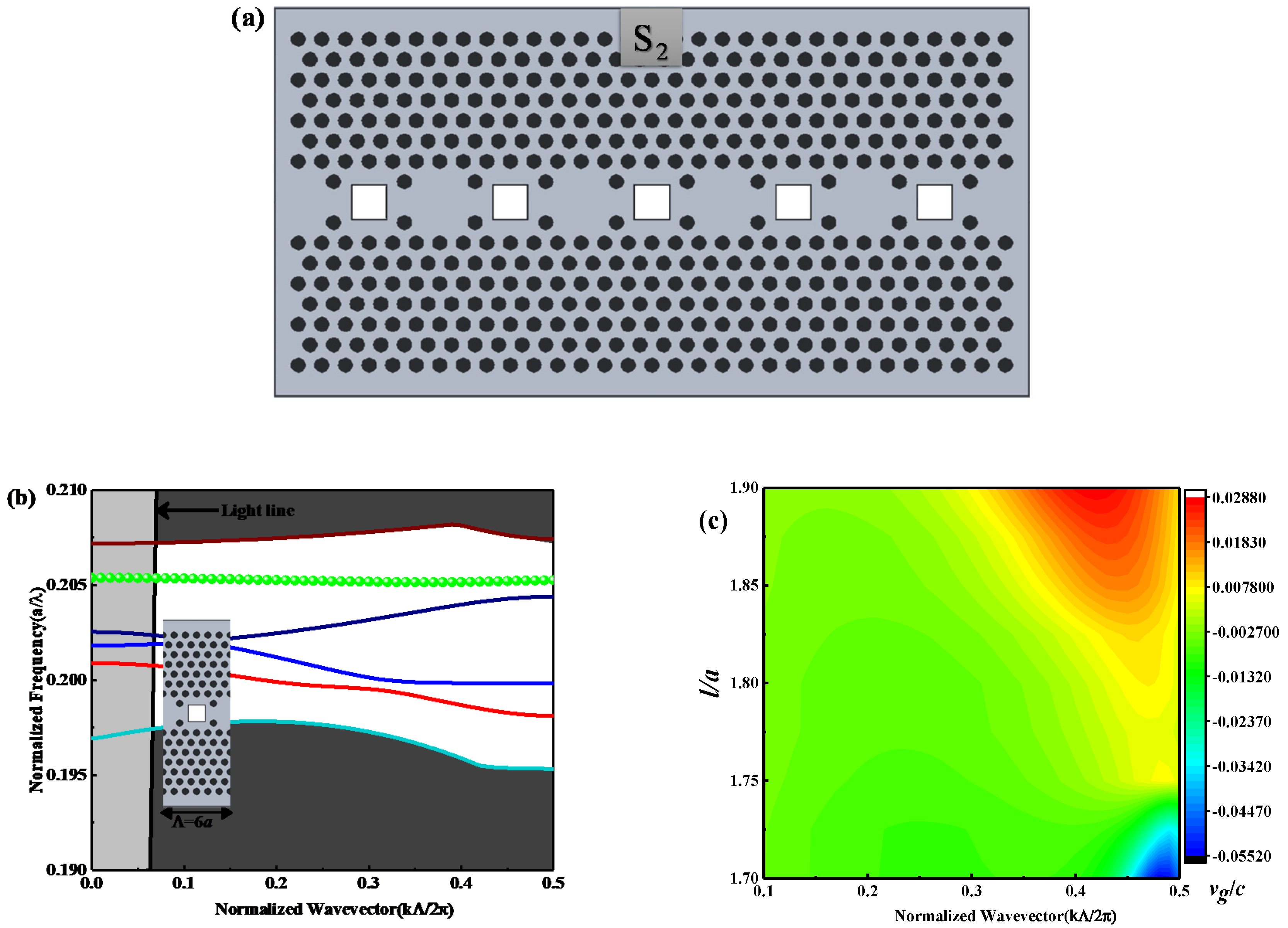
3. Structure Geometry and Simulation Results

The proposed SP-CS-SPCW structure is based on a triangular lattice photonic crystal made from a silicon substrate with refractive index n s i = 3.48 and basic holes filled with highly nonlinear poled electro-optic polystyrene of n p o l y = 1.59 , with elementary radius R = 0.30 a . The coupled-slot cavity waveguide S1 is first constituted by inserting square air slots of length l into the center of the waveguide, as shown in Figure 1a. Afterward, the square air slots will be filled by the ionic liquid. The spacing between each two neighboring square slots is 3 a . Suppose, for example, that the dielectric constant is independent on the Y-axis. At that point, the solutions of all take the form of either transverse magnetic (TM) modes with nonzero ( H y ,   E x ,   E z ) (H field refer to Magnetic component and E field refer to Electric component.) or transverse electric (TE) modes with nonzero ( H x ,   H z ,   E y ) . Our proposed structures support TM only. Figure 1b displays the dispersion curve for TM mode of the square slot defect at l = 1.30 a of S1, i.e., the first derivative between the normalized frequency U = ω a / 2 π c = a / λ and the normalized wavevector K = k a / 2 π for the dispersion relation of the guided mode. The slope of the dispersion curve gives n g that is acquired from Equation (1) by the first derivative of the dispersion curve. Accordingly, from n g Equation and dispersion curve, as shown in Figure 1b, when U is almost unchanged it refers to a flat area of guided mode with changing K, n g going to ultra-high value or infinity, then going to slow-light flat band with a constant slope, which refers to constant n g during changing U with K. S1 SP-CS-SPCW maintained multi-modes inside the Photonic Band Gap (PBG). In this study, we were concerned with the green-guided mode, due to its wide transmission bandwidth. The dispersion curves in Figure 1b were obtained by the plane-wave expansion method (PWE) with the BandSOLVE module of software Rsoft and the inset of Figure 1b is the supercell selected for eigenmode calculations. The solid black line indicates the light line. Figure 1c shows the group velocity v g / c contour map with l varying from 1.20 a to 1.55 a via normalized wavevector K = k Λ / 2 π . We can see that the linearity at the long K range decreases with increasing l until l = 1.40 a but with high group velocity value, namely low group index.
For the comprehension of slow-light devices, the dispersion curves of guided modes should be below the light line, as the guided modes above the light line are lossy and those under the light line are intrinsically lossless [25]. For near-zero group velocity, a high group index S2 SP-CS-SPCW is presented by removing one square slot and remains the other, to form the coupling between slab and slot for increasing the quality factor of each slot cavity and, thus, the filed localization inside the cavity, as shown in Figure 2a. Hence, the spacing between each two neighboring square slot cavities is 6 a . Accordingly, the width of the supercell, as shown by the inset of Figure 2b, becomes 6 a . Figure 2b displays the dispersion curve for TM mode. Figure 2c shows the square slot defect of l = 1.80 a with a flat band for the normalized group velocity ( v g / c ) with l varying from 1.70 a to 1.90 a . Besides, for additionally indistinct observation for the transmission bandwidth and group index variations, Figure 3a,b shows the variation of n g with normalized frequency for TM modes as l changing from 1.225 a   to   1.35 a and 1.70 a   to   1.90 a , respectively, with an increment of l = 0.025 a . It is obvious from Figure 3 that the performance of the guided modes of slow light is significantly affected by the geometrical length of the square slot. The guided modes of the slow light shift in the two structures, S1 and S2, to the higher frequency area as the slot length increases. This is physically understandable. As the length increases, the effective refractive index of the structure decreases, so that the optical size of the structure decreases and, thus, the frequency response scales to the high-frequency area.
From Figure 3a, we can obtain a wider bandwidth with a closely constant dispersion curve slope, i.e., flat band of zero-dispersion area for large NDBP and high-capability optical buffering but with low n g . On the other hand, higher n g can be obtained from Figure 3a with narrower transmission bandwidth. To analyze the data results theoretically, we transferred the results in Figure 3 into Table 1. Based on the PWE method, which deals with infinite structure area, a longer delay-line length L is taken as 1 mm by cascading the unit cell structure shown in Figure 1b and Figure 2b, which is much longer than the wavelength. So, our calculations are applicable [17]. The operating bandwidth was calculated for within ±10% variation of n g as the operating wavelength changes. The lattice constant a is changed to acquire a center wavelength of 1550 nm. It should be noted that, with the scaling characteristic of PhCs, the relationship between the operational wavelength λ and the lattice constant a can be expressed as [26] a = U 0 λ 0 , where U 0 is the central normalized measured frequency for each given n g . Therefore, the properties of PhC can remain unchanged, provided one expands or decreases the parameters of the PCW structure proportionally. One can select the value of the optimum operating wavelength of the structure by only setting the value of a without repeating the simulation [25]. In practical application, the PhC device can be designed according to the demand of the delay time and storage capacity. For better showing the improvement of slow-light property, the corresponding buffering parameters are also shown in Table 1. It can be seen from Figure 3 and Table 1 that, for S1 at l = 1.225 a, the highest bandwidth with a zero-dispersion flat band was obtained at about ∆λ = 104.81 nm, however, with the lowest average group index of n ¯ g   = 9.5, and the storage time was the lowest at about T s = 31.667ps. According to Equation (4), it corresponds to a high bit rate in the range of terabit about R b = 3.2718   Tb / s , which is suitable for signal transmission application, whereas it is preferable for signal buffering at l = 1.25 a , which corresponds to the highest FoM, i.e., NDBP = 0.66313, which is the highest compatible value between n ¯ g and U . A high storage capacity C of 213.912 bit along 1-mm delay-line length is obtained with the delay time in picosecond range. This case maybe become useful for the future 6G mobile communication network due to its highest R b with the smallest L b i t at around 4.6748   μ m . Meanwhile, for S2 at l = 1.725a, the highest bandwidth with zero-dispersion flat band was obtained at about ∆λ = 2.9488 nm, however with a high average group index of n ¯ g = 144 that leads to longer delaying time of 480 ps. By increasing l , the ultra-low group velocity can be acquired (high group index) with accomplishment delaying time of ns range (1.603 ns). Nevertheless, to store 1 bit, a long bit length of 11.3158   μ m is obtained. Such an increase of bit length is due to the decrease of cavity density along the horizontal axis of waveguide, because each cavity serves a center of the stored data. Consequently, the proposed S2 SP-CS-SPCW is suitable for optical switching and high-speed optical modulator at this value of l .
Therefore, we can consider S2 SP-CS-SPCW for the longest storage time and S1 SP-CS-SPCW for wider bandwidth and high transmission bit rate. Figure 4 shows the magnetic field (M-field) profile of pulse transmission inside the optimum structures for S1 at l = 1.25 a and S2 at l = 1.725 a . In Figure 4a, the field distribution spreads out the waveguide with strong coupling between successive slots. Additionally, periodic oscillations for the field contour are detected along the propagation path. In contrast, in Figure 4b, the localization is increased inside the slab with a longer time for making a hop from one cavity to another, which reflects the lower transmission bandwidth with the ultra-low group velocity. The packet compression and decompression may prove useful in high-speed communication and signal processing, including multiplexers. For further optimization and showing the effect of RTIL infiltrated, the square slots are assumed to be filled by ionic liquid whose reflective index is from 1.6 to 1.7 for optical communication wavelength [11]. The main factor for the theoretical calculations is the refractive index. So, we have done our calculations for low and high indices of RTILs’ ranges to meet wide applications. However, there are limited choices for chemically and physically stable, nontoxic liquids as optical materials, especially when the required refractive index is higher than 1.60. Commercially available high-index liquids are often based on harmful or toxic materials, such as liquids based on diiodomethane [27]. High-index RTILs were verified to be appropriate candidates, in this case, to be useful as index-matching liquids [27,28]. Some ILs, especially the early ones, are not stable and these ILs are to be avoided for applications. Many of the new-generation ILs are stable and can be used in the proposed structures. Figure 5 and Table 2 show the slow-light properties, n g and GVD, of the optimum S1 SP-CS-SPCW at l = 1.25 a with the refractive index of RTIL ( n f ) varying from   1.3   to   2.1 . It can be seen that the performance of the guided slow-light modes is significantly affected also by the refractive index of RTIL infiltrated.
The guided modes of the slow light shift to the lower frequency area and the bandwidth increases when the refractive index of RTIL decreases slightly for n f < 1.8 . The shift of mode frequency is physically understandable as the effective refractive index of the structure increases, so that the optical size of the structure increases and, thus, the frequency response scales to the low-frequency area. Table 2 shows the improvement of slow-light property and buffering parameters for the slot holes infiltrated with RTILs with varying n f from 1.3 to 2.1. Polymerized RTILs enhance the transmission rate through optical materials. From the optical properties of polymerized RTILs, it shows that the optimum FoM at high index polymerized RTILs of n f = 1.8 is 0.72402. For 6G networks, the transmission data rate can be 1–10 Tb/s [29,30]. As shown in Table 2, ultra-wide frequency bandwidth is obtained with a high bit rate of about 3.93629   Tb / s with a high R b of 3.93629   Tb / s , which is so high that they are never seen in the literature, and L b i t is enhanced to be 4.2817 μm. PhCs are made of lossless materials [31,32]. However, in reality, all materials have some loss. So, the loss of PhCs could be a factor to be considered in their applications. Fortunately, due to the small size of optical integrated chips, the material loss can be ignored for available materials and, further, the structure losses can be reduced or eliminated through carefully designing the dispersion of the waveguides, explained in detail at [17,33,34,35]. Therefore, PhCs have great potential for information and communication technologies, including 6G wireless communication [31]. Their potential applications for micro-optical components include waveguides, micro-resonators, and photonic crystals, which are essential components in photonic integrated circuits (PICs).

4. Implementation Considerations
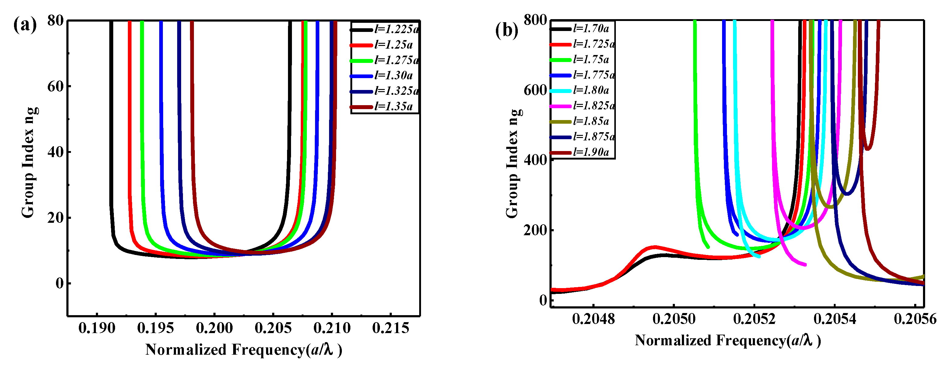
Some restrictions can appear for practical realization of the buffer devices, such as dispersion and losses.

4.1. Dispersion

One of the main factors restricting short-pulse light transmission is material dispersion that induces GVD, which causes pulse width expansion and induces phase modulation. Accordingly, the transmitted light pulse that carries the data bits turns out to be vastly distorted during the propagation path. Thus, the distortion compensation by the GVD is needed in the transmission [36]. For the compensation resolves, the designs with positive and negative GVDs are shown in Figure 5b. Additionally, the slow light transmitted in the waveguide, in general, is intrinsic dispersion. Henceforth, designing a wide zero-dispersion flat band is required. From Figure 5b, it can be observed that GVD is less than 10 6   a / 2 π c 2 in the near-zero-dispersion flat band, which is an adequate GVD because the value of GVD below 10 6   a / 2 π c 2 can be considered as low GVD [37]. Moreover, it is interesting to note that the GVD changes with negative and positive values in the operating frequency range, which is suitable for dispersion compensation applications.

4.2. Losses

Overall, there are two types of losses: Material and structure losses. By choosing the appropriate materials, the material loss can be ignored or avoided [38,39]. The structure loss for the buffer devices or any kind of waveguide comes from two aspects. The first one is the coupling loss at the input and output of structures or devices. The second one is the propagation losses over the buffer device region. To keep the bandwidth and the advantages of buffer devices, it is suitable to employ traditional Si waveguide as a transmission intermediate devoid of any loss and use buffer devices as active elements [35]. Now, the coupling loss can be considered as a frequently resolved issue [35]. Propagation losses in the buffer device region can be divided into intrinsic and extrinsic losses. For the practical realization of the buffer devices, the dispersion curves of waveguide modes would be below the light line, because the modes positioned above the light line are highly loss, and the modes under the light line are intrinsically lossless [25]. All the calculations have been done under light lines in the proposed structures. Professionally, both dispersion and loss issues are controlled by specific designs of the proposed structures, since the advantageous characteristic of slow light is a collaborative result through the broadening of pulse and loss [40].
The proposed SP-CS-SPCW provides an abundantly advanced value of the slow-light property (NDBP) and all optical buffering parameters compared with all other structures, reported previously in the literature, as shown in Table 3. In comparison with other works, we found that our work has high NDBP and the largest transmission bit rate. High-speed communication and signal processing are interoperating fields. To transmit any signal over a wide range (from baseband to bandpass), the modulation technique is used. The analog data in the form of voice, image, or video captured is converted into a digital format, which is further processed for long-range communication. So, processing of digital data requires signal processing, and transmitting this data over long-range requires wireless or fiber communication. Digital signal processing is used because it is more immune to noise and is secured, cheap, and easy to process. Generally, the processed digital data is encoded for sources and channels to give protection and compression simultaneously. The proposed SP-CS-SPCW can find the application in this area, as high-speed optical communication systems require signal processing, e.g., signal modulation and encoding/decoding, while signal processing generally requires data buffering. So, the proposed structure is useful.

5. Conclusions

Slow-light low dispersion and buffering properties in the coupled-slot slot and coupled-slot slab cavities’ waveguide were studied in detail by appropriately modifying the square air slot length. In the proposed SP-CS-SPCW, we obtained a flat band of zero dispersion with the combined constant group index ranging from 8.26 to 481. Moreover, this variation is simultaneous with the changing of delaying time from 30.5 ps to a long delay time of 1603.3 ps. Light propagating by long delaying time and high group index affords the opportunities for advancing photonic integration with permitting compact switches of ultra-small electro-optical devices. Furthermore, the smallest physical length of each storage bit was obtained as L b i t = 4.2817 μm, which is ultra-small. Additionally, in the further optimized case, we infiltrated the slots with RTILs, which boosted the bandwidth to 126.09 nm. From the optical properties of polymerized RTILs, they seem to be promising materials for the fabrication of infrared photonic elements. Their potential applications for micro-optical components include waveguides, micro-resonators, and photonic crystals, which are essential components in photonic integrated circuits (PICs). Finally, the proposed SP-CS-SPCW can find application in this area, as high-speed optical communication systems require signal processing, e.g., signal modulation and encoding/decoding, while signal processing generally requires data buffering. So, the proposed structure is useful. Moreover, it is interesting to note that the GVD changes with negative and positive values in the operating frequency range, which is suitable for dispersion compensation applications.

Author Contributions

Writing—original draft preparation, I.A.; methodology, S.E.; writing—review and editing, Z.O. All authors have read and agreed to the published version of the manuscript.

Funding

This research was funded by the National Natural Science Foundation of China (Grant Nos.: 61275043, 61307048, 60877034, and 61605128), Guangdong Province Natural Science Founds (GDNSF), China (Grant No.: 2020A1515010157), and Shenzhen Science Funds (SZSF), China (Grant No. JCYJ20190808151017218, 20180123).

Conflicts of Interest

The authors declare that they have no known competing financial interests or personal relationships that could have appeared to influence the work reported in this paper.

References

  1. Uddin, M.A.; Chan, H.P. The challenges in the fabrication of reliable polymer photonic devices. J. Mater. Sci. Mater. Electron. 2008, 20, 277–281. [Google Scholar] [CrossRef]
  2. Kruse, K.; Middlebrook, C. Laser-direct writing of single mode and multi-mode polymer step index waveguide structures for optical backplanes and interconnection assemblies. Photon Nanostruct. Fundam. Appl. 2015, 13, 66–73. [Google Scholar] [CrossRef]
  3. Oh, M.-C.; Chu, W.-S.; Shin, J.-S.; Kim, J.-W.; Kim, K.-J.; Seo, J.-K.; Lee, H.-K.; Noh, Y.-O.; Lee, H.-J. Polymeric optical waveguide devices exploiting special properties of polymer materials. Opt. Commun. 2016, 362, 3–12. [Google Scholar] [CrossRef]
  4. Krauss, T.F. Why Do We Need Slow Light? Nat. Photonics 2008, 2, 448–449. [Google Scholar] [CrossRef]
  5. Wu, X.; Muntzeck, M.; Arcos, T.D.L.; Grundmeier, G.; Wilhelm, R.; Wagner, T. Determination of the refractive indices of ionic liquids by ellipsometry, and their application as immersion liquids. Appl. Opt. 2018, 57, 9215–9222. [Google Scholar] [CrossRef]
  6. Higashino, Y.; Isobe, T.; Matsushita, S.; Nakajima, A. Preparation and properties of transparent solid–liquid hybrid materials using porous silica with silicone oil or ionic liquid. Mater. Res. Bull. 2020, 130, 110902. [Google Scholar] [CrossRef]
  7. Park, J.H.; Ko, I.J.; Kim, G.W.; Lee, H.; Jeong, S.H.; Lee, J.Y.; Lampande, R.; Kwon, J.H. High transmittance and deep RGB primary electrochromic color filter for high light out-coupling electro-optical devices. Opt. Express 2019, 27, 25531–25543. [Google Scholar] [CrossRef]
  8. Watanabe, M.; Thomas, M.L.; Zhang, S.; Ueno, K.; Yasuda, T.; Dokko, K. Application of Ionic Liquids to Energy Storage and Conversion Materials and Devices. Chem. Rev. 2017, 117, 7190–7239. [Google Scholar] [CrossRef] [Green Version]
  9. Qiu, M.; Zhang, B.; Wu, H.; Cao, L.; He, X.; Li, Y.; Li, J.; Xu, M.; Jiang, Z. Preparation of anion exchange membrane with enhanced conductivity and alkaline stability by incorporating ionic liquid modified carbon nanotubes. J. Membr. Sci. 2019, 573, 1–10. [Google Scholar] [CrossRef]
  10. Nasirpour, N.; Mohammadpourfard, M.; Heris, S.Z. Ionic liquids: Promising compounds for sustainable chemical processes and applications. Chem. Eng. Res. Des. 2020, 160, 264–300. [Google Scholar] [CrossRef]
  11. Rola, K.P.; Zajac, A.; Czajkowski, M.; Cybinska, J.; Martynkien, T.; Smiglak, M.; Komorowska, K. Ionic liquids—A novel material for planar photonics. Nanotechnology 2018, 29, 475202. [Google Scholar] [CrossRef] [PubMed]
  12. Rola, K.P.; Zajac, A.; Czajkowski, M.; Fiedot-Tobola, M.; Szpecht, A.; Cybinska, J.; Smiglak, M.; Komorowska, K. Electron Beam Patterning of Polymerizable Ionic Liquid Films for Application in Photonics. Langmuir 2019, 35, 11968–11978. [Google Scholar] [CrossRef] [PubMed]
  13. Huang, Y.; Paloczi, G.T.; Yariv, A.; Zhang, C.; Dalton, L. Fabrication and Replication of Polymer Integrated Optical Devices Using Electron-Beam Lithography and Soft Lithography. J. Phys. Chem. B 2004, 108, 8606–8613. [Google Scholar] [CrossRef]
  14. Sun, H.; Chen, A.; Olbricht, B.C.; Davies, J.A.; Sullivan, P.A.; Liao, Y.; Dalton, L. Direct electron beam writing of electro-optic polymer microring resonators. Opt. Express 2008, 16, 6592–6599. [Google Scholar] [CrossRef] [PubMed]
  15. Minamimoto, H.; Irie, H.; Uematsu, T.; Tsuda, T.; Imanishi, A.; Seki, S.; Kuwabata, S. Polymerization of Room-Temperature Ionic Liquid Monomers by Electron Beam Irradiation with the Aim of Fabricating Three-Dimensional Micropolymer/Nanopolymer Structures. Langmuir 2014, 31, 4281–4289. [Google Scholar] [CrossRef] [Green Version]
  16. Frandsen, L.H.; Lavrinenko, A.V.; Fage-Pedersen, J.; Borel, P.I. Photonic crystal waveguides with semi-slow light and tailored dispersion properties. Opt. Express 2006, 14, 9444–9450. [Google Scholar] [CrossRef] [Green Version]
  17. Elshahat, S.; Abood, I.; Khan, K.; Yadav, A.; Bibbo, L.; Ouyang, Z. Five-Line Photonic Crystal Waveguide for Optical Buffering and Data Interconnection of Picosecond Pulse. J. Light. Technol. 2018, 37, 788–798. [Google Scholar] [CrossRef]
  18. Ma, J.; Jiang, C. Demonstration of Ultraslow Modes in Asymmetric Line-Defect Photonic Crystal Waveguides. IEEE Photon Technol. Lett. 2008, 20, 1237–1239. [Google Scholar] [CrossRef]
  19. Baba, T. Slow light in photonic crystals. Nat. Photonics 2008, 2, 465. [Google Scholar] [CrossRef]
  20. Zhai, Y.; Tian, H.; Ji, Y. Slow Light Property Improvement and Optical Buffer Capability in Ring-Shape-Hole Photonic Crystal Waveguide. J. Light. Technol. 2011, 29, 3083–3090. [Google Scholar] [CrossRef]
  21. Zhao, Y.; Zhang, Y.; Wang, Q.; Hu, H. Review on the Optimization Methods of Slow Light in Photonic Crystal Waveguide. IEEE Trans. Nanotechnol. 2015, 14, 407–426. [Google Scholar] [CrossRef]
  22. Zhao, Y.; Zhang, Y.; Hu, H. Dispersion Engineering of Slow Light in Ellipse-Shaped-Hole Slotted Photonic Crystal Waveguide. J. Light. Technol. 2014, 32, 2144–2151. [Google Scholar] [CrossRef]
  23. Elshahat, S.; Abood, I.; Khan, K.; Yadav, A.; Ouyang, Z. High-capability micro-optical buffer based on coupled hexagonal cavity in photonic crystal waveguide. Appl. Nanosci. 2019, 9, 1963–1970. [Google Scholar] [CrossRef]
  24. Tucker, R.; Ku, P.-C.; Chang-Hasnain, C. Slow-light optical buffers: Capabilities and fundamental limitations. J. Light. Technol. 2005, 23, 4046–4066. [Google Scholar] [CrossRef]
  25. Elshahat, S.; Abood, I.; Khan, K.; Yadav, A.; Wang, Q.; Liu, Q.; Lin, M.; Tao, K.; Ouyang, Z. Ultra-wideband slow light transmission with high normalized delay bandwidth product in W3 photonic crystal waveguide. Superlattices Microstruct. 2018, 121, 45–54. [Google Scholar] [CrossRef]
  26. Elshahat, S.; Khan, K.; Yadav, A.; Bibbò, L.; Ouyang, Z. Slow-light transmission with high group index and large normalized delay bandwidth product through successive defect rods on intrinsic photonic crystal waveguide. Opt. Commun. 2018, 418, 73–79. [Google Scholar] [CrossRef]
  27. Deetlefs, M.; Seddon, K.R.; Shara, M. Neoteric optical media for refractive index determination of gems and minerals. New J. Chem. 2006, 30, 317. [Google Scholar] [CrossRef]
  28. Kayama, Y.; Ichikawa, T.; Ohno, H. Transparent and colourless room temperature ionic liquids having high refractive index over 1. Chem. Commun. 2014, 50, 14790–14792. [Google Scholar] [CrossRef]
  29. Alsharif, M.H.; Kelechi, A.H.; Albreem, M.A.M.; Chaudhry, S.A.; Zia, M.S.; Kim, S. Sixth Generation (6G) Wireless Networks: Vision, Research Activities, Challenges and Potential Solutions. Symmetry 2020, 12, 676. [Google Scholar] [CrossRef]
  30. You, X.H.; Wang, C.-X.; Huang, J.; Gao, X.Q.; Zhang, Z.; Wang, M.; Huang, Y.; Zhang, C.; Jiang, Y.X.; Jiaheng, W.; et al. Towards 6G wireless communication networks: Vision, enabling technologies, and new paradigm shifts. Sci. China Inf. Sci. 2020, 1–83. [Google Scholar] [CrossRef]
  31. Yang, Y.; Yamagami, Y.; Yu, X.; Pitchappa, P.; Webber, J.; Zhang, B.; Fujita, M.; Nagatsuma, T.; Singh, R. Terahertz topological photonics for on-chip communication. Nat. Photonics 2020, 14, 446–451. [Google Scholar] [CrossRef] [Green Version]
  32. Tsuruda, K.; Fujita, M.; Nagatsuma, T. Extremely low-loss terahertz waveguide based on silicon photonic-crystal slab. Opt. Express 2015, 23, 31977–31990. [Google Scholar] [CrossRef] [PubMed]
  33. O’Faolain, L.; Schulz, S.A.; Beggs, D.M.; White, T.E.; Spasenović, M.; Kuipers, L.; Morichetti, F.; Melloni, A.; Mazoyer, S.; Hugonin, J.-P.; et al. Loss engineered slow light waveguides. Opt. Express 2010, 18, 27627–27638. [Google Scholar] [CrossRef] [PubMed] [Green Version]
  34. Schulz, S.A.; O’Faolain, L.; Beggs, D.M.; White, T.E.; Melloni, A.; Krauss, T.F. Dispersion engineered slow light in photonic crystals: A comparison. J. Opt. 2010, 12, 104004. [Google Scholar] [CrossRef]
  35. Dutta, H.S.; Goyal, A.K.; Srivastava, V.; Pal, S. Coupling light in photonic crystal waveguides: A review. Photon Nanostruct. Fundam. Appl. 2016, 20, 41–58. [Google Scholar] [CrossRef]
  36. Krauss, T.F. Slow light in photonic crystal waveguides. J. Phys. D Appl. Phys. 2007, 40, 2666–2670. [Google Scholar] [CrossRef] [Green Version]
  37. Elshahat, S.; Abood, I.; Liang, Z.; Pei, J.; Ouyang, Z. Futuristic elongated-hexagonal photonic crystal waveguide for slow light. Opt. Commun. 2020, 474, 126082. [Google Scholar] [CrossRef]
  38. Palik, E. (Ed.) This page is intentionally left blank. In Handbook of Optical Constants of Solids; Elsevier BV: Amsterdam, The Netherlands, 1997; 1000p. [Google Scholar]
  39. Yan, S.; Cheng, Z.; Frandsen, L.H.; Ding, Y.; Zhou, F.; Dong, J.; Zhang, X. Bandwidth-adaptable silicon photonic differentiator employing a slow light effect. Opt. Lett. 2017, 42, 1596–1599. [Google Scholar] [CrossRef]
  40. Vlasov, Y.A.; O’Boyle, M.; Hamann, H.F.; McNab, S.J. Active control of slow light on a chip with photonic crystal waveguides. Nature 2005, 438, 65–69. [Google Scholar] [CrossRef]
  41. Serna, S.; Colman, P.; Zhang, W.; Le Roux, X.; Caer, C.; Vivien, L.; Cassan, É. Experimental GVD engineering in slow light slot photonic crystal waveguides. Sci. Rep. 2016, 6, 26956. [Google Scholar] [CrossRef] [Green Version]
  42. Elshahat, S.; Abood, I.; Liang, Z.; Pei, J.; Ouyang, Z. Sporadic-Slot Photonic-Crystal Waveguide for All-Optical Buffers With Low-Dispersion, Distortion, and Insertion Loss. IEEE Access 2020, 8, 77689–77700. [Google Scholar] [CrossRef]
  43. Aghababaeian, H.; Vadjed-Samiei, M.-H.; Granpayeh, N. Temperature Stabilization of Group Index in Silicon Slotted Photonic Crystal Waveguides. J. Opt. Soc. Korea 2011, 15, 398–402. [Google Scholar] [CrossRef] [Green Version]
Figure 1. (a) Schematic structure of the proposed S 1   S P C S S P C W geometry based on triangular-lattice photonic crystal made up of holes filled with electro-optic polystyrene (refractive index n p o l y = 1.59 ) with basic hole radius R = 0.30 a in a silicon substrate of n s i = 3.48 ; (b) the dispersion curve for T M   w i t h   l = 1.30 a , where the inset shows the supercell used for simulation; (c) the normalized-group velocity ( v g / c ) contour map with l varying from 1.20 a to 1.55 a via normalized wavevector K .
Nanomaterials 10 01742 g001
Figure 2. (a) Schematic structure of the proposed S2 SP-CS-SPCW geometry; (b) the dispersion curve for TM with l = 1.80 a , where the inset shows the supercell used for simulation; (c) the normalized group velocity ( v g / c ) contour map with l varying from 1.70 a to 1.90 a via normalized wavevector K .
Nanomaterials 10 01742 g002
Figure 3. The group index ( n g ) versus normalized frequency a / λ with changing defect length l for (a) S1 and (b) S2.
Nanomaterials 10 01742 g003
Figure 4. The magnetic field profile of pulse transmission inside the optimum structures for (a) S1 at l = 1.25 a and (b) S2 at l = 1.725 a .
Nanomaterials 10 01742 g004
Figure 5. Slow-light properties of the optimum S1 SP-CS-SPCW for refractive indices of R T I L s ( n ) varying from 1.3 to 2.1 at l = 1.25 a versus normalized frequency a / λ for (a) group index ( n g ) and (b) group-velocity dispersion ( G V D ) .
Nanomaterials 10 01742 g005
Table 1. Slow-light parameters and buffering capability under different values of l for S1 and S2.
Structure l / a n ¯ g U λ   ( nm ) NDBP T s   ( ps ) C ( b i t ) L b i t ( μ m ) R b ( T b / s )
S11.2259.50.01343104.810.6423731.667207.2154.82593.2718
1.25100.01327102.780.6631333.333213.9124.67483.2087
1.27510.40.0123995.6890.6420534.667207.1124.82832.9872
1.310.720.0116789.4990.6189935.733199.6735.00822.7939
1.325110.0113986.7610.6157336.667198.6215.03472.7085
1.3511.680.010881.9270.6173638.933199.1495.02142.5576
S21.71370.000372.81960.24922456.6780.39312.43898.8 × 10−5
1.7251440.000392.94880.2739548088.37211.31589.2 × 10−5
1.751730.000241.78420.19914576.6764.23815.56715.6 × 10−5
1.7751980.000191.42810.1824366058.84716.99314.5 × 10−5
1.82040.000181.39550.1836768059.24716.87854.4 × 10−5
1.8252420.000131.01530.15852806.6751.13619.55593.2 × 10−5
1.853138.4 × 10−50.63540.128311043.341.39124.162 × 10−5
1.8753486.4 × 10−50.48360.10858116035.02628.551.5 × 10−5
1.94813.5 × 10−50.2670.082861603.326.7337.41078.3 × 10−6
Table 2. Slow-light parameters and buffering capability at different refractive indices of RTILs ( n f from 1.3 to 2.1).
Structure n f n ¯ g U λ   ( nm ) NDBP T s   ( ps ) C ( b i t ) L b i t ( μ m ) R b ( T b / s )
S11.39.330.01387108.130.6508630.5209.9564.76293.37549
1.49.150.01417110.740.6537529.9210.8884.74193.45718
1.58.970.01447113.360.6560229.067211.6194.72553.53878
1.68.720.01481116.470.6552329.433211.3664.73113.63588
1.78.830.01556122.660.6987829.667225.4144.43633.82923
1.88.90.01595126.090.7240228.8233.5534.28173.93629
1.98.640.01521120.150.6697428.233216.0464.62873.75079
2.08.470.01471116.270.6353727.533204.9594.8793.62974
2.18.260.01425112.640.6002830.5193.6375.16433.51642
Table 3. Comparison between current work and previous literature.
Refs.NDBP R b ( T b / s ) C ( b i t ) L b i t ( μ m )
Current work0.724023.93629233.5534.2817
[22]0.14NonNonNon
[41]0.221NonNonNon
[42]0.68582.3125221.24.5202
[43]0.31NonNonNon
[20]0.4661Non143.36.95
[37]0.6456Non NonNon

