Graphene Plasmon Resonances for Electrically-Tunable Sub-Femtometer Dimensional Resolution


 , and
, and 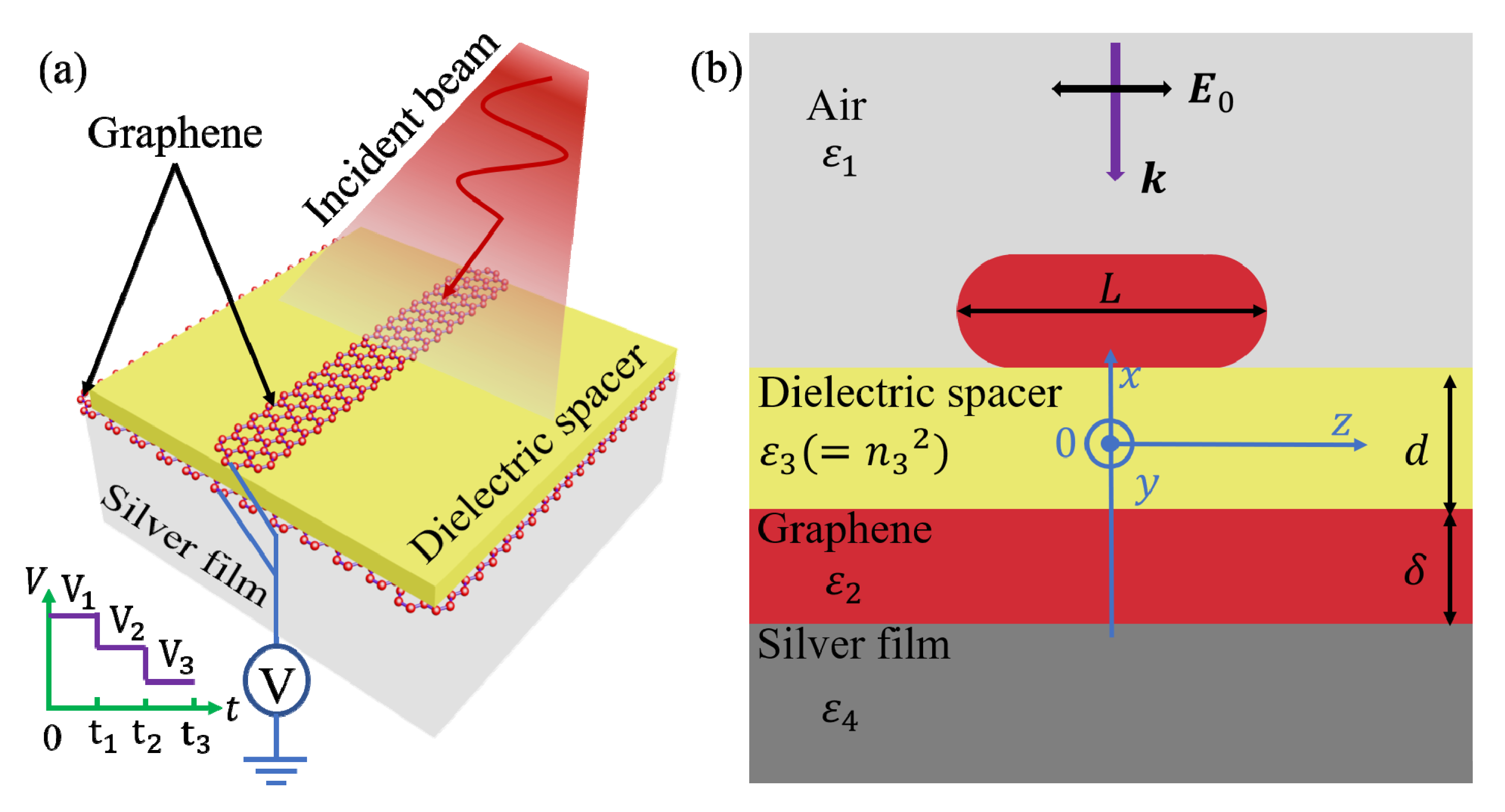
Abstract
1. Introduction
2. Theoretical Model and Method
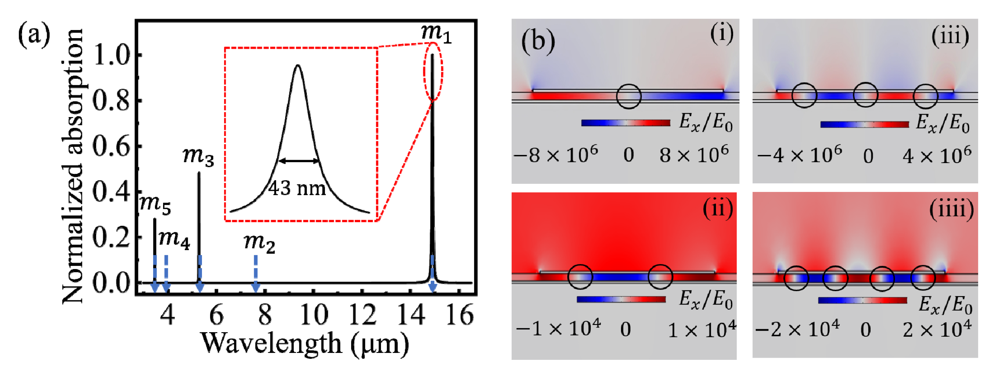
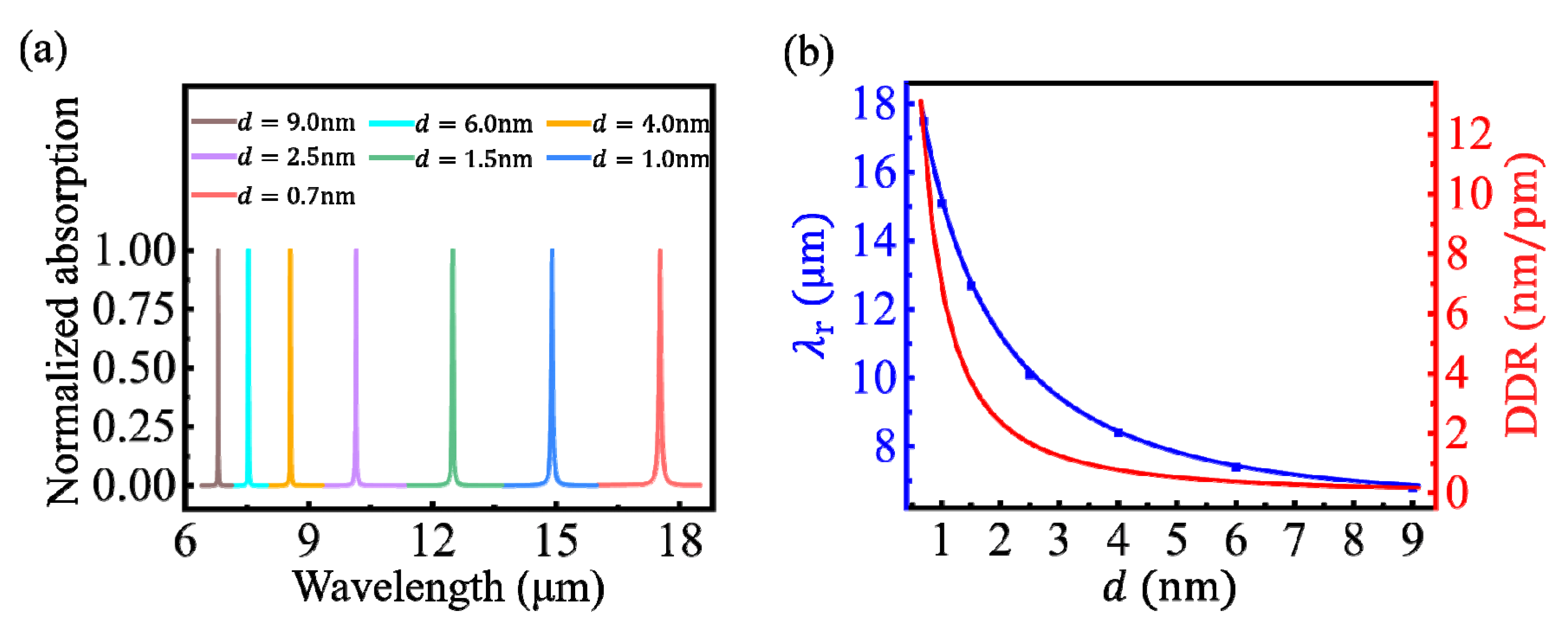
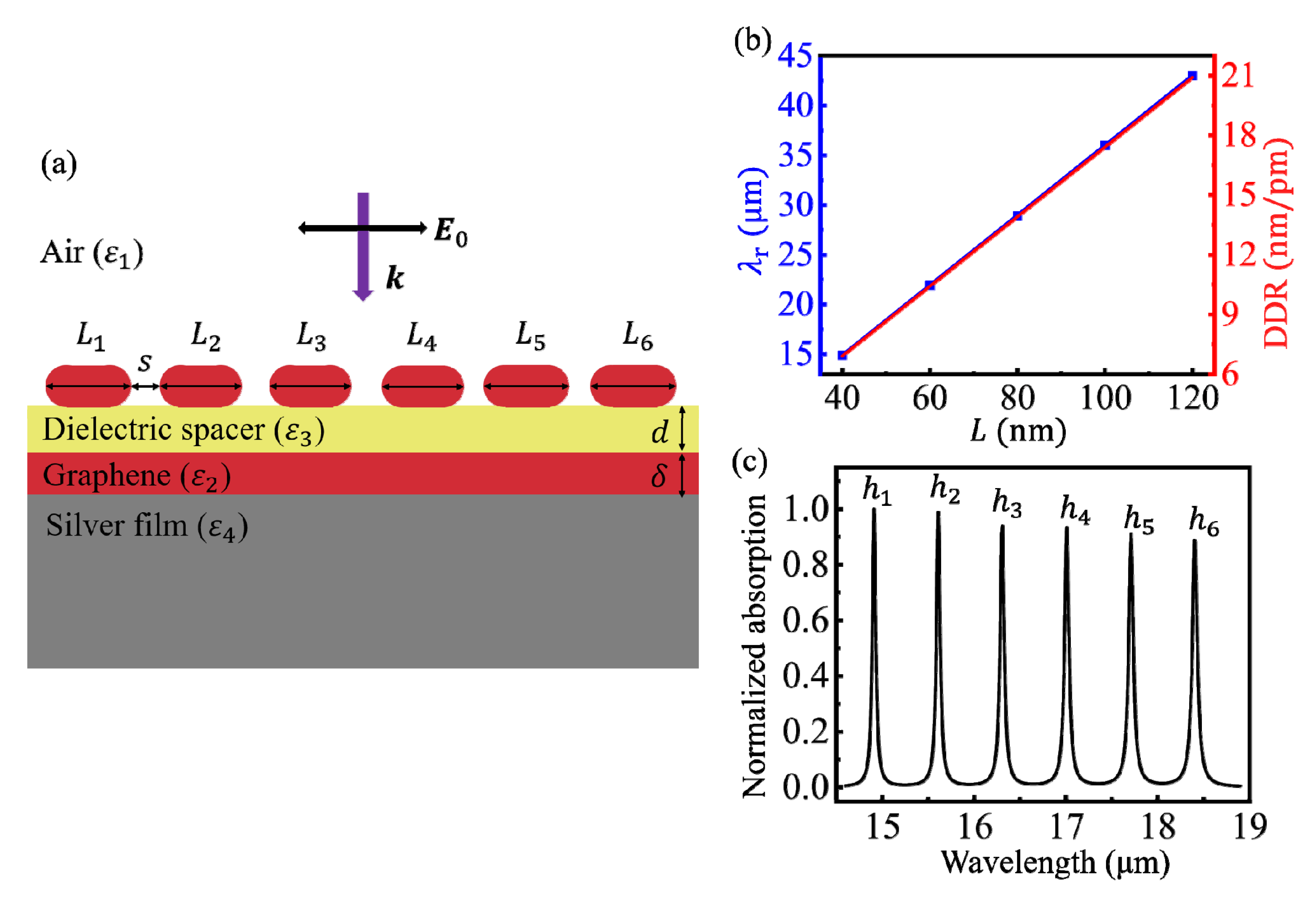
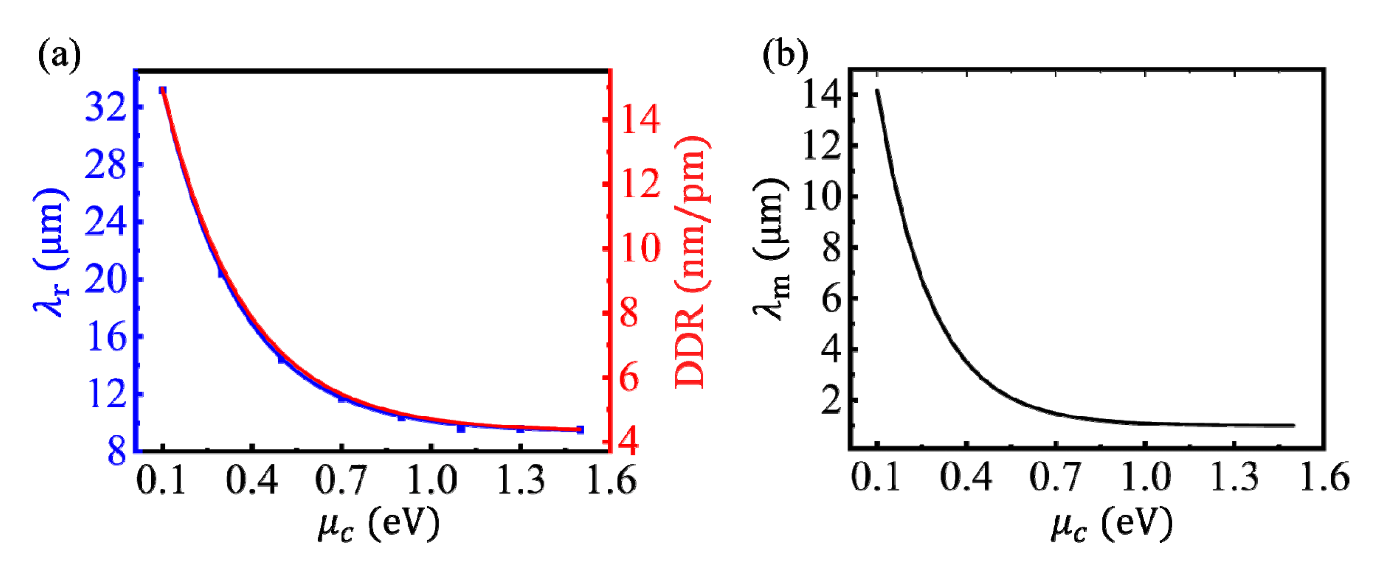
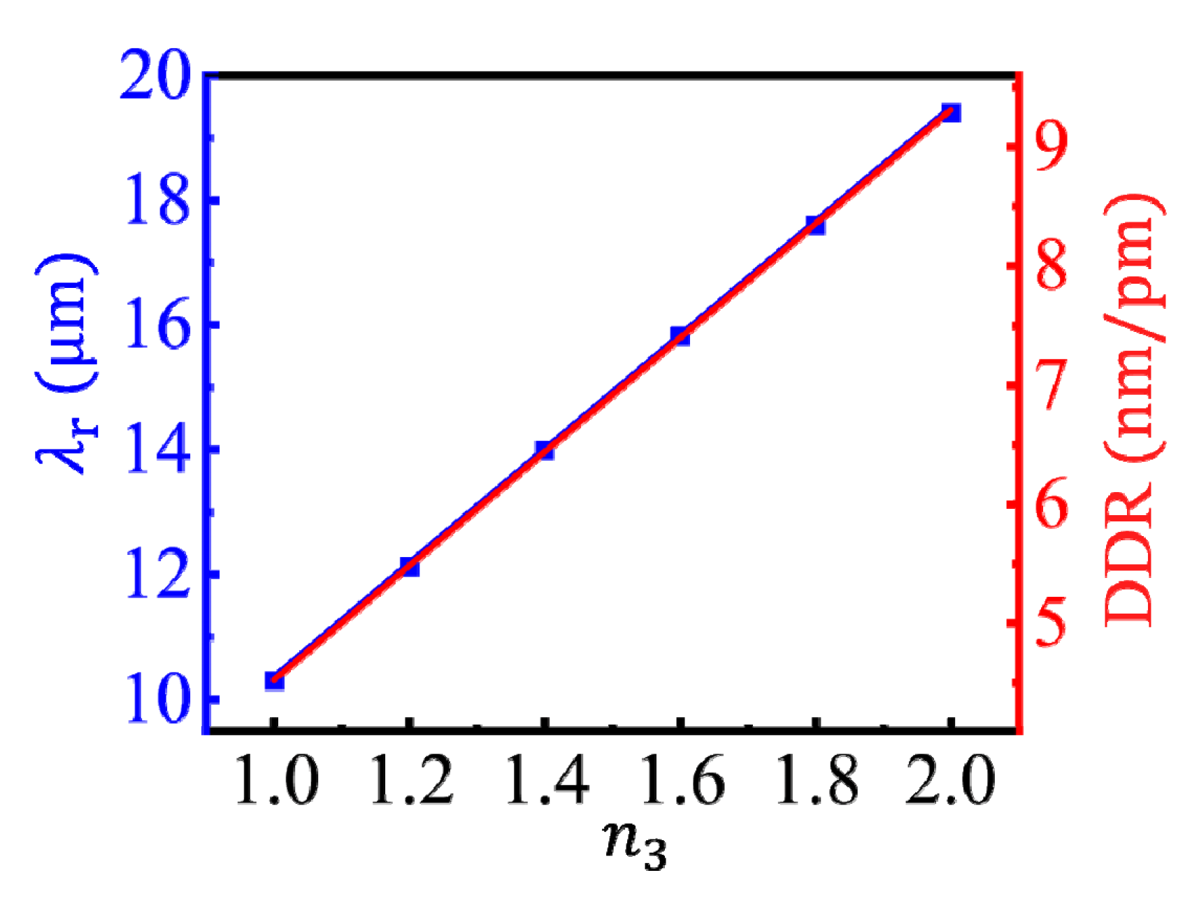
3. Results and Discussion
4. Conclusions
Author Contributions
Funding
Acknowledgments
Conflicts of Interest
References
- Sönnichsen, C.; Reinhard, B.M.; Liphardt, J.; Alivisatos, A.P. A molecular ruler based on plasmon coupling of single gold and silver nanoparticles. Nat. Biotechnol. 2005, 23, 741–745. [Google Scholar] [CrossRef]
- Chen, J.I.L.; Chen, Y.; Ginger, D.S. Plasmonic nanoparticle dimers for optical sensing of DNA in complex media. J. Am. Chem. Soc. 2010, 132, 9600–9601. [Google Scholar] [CrossRef] [PubMed]
- Reinhard, B.M.; Sheikholeslami, S.; Mastroianni, A.; Alivisatos, A.P.; Liphardt, J. Use of plasmon coupling to reveal the dynamics of DNA bending and cleavage by single EcoRV restriction enzymes. Proc. Natl. Acad. Sci. USA 2007, 104, 2667. [Google Scholar] [CrossRef] [PubMed]
- Wang, H.; Reinhard, B.M. Monitoring Simultaneous Distance and Orientation Changes in Discrete Dimers of DNA Linked Gold Nanoparticles. J. Phys. Chem. C 2009, 113, 11215–11222. [Google Scholar] [CrossRef][Green Version]
- Tian, M.; Huang, Y.; Wang, W.; Li, R.; Liu, P.; Liu, C.; Zhang, Y. Temperature-dependent electrical properties of graphene nanoplatelets film dropped on flexible substrates. J. Mater. Res. 2014, 29, 1288–1294. [Google Scholar] [CrossRef]
- Zhao, X.; Long, Y.; Yang, T.; Li, J.; Zhu, H. Simultaneous high sensitivity sensing of temperature and humidity with Graphene Woven Fabrics. ACS Appl. Mater. Interfaces 2017, 9, 30171–30176. [Google Scholar] [CrossRef] [PubMed]
- Wie, J.J.; Wang, D.H.; Lee, K.M.; Tan, L.-S.; White, T.J. Molecular engineering of Azobenzene-Functionalized Polyimides to enhance both photomechanical work and motion. Chem. Mater. 2014, 26, 5223–5230. [Google Scholar] [CrossRef]
- Wang, H.; Song, S.; Zou, X.; Wang, F.; Zhang, Z.; Morozov, S.I.; Wang, X.; Reddy, K.M.; An, Q. Photomechanical effect leading to extraordinary ductility in covalent semiconductors. Phys. Rev. B 2019, 100, 094110. [Google Scholar] [CrossRef]
- Su, K.-H.; Wei, Q.-H.; Zhang, X.; Mock, J.; Smith, D.R.; Schultz, S. Interparticle coupling effects on plasmon resonances of nanogold particles. Nano Lett. 2003, 3, 1087–1090. [Google Scholar] [CrossRef]
- Gunnarsson, L.; Rindzevicius, T.; Prikulis, J.; Kasemo, B.; Käll, M.; Zou, S.; Schatz, G.C. Confined plasmons in nanofabricated single silver particle pairs: Experimental observations of strong interparticle interactions. J. Phys. Chem. B 2005, 109, 1079–1087. [Google Scholar] [CrossRef]
- Hill, R.T.; Mock, J.J.; Hucknall, A.; Wolter, S.D.; Jokerst, N.M.; Smith, D.R.; Chilkoti, A. Plasmon ruler with angstrom length resolution. ACS Nano 2012, 6, 9237–9246. [Google Scholar] [CrossRef] [PubMed]
- Mubeen, S.; Zhang, S.; Kim, N.; Lee, S.; Krämer, S.; Xu, H.; Moskovits, M. Plasmonic properties of gold nanoparticles separated from a gold mirror by an ultrathin oxide. Nano Lett. 2012, 12, 2088–2094. [Google Scholar] [CrossRef] [PubMed]
- Kelly, K.L.; Coronado, E.; Zhao, L.L.; Schatz, G.C. The optical properties of metal nanoparticles: The influence of size, shape, and dielectric environment. J. Phys. Chem. B 2003, 107, 668–677. [Google Scholar] [CrossRef]
- Sönnichsen, C.; Franzl, T.; Wilk, T.; von Plessen, G.; Feldmann, J.; Wilson, O.; Mulvaney, P. Drastic reduction of plasmon damping in gold nanorods. Phys. Rev. Lett. 2002, 88, 077402. [Google Scholar] [CrossRef] [PubMed]
- Jain, P.K.; Lee, K.S.; El-Sayed, I.H.; El-Sayed, M.A. Calculated absorption and scattering properties of gold nanoparticles of different size, shape, and composition: Applications in biological imaging and biomedicine. J. Phys. Chem. B 2006, 110, 7238–7248. [Google Scholar] [CrossRef]
- Jain, P.K.; Huang, W.; El-Sayed, M.A. On the universal scaling behavior of the distance decay of plasmon coupling in metal nanoparticle pairs: A plasmon ruler equation. Nano Lett. 2007, 7, 2080–2088. [Google Scholar] [CrossRef]
- Zhang, J.; Zhang, L. Nanostructures for surface plasmons. Adv. Opt. Photonics 2012, 4, 157–321. [Google Scholar] [CrossRef]
- Esteban, R.N.; Aguirregabiria, G.; Borisov, A.G.; Wang, Y.M.; Nordlander, P.; Bryant, G.W.; Aizpurua, J. The morphology of narrow gaps modifies the plasmonic response. ACS Photonics 2015, 2, 295–305. [Google Scholar] [CrossRef]
- Powell, A.W.; Coles, D.M.; Taylor, R.A.; Watt, A.A.; Assender, H.E.; Smith, J.M. Plasmonic gas sensing using nanocube patch antennas. Adv. Opt. Mater. 2016, 4, 634–642. [Google Scholar] [CrossRef]
- Zhang, F.-L.; Yi, J.; Peng, W.; Radjenovic, P.M.; Zhang, H.; Tian, Z.-Q.; Li, J.-F. Elucidating molecule–plasmon interactions in nanocavities with 2 nm spatial resolution and at the single-molecule level. Angew. Chem. Int. Ed. 2019, 58, 12133–12137. [Google Scholar] [CrossRef] [PubMed]
- Zhang, S.; Xu, H. Tunable dark plasmons in a metallic nanocube dimer: Toward ultimate sensitivity nanoplasmonic sensors. Nanoscale 2016, 8, 13722–13729. [Google Scholar] [CrossRef] [PubMed]
- Hu, H.; Zhang, S.; Xu, H. Closely packed metallic nanocuboid dimer allowing plasmomechanical strong coupling. Phys. Rev. A 2019, 99, 033815. [Google Scholar] [CrossRef]
- Yang, D.-J.; Zhang, S.; Im, S.-J.; Wang, Q.-Q.; Xu, H.; Gao, S. Analytical analysis of spectral sensitivity of plasmon resonances in a nanocavity. Nanoscale 2019, 11, 10977–10983. [Google Scholar] [CrossRef] [PubMed]
- Chen, W.; Zhang, S.; Deng, Q.; Xu, H. Probing of sub-picometer vertical differential resolutions using cavity plasmons. Nat. Commun. 2018, 9, 801. [Google Scholar] [CrossRef]
- Chen, J.; Badioli, M.; Alonso-González, P.; Thongrattanasiri, S.; Huth, F.; Osmond, J.; Spasenović, M.; Centeno, A.; Pesquera, A.; Godignon, P.; et al. Optical nano-imaging of gate-tunable graphene plasmons. Nature 2012, 487, 77–81. [Google Scholar] [CrossRef]
- Amanatiadis, S.; Kantartzis, N. Distortion of surface plasmon polariton propagation on graphene due to chemical potential variation. Appl. Phys. A 2016, 122, 313. [Google Scholar] [CrossRef]
- Bouzianas, G.D.; Kantartzis, N.; Tsiboukis, T.D. Plasmon mode excitation on graphene layers via obliquely-incident focused wideband pulses in rigorous time-domain algorithms. IEEE Trans. Magn. 2013, 49, 1773–1776. [Google Scholar] [CrossRef]
- Liang, H.; Zhang, L.; Zhang, S.; Cao, T.; Alu, A.; Ruan, S.; Qiu, C.-W. Gate-programmable electro-optical addressing array of graphene-coated nanowires with sub-10 nm resolution. Acs Photonics 2016, 3, 1847–1853. [Google Scholar] [CrossRef]
- Mock, A. Padé approximant spectral fit for FDTD simulation of graphene in the near infrared. Opt. Mater. Express 2012, 2, 771–781. [Google Scholar] [CrossRef]
- Vakil, A.; Engheta, N. Transformation optics using graphene. Science 2011, 332, 1291–1294. [Google Scholar] [CrossRef]
- Ma, Q.; Dai, J.; Luo, A.; Hong, W. Numerical and theoretical study of Tunable Plasmonically induced transparency effect based on bright–dark mode coupling in Graphene Metasurface. Nanomaterials 2020, 10, 232. [Google Scholar] [CrossRef] [PubMed]
- Wang, Y.; Liu, H.; Wang, S.; Cai, M.; Zhang, H.; Qiao, Y. Electrical Phase Control Based on Graphene Surface Plasmon Polaritons in Mid-infrared. Nanomaterials 2020, 10, 576. [Google Scholar] [CrossRef] [PubMed]
- Ordal, M.A.; Bell, R.J.; Alexander, R.W.; Long, L.L.; Querry, M.R. Optical properties of fourteen metals in the infrared and far infrared: Al, Co, Cu, Au, Fe, Pb, Mo, Ni, Pd, Pt, Ag, Ti, V, and W. Appl. Opt. 1985, 24, 4493–4499. [Google Scholar] [CrossRef] [PubMed]
- Wu, Z.; Ning, T.; Li, J.; Zhang, M.; Su, H.; Li, I.L.; Liang, H. Tunable photonic-like modes in graphene-coated nanowires. Opt. Express 2019, 27, 35238–35244. [Google Scholar] [CrossRef] [PubMed]
- Huang, Y.; Zhang, L.; Yin, H.; Zhang, M.; Su, H.; Li, I.L.; Liang, H. Graphene-coated nanowires with a drop-shaped cross section for 10 nm confinement and 1 mm propagation. Opt. Lett. 2017, 42, 2078–2081. [Google Scholar] [CrossRef]
- Hanson, G.W. Dyadic Green’s functions and guided surface waves for a surface conductivity model of graphene. J. Appl. Phys. 2008, 103, 064302. [Google Scholar] [CrossRef]
- Jablan, M.; Buljan, H.; Soljačić, M. Plasmonics in graphene at infrared frequencies. Phys. Rev. B 2009, 80, 245435. [Google Scholar] [CrossRef]
- Liang, H.W.; Ruan, S.C.; Zhang, M.; Su, H.; Li, I.L. Characteristics of modified surface plasmon polaritons on double-coated metal nanofilms. Laser Phys. Lett. 2014, 11, 115003. [Google Scholar] [CrossRef]
- Ebbesen, T.W.; Lezec, H.J.; Ghaemi, H.F.; Thio, T.; Wolff, P.A. Extraordinary optical transmission through sub-wavelength hole arrays. Nature 1998, 391, 667–669. [Google Scholar] [CrossRef]
- Gordon, R. Light in a subwavelength slit in a metal: Propagation and reflection. Phys. Rev. B 2006, 73, 153405. [Google Scholar] [CrossRef]
- Chandran, A.; Barnard, E.S.; White, J.S.; Brongersma, M.L. Metal-dielectric-metal surface plasmon-polariton resonators. Phys. Rev. B 2012, 85, 085416. [Google Scholar] [CrossRef]
- Bludov, Y.V.; Ferreira, A.; Peres, N.M.; Vasilevskiy, M.I. A primer on surface plasmon-polaritons in graphene. Int. J. Mod. Phys. B 2013, 27, 1341001. [Google Scholar] [CrossRef]
- Strait, J.H.; Nene, P.; Chan, W.-M.; Manolatou, C.; Tiwari, S.; Rana, F.; Kevek, J.W.; McEuen, P.L. Confined plasmons in graphene microstructures: Experiments and theory. Phys. Rev. B 2013, 87, 241410. [Google Scholar] [CrossRef]
- Gonçalves, P.A.D.; Peres, N.M.R. An Introduction to Graphene Plasmonics; World Scientific: Singapore, 2016. [Google Scholar]
- Vasić, B.; Isić, G.; Gajić, R. Localized surface plasmon resonances in graphene ribbon arrays for sensing of dielectric environment at infrared frequencies. J. Appl. Phys. 2013, 113, 013110. [Google Scholar] [CrossRef]
- Zhao, Y.; Hu, X.; Chen, G.; Zhang, X.; Tan, Z.; Chen, J.; Ruoff, R.S.; Zhu, Y.; Lu, Y. Infrared biosensors based on graphene plasmonics: Modeling. Phys. Chem. Chem. Phys. 2013, 15, 17118–17125. [Google Scholar] [CrossRef]
- Wu, J.; Zhou, C.; Yu, J.; Cao, H.; Li, S.; Jia, W. Design of infrared surface plasmon resonance sensors based on graphene ribbon arrays. Opt. Laser Technol. 2014, 59, 99–103. [Google Scholar] [CrossRef]


© 2020 by the authors. Licensee MDPI, Basel, Switzerland. This article is an open access article distributed under the terms and conditions of the Creative Commons Attribution (CC BY) license (http://creativecommons.org/licenses/by/4.0/).
Share and Cite
Wu, Z.; Zhang, L.; Zhang, M.; Li, I.L.; Su, H.; Zhao, H.; Ruan, S.; Liang, H. Graphene Plasmon Resonances for Electrically-Tunable Sub-Femtometer Dimensional Resolution. Nanomaterials 2020, 10, 1381. https://doi.org/10.3390/nano10071381
Wu Z, Zhang L, Zhang M, Li IL, Su H, Zhao H, Ruan S, Liang H. Graphene Plasmon Resonances for Electrically-Tunable Sub-Femtometer Dimensional Resolution. Nanomaterials. 2020; 10(7):1381. https://doi.org/10.3390/nano10071381
Chicago/Turabian StyleWu, Zhiyong, Lei Zhang, Min Zhang, Irene Ling Li, Hong Su, Huancheng Zhao, Shuangchen Ruan, and Huawei Liang. 2020. "Graphene Plasmon Resonances for Electrically-Tunable Sub-Femtometer Dimensional Resolution" Nanomaterials 10, no. 7: 1381. https://doi.org/10.3390/nano10071381
APA StyleWu, Z., Zhang, L., Zhang, M., Li, I. L., Su, H., Zhao, H., Ruan, S., & Liang, H. (2020). Graphene Plasmon Resonances for Electrically-Tunable Sub-Femtometer Dimensional Resolution. Nanomaterials, 10(7), 1381. https://doi.org/10.3390/nano10071381