Article

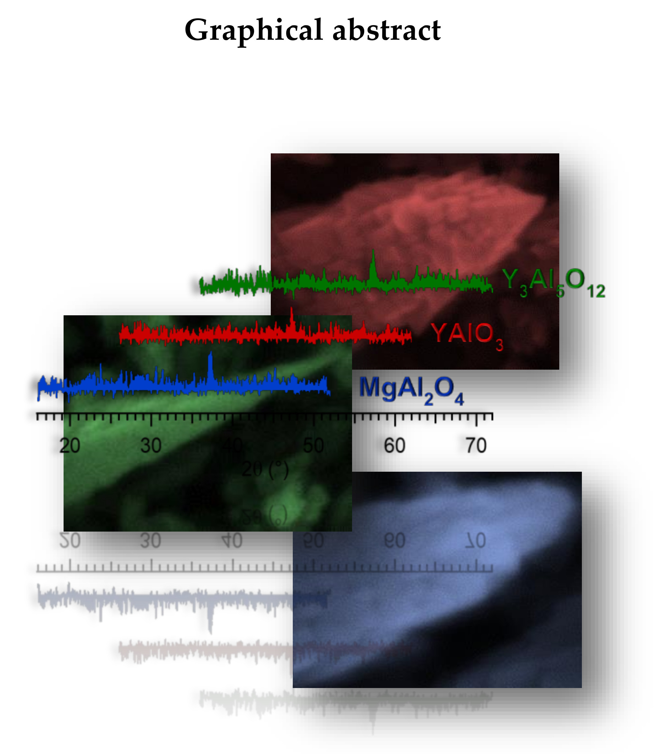
Plasma-Assisted Chemical Vapor Deposition of F-Doped MnO2 Nanostructures on Single Crystal Substrates

1
Department of Chemical Sciences, Padova University and INSTM, 35131 Padova, Italy
2
Department of Physics and Astronomy, Padova University and INSTM, 35131 Padova, Italy
3
Chemistry for Technologies Laboratory, Department of Mechanical and Industrial Engineering, Brescia University and INSTM, 25123 Brescia, Italy
4
CNR-ICMATE and INSTM, Department of Chemical Sciences, Padova University, 35131 Padova, Italy
*
Author to whom correspondence should be addressed.
Nanomaterials 2020, 10(7), 1335; https://doi.org/10.3390/nano10071335
Submission received: 3 June 2020 / Revised: 2 July 2020 / Accepted: 4 July 2020 / Published: 8 July 2020

Abstract

:
MnO2 nanostructures were fabricated by plasma assisted-chemical vapor deposition (PA-CVD) using a fluorinated diketonate diamine manganese complex, acting as single-source precursor for both Mn and F. The syntheses were performed from Ar/O2 plasmas on MgAl2O4(100), YAlO3(010), and Y3Al5O12(100) single crystals at a growth temperature of 300 °C, in order to investigate the substrate influence on material chemico-physical properties. A detailed characterization through complementary analytical techniques highlighted the formation of highly pure and oriented F-doped systems, comprising the sole β-MnO2 polymorph and exhibiting an inherent oxygen deficiency. Optical absorption spectroscopy revealed the presence of an appreciable Vis-light harvesting, of interest in view of possible photocatalytic applications in pollutant degradation and hydrogen production. The used substrates directly affected the system structural features, as well as the resulting magnetic characteristics. In particular, magnetic force microscopy (MFM) measurements, sensitive to the out-of-plane magnetization component, highlighted the formation of spin domains and long-range magnetic ordering in the developed materials, with features dependent on the system morphology. These results open the door to future engineering of the present nanostructures as possible magnetic media for integration in data storage devices.

Graphical Abstract

1. Introduction

Manganese oxides have attracted considerable interest thanks to their diversity of oxidation states and crystal structures, yielding broadly tunable characteristics as a function of the adopted preparation conditions [1,2,3,4,5,6,7,8,9,10,11]. In particular, a remarkable attention has been focused on manganese dioxide, thanks to its low-cost, natural abundance, environmental friendliness, and versatile chemico-physical properties [12,13,14,15]. MnO2 exhibits at least six different structurally related crystalline modifications (α, β, γ, δ, ε, and λ) [1,2,4,7,10,16,17,18,19]. All these polymorphs are semiconductors with low resistivity [2,20,21], and have emerged as attractive candidates for several end-uses, including electrodes in Li- and Na-ion batteries and supercapacitors, thermoelectric materials, chemical sensors, photo- and electrocatalysts for pollutant degradation and hydrogen production, and magnetic devices useful for information storage [5,8,11,12,13,14,15,18,21,22,23,24,25,26,27,28,29,30,31,32,33]. Among MnO2 polymorphs, the most stable and abundant, i.e., rutile-type β-MnO2 (pyrolusite) [16,34,35], is composed of MnO6 octahedra linked by corner-shared oxygens into tunnel-containing frameworks [4,9,23,36]. Amid the various applications, the interest in β-MnO2 has been promoted by its screw-type magnetic structure with an important spin-lattice coupling, as well as by the large room temperature magnetoresistance and ferromagnetism. Altogether, these features are of considerable importance from both a fundamental and a technological point of view, since they can give rise to applications in recording devices and contribute to new studies on electronic-magnetic interactions in the target systems [16,24,25,35,37].
Whereas bulk manganese oxide crystals and, especially, powdered materials with different morphologies have been widely investigated [3,12,16,17,27,29,35,37,38], the fabrication and tailoring of supported thin films and nanostructures, that may yield significant changes in the system behavior, deserves further attention [6,14,15,22]. In this regard, one of the valuable means to modulate MnO2 nanosystem properties involves its controlled anionic doping, far less explored than the conventional cationic one. In particular, fluorine doping can be a useful tool to enhance the surface reactivity and tune both electrical and optical characteristics, a key issue for eventual photocatalytic, energy storage, and gas sensing applications [34,39,40,41,42]. In addition, the obtained system characteristics are directly affected by the electronic structure and properties of surfaces and interfaces, as well as on the nature of the used deposition substrate, which may influence the nucleation kinetics and the subsequent structural and morphological evolution [3,21]. So far, the preparation of MnO2 thin films/nanosystems has been performed on polycrystalline substrates by various techniques. These include reactive sputtering on Si [22], pulsed laser deposition on stainless steel [30], thermal evaporation on glass and quartz [9], hydrothermal routes on Si, carbon cloth, and Ni foams [14,33,43], electrodeposition on stainless steel, glass, carbon fibers, and Ni sheets [7,8,10,11], chemical bath deposition on stainless steel [13,30], spray pyrolysis on glass and steel [15], atomic layer deposition on Si [6,31,32], and chemical vapor deposition (CVD) on Si and glass [23,34,44]. Nevertheless, the use of single crystal substrates can not only stabilize specific polymorphs, but also affect morphology, structure, and crystal quality [21,41,42,45]. To date, different studies have reported on the atomic layer deposition (ALD) of α-MnO2 on NaCl(100), KCl(100), and KBr(100) and of ε-MnO2 on Al2O3(001) [1,21]. In addition, λ-MnO2 films have been grown on MgO(001) by plasma assisted-molecular beam epitaxy (PA-MBE) [26,27]. Films of the most stable β-MnO2 polymorph have been obtained by ALD on Al2O3(012), SiO2(001), and MgO(100) [1,2,21] by PA-MBE on Si(100), MgO(001), TiO2(110), and LaAlO3(001) [4,20,24,25,28], and by pulsed laser deposition (PLD) on Si(100) [5]. Nevertheless, various of these processes involved relatively harsh conditions either in terms of reaction atmosphere (e.g., use of ozone [1,2,6,21,31,32]) or of the used power/temperature [4,5,24,25,27,28,30]. In view of possible practical applications, the availability and implementation of milder and flexible preparative procedures enabling a good control over material structure, morphology, and functional properties represent an important requirement [45].
In this study, F-doped β-MnO2 nanostructures are deposited on MgAl2O4(100), YAlO3(010), and Y3Al5O12(100) single crystals, investigating the substrate influence on the resulting material chemico-physical properties. To the best of our knowledge, none of these substrates has ever been utilized so far for the growth of MnO2 thin films/nanostructures. For the first time, the target nanosystems are prepared by means of plasma assisted-CVD (PA-CVD), exploiting the inherent advantages and versatility of this technique for the tailored fabrication of supported materials under relatively soft operating conditions [34,45]. Mn(hfa)2TMEDA (Hhfa = 1,1,1,5,5,5-hexafluoro-2,4-pentanedione; TMEDA = N,N,N′,N′-tetramethylethylenediamine) [44,46], a fluorinated molecular compound, was used as a single-source precursor for both Mn and F. The obtained nanomaterials were analyzed by a multi-technique approach, involving X-ray photoelectron spectroscopy (XPS), secondary ion mass spectrometry (SIMS), field emission-scanning electron microscopy (FE-SEM), X-ray diffraction (XRD), and optical absorption measurements. In addition, the system surface morphology and magnetic characteristics were investigated by the combined use of atomic force microscopy (AFM) and magnetic force microscopy (MFM), a valuable analytical tool for the local investigation of magnetic properties [47,48,49,50].

2. Experimental Procedure

2.1. Synthesis

MnO2 depositions were performed using a custom-built, two-electrode plasmochemical instrumentation equipped with a radio frequency (RF) generator (ν = 13.56 MHz). In each experiment, one of the target single crystals (MgAl2O4(100), YAlO3 (010), and Y3Al5O12(100), CRYSTAL GmbH®, Berlin, 10 × 10 × 1 mm3, one-side polished) was fixed on the grounded electrode and used as growth substrate without any pre-treatment. The Mn(hfa)2TMEDA precursor powders (0.20 g for each deposition), synthesized according to the literature [44,46], were placed in an external glass vessel heated at 70 °C and transported into the deposition zone by an Ar flow (rate = 60 standard cubic centimeters per minute (sccm)). In order to avoid detrimental condensation phenomena, with consequent mass losses, the gas lines connecting the precursor reservoir and the reaction chamber were maintained at 130 °C throughout each experiment. Two separate auxiliary gas lines were used to introduce Ar (15 sccm) and O2 (5 sccm) directly into the reactor. Basing on previous experiments, the RF-power, total pressure, and interelectrode distance were kept constant at 20 W, 1.0 mbar, and 6 cm. Depositions were performed, for each of the three substrates, at a fixed growth temperature of 300 °C and for a duration of 90 min. Repeated growth experiments under the same conditions enabled to ascertain the full reproducibility of material chemico-physical characteristics. The use of higher growth temperatures was avoided in order to prevent MnO2 transformation into Mn2O3 or Mn3O4 [22,28,30,36]. For the same reason, the obtained samples were analyzed as-prepared, without any ex-situ thermal treatment.

2.2. Characterization

XPS analyses were performed using a Perkin–Elmer (Chanhassen, MN, USA) Φ 5600ci spectrometer, using a non-monochromatized Al Kα X-ray excitation source ( = 1486.6 eV), at working pressures lower than 10−8 mbar. Binding energy (BE) values were corrected for charging by assigning a value of 284.8 eV to the adventitious C1s signal. Atomic percentages (at.%) were calculated by signal integration using standard Φ V5.4A sensitivity factors. Peak fitting was performed through a least-squares procedure using the XPSPEAK program [51], with Gaussian–Lorentzian sum functions. Ar+ sputtering was performed at 3.5 kV (Ar partial pressure = 5 × 10⁻⁸ mbar).
SIMS analyses were carried out at pressures lower than 1 × 10⁻⁹ mbar by means of a Cameca (Gennevilliers, CEDEX, France) IMS 4f spectrometer, using a Cs+ primary ion beam (14.5 keV, 20 nA, stability 0.1%) and negative secondary ion detection. The profiles were recorded adopting an electron gun for charge compensation, rastering over a 175 × 175 μm2 area and detecting secondary ions from a 8 × 8 μm2 sub-region in order to avoid crater effects. Signals were collected in beam blanking mode and high mass resolution configuration. Sputtering times were converted into depth using the nanodeposit thickness values measured by FE-SEM measurements.
Plane-view and cross-sectional FE-SEM analyses were carried out on a Zeiss (Oberkochen, Germany) SUPRA 40VP apparatus, at a primary beam acceleration voltage of 5.0 kV. Nanoaggregate dimensions and deposit thickness values were obtaining through the ImageJ® software [52] by averaging over various independent measurements.
XRD patterns were collected by means of a Bruker (Billerica, MA, USA) D8 Advance diffractometer equipped with a Göbel mirror, using a Cu Kα X-ray source (40 kV, 40 mA). The average crystallite sizes D were calculated from the recorded patterns using the Scherrer formula [15,18,53]:
D = 0.9 [λ/(FWHM × cosθ)]
where λ = 0.15418 nm for the Cu Kα X-ray source, whereas FWHM and 2θ are the peak full width at half maximum and angular position, respectively. In this work, the calculation was performed on the (101) β-MnO2 reflection [54], from which dislocation density (δ) and microstrain (ε) values were estimated through the following equations [19,34]:
δ = 1/D2
ε = FWHM/(4 × tgθ)
Optical absorption spectra were recorded in transmittance mode at normal incidence on a Cary 50 (Agilent, Santa Clara, CA, USA) spectrophotometer, subtracting the substrate contribution in each case. Estimation of band gap (EG) values was performed through the Tauc procedure [7,8,9,30,46,48]:
(αhν)n = A(EG)
where α is the absorption coefficient, is the photon energy, A is a constant, and n is a coefficient dependent on the nature of the occurring electronic transitions (n = 2 for direct and allowed electronic transitions [15,18,23]). EG values were obtained by extrapolating the experimental curves to intersect the horizontal energy axis at α = 0.
AFM and MFM analyses were performed using a NT-MDT (Moscow, Russia) SPM Solver P47H–PRO apparatus, operating in tapping mode and in air at atmospheric pressure. Root-mean-square (RMS) surface roughness values were obtained from 3 × 3 μm2 micrographs by the NT-MDT software, after plane fitting. MFM analyses were carried out using commercial cantilever tips (average height = 15 µm) coated with a CoCr magnetic layer, pre-magnetized by means of an external field. The magnetic force was measured by monitoring phase shifts in cantilever oscillations determined by tip-specimen magnetic interactions. The possible influence of electrostatic interactions was reduced by sample discharging prior to each analysis.

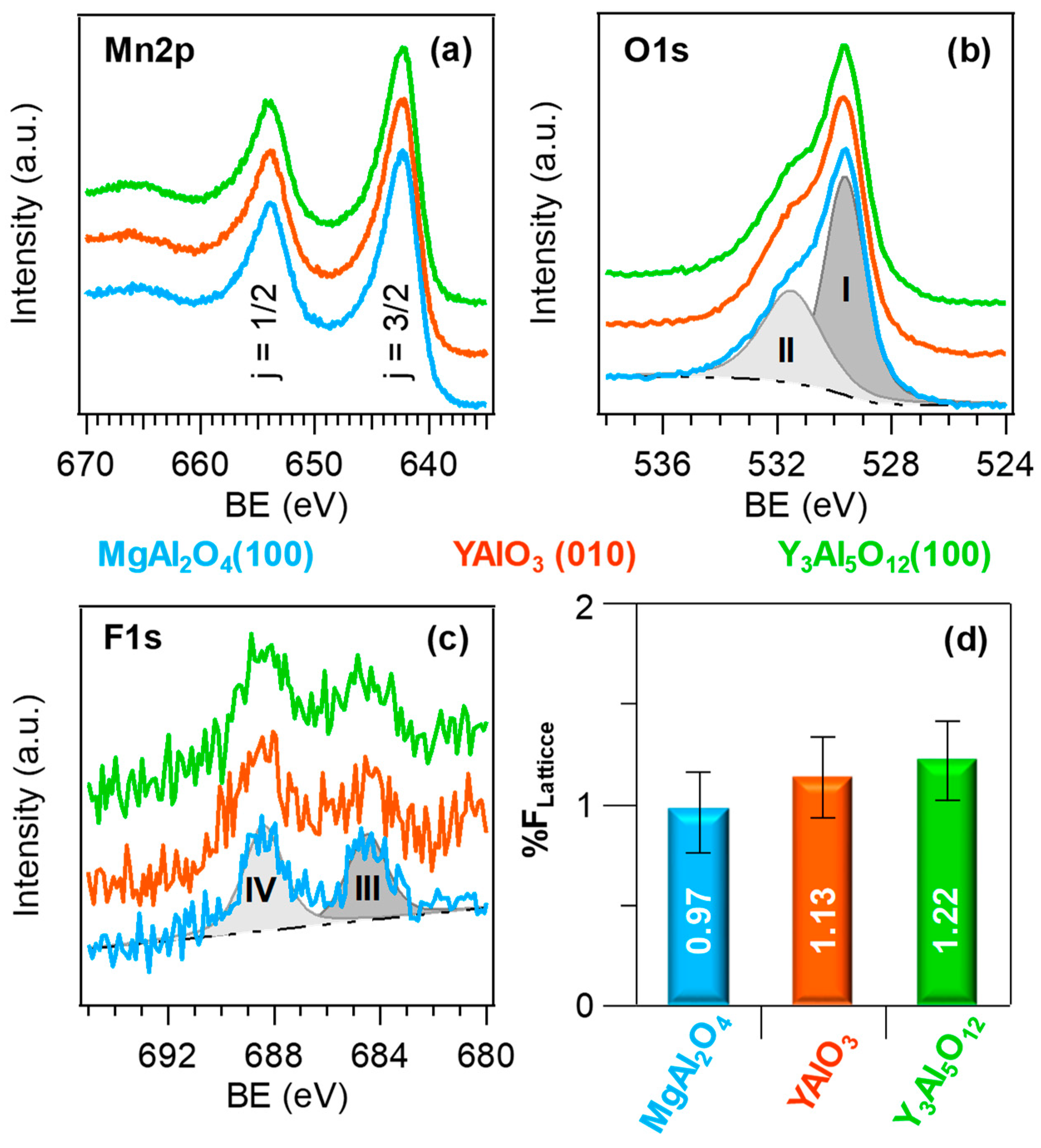
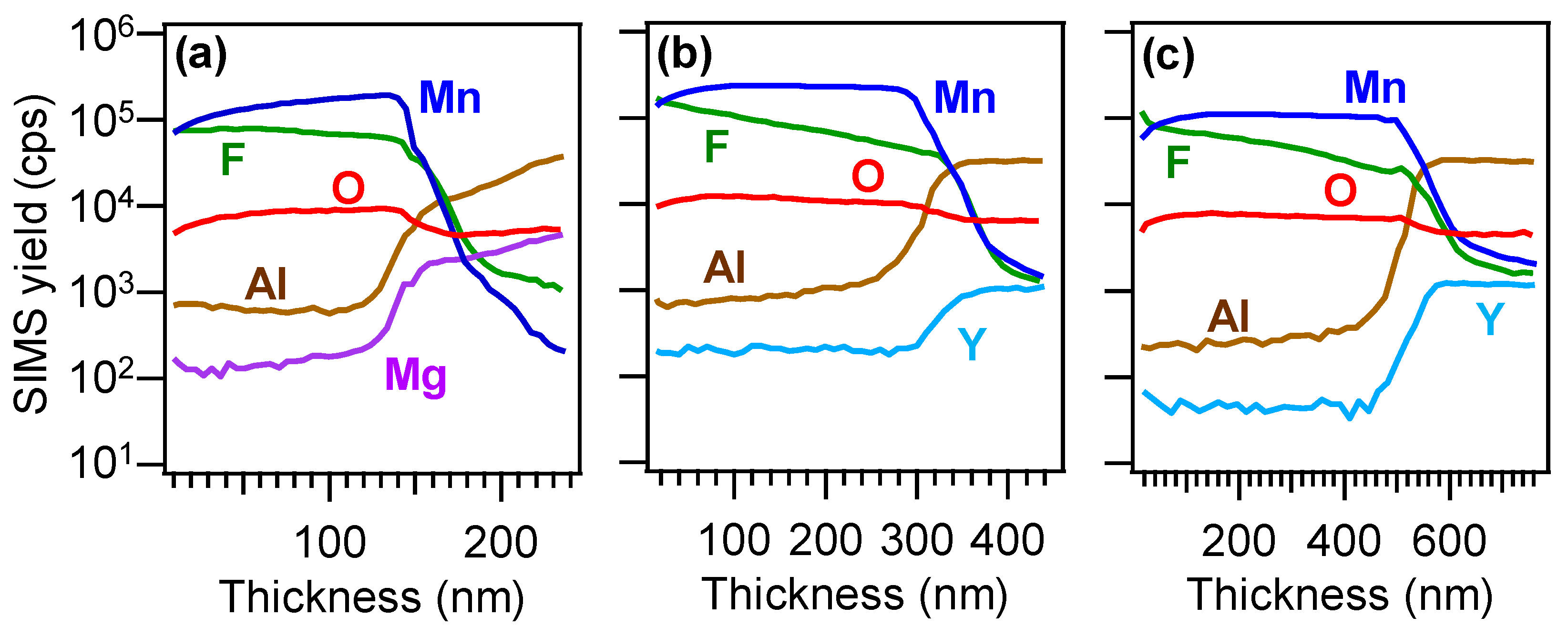
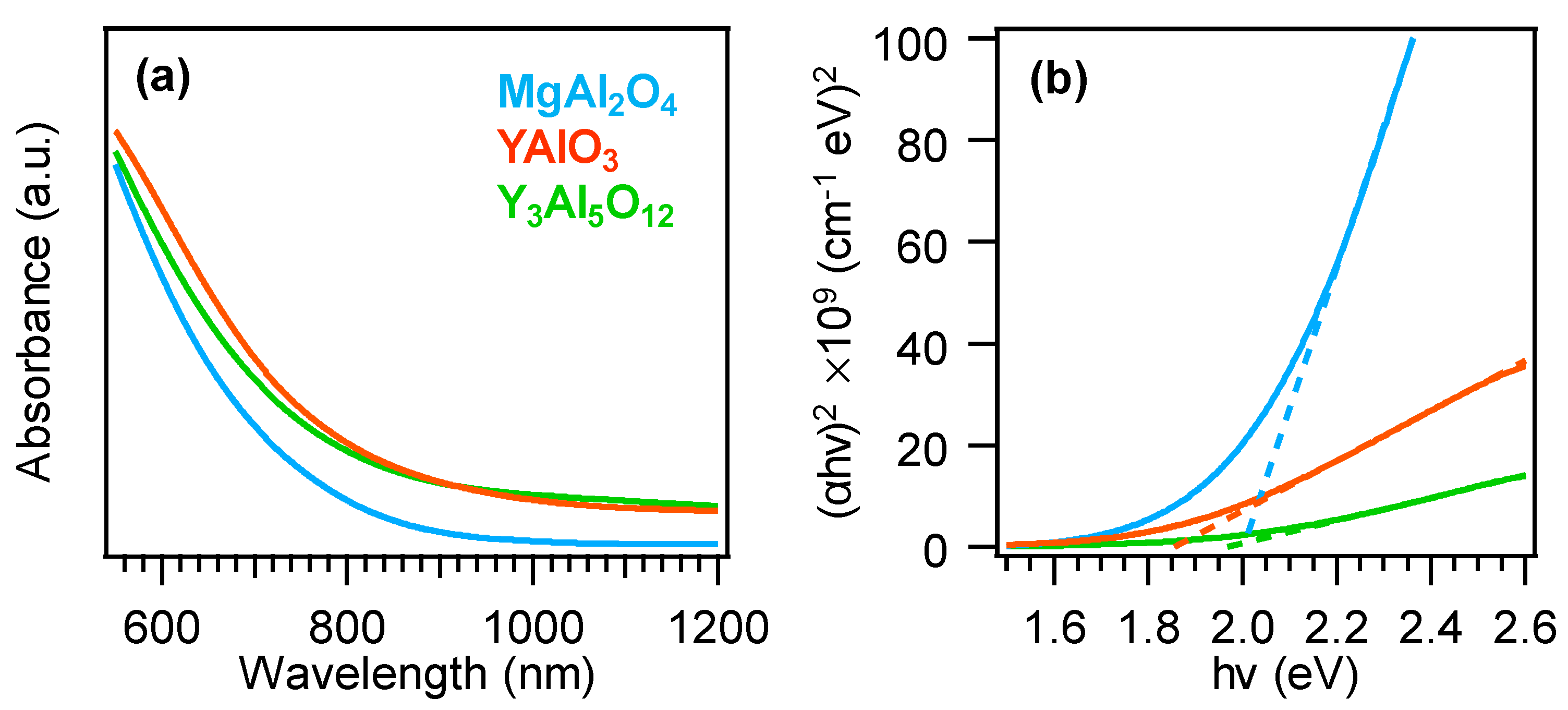
3. Results and Discussion

The surface chemical states of the developed materials were characterized by XPS. For all the analyzed systems, only manganese, oxygen, fluorine, and carbon peaks were present in the survey scans (see Figure S1a). The disappearance of C signals upon Ar+ sputtering for 10 min highlighted the good system purity. In all cases, the presence of pure MnO2 was testified by the Mn2p signal shape and position (BE(Mn2p3/2) = 642.4 eV, spin-orbit separation = 11.6 eV; see Figure 1a) [4,10,14,28,44], as well as by the Mn3s multiplet splitting separation (Figure S1b). In fact, when the 3s electron is photoejected from a paramagnetic center like manganese, the exchange coupling between the 3s hole created after photoemission and the 3d electrons results in a signal splitting, whose magnitude is a fingerprint of the metal oxidation state [3,6,8,44]. In the present case, the obtained separation value was 4.7 eV, in good agreement with literature values for MnO2 [2,11,23,34], confirming thus the absence of other manganese oxides in the analyzed nanomaterials. The latter conclusion was further corroborated by the energy difference between the Mn2p3/2 and O1s lattice components (112.7 eV; see below) [23,32,34]. In fact, two components contributed to the O1s signal (Figure 1b and Figure S2a–c), a major one at 529.6 eV (I), attributed to lattice Mn–O–Mn moieties, and a second one at higher BE (II), centered at 531.5 eV, due to the presence of hydroxyl groups/oxygen chemisorbed on surface O defects [13,39,42,43]. The occurrence of the latter, already reported in previous literature studies on various manganese dioxide polymorphs [8,16,25,37], is in line with optical absorption results (see below). The surface F1s signal (Figure 1c,d, Figures S1c and S2d–f) was deconvoluted by means of two different bands, located at 684.6 eV (III) and 688.5 eV (IV). Component (III) was ascribed to lattice fluorine incorporated in manganese dioxide network, i.e., to Mn-F bonds, whereas the higher BE band (IV) located at BE = 688.5 eV was due to CFx groups from precursor residuals [34,39,41,44]. Whereas band (III) was present even in the inner deposit region, band (IV) was reduced to noise level after 10 min of Ar+ erosion, indicating that, as already observed for carbon signals, contaminating species were limited to the system surface.
Important information on the in-depth composition was gained by SIMS profiling (Figure 2a–c), that revealed a good material purity (mean C content lower than 10 ppm). The results highlighted an even F distribution throughout the investigated thickness, confirming a successful fluorine incorporation into manganese dioxide network. This phenomenon was traced back to the production of F• radicals deriving from precursor fragmentation in the used plasmas [34,39,40]. The almost parallel trends of manganese and oxygen signals indicated a homogeneous composition, in line with the presence of pure manganese(IV) oxide. The broadened deposit/substrate interface was related to the nano-organization of the developed systems, as revealed by FE-SEM analyses (Figure 3a–f). The recorded micrographs evidenced in fact a very open morphology, characterized by the presence of interconnected and anisotropic dendritic structures (mean width ≈ 80 nm) uniformly protruding from the underlying substrate surface. Such features might be beneficial for possible end-uses in photocatalysis [7,19,23,34,39,44], with particular regard to wastewater purification from organic pollutants and to water splitting for hydrogen production. The average length of the observed dendrites was directly affected by the used deposition substrate (220 nm, MgAl2O4(100); 200 nm, YAlO3(010); 270 nm, Y3Al5O12(010)). The observed nanoaggregates originated, in turn, from the assembly of smaller nanograins, whose dimensions, for each sample, were very close to those of the corresponding crystallites calculated by XRD analyses (see below and Figure S3). The mean deposit thickness values were estimated to be 230, 330, and 550 nm for nanomaterials supported on MgAl2O4(100), YAlO3(010), and Y3Al5O12(100). The obtainment of these different values suggested a remarkable substrate influence on precursor decomposition and nanosystem growth, all the other conditions being constant (see the Experimental section).
The system structure was investigated by XRD (Figure 4a). All the recorded patterns were characterized by a single reflection located at 2θ = 37.3°, related to the (101) crystallographic planes of tetragonal β-MnO2 (pyrolusite; space group = P42/mnm; a = b = 4.40 Å and c = 2.87 Å [1,4,16,21,35,37]). The presence of the sole (101) reflection irrespective of the used substrate suggested the occurrence of a (101) preferential orientation and/or of anisotropic crystallite growth [23,34,44]. The relatively weak and broad diffraction peaks, as often observed in the case of supported MnO2 films/nanosystems [9,10,13,14,22,33], suggested the formation of defective nanocrystallites, whose average dimensions were comprised between 25 and 35 nm (Figure S3).
The calculated dislocation density (δ) and microstrain (ε) values for the present materials (Figure 4b,c) were smaller than those reported for Si-supported MnO2 nanosystems [34]. In line with previous studies [19,42,55], the higher δ and ε values for the specimen supported on Y3Al5O12(100) corresponded to lower crystallite size dimensions (see Figure S3). This result was ascribed to the different lattice mismatch between MnO2 and the used substrates, highlighting the influence of the latter on the structural characteristics of the obtained systems and suggesting a lower content of dislocations and defects for materials supported on YAlO3.
Subsequently, attention was dedicated to the analysis of the system optical properties. All the recorded optical absorption spectra (Figure 5a) were characterized by a prominent absorption for wavelengths lower than 700 nm, corresponding to interband electronic transitions [8,23]. The broadened absorption towards the near-IR region was consistent with the presence of oxygen vacancies, as indicated by XPS analyses (see above). As a matter of fact, the occurrence of oxygen defects in the target nanomaterials can favorably influence the system functional behavior for (photo)catalytic end-uses [23,34]. In particular, the present Vis-light harvesting might be beneficial for eventual photocatalytic applications for environmental protection and energy production, as already mentioned [40,42,48]. Irrespective of the substrate nature, Tauc plot analysis (see Figure 5b) yielded a mean energy gap value of EG = (2.0 ± 0.1) eV, which was blue-shifted with respect to that reported for various MnO2 polymorphs [7,9,23]. The occurrence of this phenomenon could be mainly traced back to oxygen replacement by lattice fluorine [23,41], and the almost identical band gap values were in line with the very similar fluorine contents for the present samples (see Figure 1d).
Finally, material surface topography and magnetic properties were investigated by the combined use of AFM and MFM [56,57]. AFM micrographs in Figure 6, left column evidenced a uniform interconnection of tiny aggregates for samples grown on MgAl2O4(100) and Y3Al5O12(100). In line with FE-SEM and XRD results (see Figure 3a–f and Figure S3), the use of YAlO3(010) substrate resulted in the formation of larger agglomerates and a more open morphology with a slightly higher RMS roughness, corresponding to an increased surface area [23,34]. Nonetheless, a detailed analysis of AFM images evidenced a grouping of the dendritic structures observed in FE-SEM ones, related to the tip inability to spatially resolve the single structures [34].
As a matter of fact, MFM analyses probe the perpendicular component of the magnetic stray field from the target systems [58]. As the magnetic tip scans over a multi-domain surface, the variations in the local magnetic stray field can attract or repel the tip, resulting thus in the contrast of the output image, which reflects the spatial distribution of magnetic domains [47,48,53]. As can be observed in Figure 6, right column, the recorded micrographs revealed an even in-plane distribution of magnetic domains. The reversing of MFM contrast from bright to dark can be associated to the switch from repulsive to attractive surface-tip interactions, corresponding, in turn, to upward and downward orientations of magnetic moments, respectively [42]. The lack of single-color large areas enabled to discard the presence of magnetic impurities in appreciable amounts, confirming thus the obtainment of pure MnO2 nanostructures with homogeneous characteristics.
A more detailed inspection of MFM micrographs revealed the occurrence of a multi-domain configuration directly dependent on the growth substrate. For the Y3Al5O12(100)-supported sample, the dimensions of magnetic domains (DMFM) and of the aggregates probed by AFM (DAFM) were comparable (DMFMDAFM). In a different way, DMFM was higher (lower) than DAFM for deposits supported on MgAl2O4(100) (YAlO3(010)). This result indicated that, in the former case, magnetic domains were formed by different aggregates with an analogous alignment [34], while in the latter magnetic domains were separated by less abrupt walls.
Taken together, the results yielded by MFM analysis highlight the stability of the system magnetization down to the nanoscale, with tailored magnetic features and a long-range magnetic ordering. These evidences candidate the target materials for use in data storage devices. Nevertheless, the quantitative analysis of magnetic properties by the sole use of MFM is a difficult task, since the obtained magnetic signals can be overlapped with additional forces acting on the tip, such as electrostatic ones, resulting in the occurrence of topographic features in MFM images. Furthermore, as mentioned above, MFM signals are highly sensitive only to the out-of-plane magnetic stray field, preventing a straightforward prediction of a full 3D magnetic configuration [49]. Overall, these issues highlight the importance of additional analyses by complementary techniques [50] for a more detailed investigation of material magnetic properties and for further applicative research developments along this direction.

4. Conclusions

In summary, highly pure and oriented manganese(IV) oxide nanostructures were grown on MgAl2O4(100), YAlO3(010), and Y3Al5O12(100) single crystal substrates by PA-CVD. The obtained systems, grown under milder operating conditions with respect to various literature works, were characterized by the presence of single-phase, O-deficient β-MnO2 polymorph, the most stable and abundant one belonging to the manganese dioxide family. The use of a fluorinated molecular precursor, acting as a single-source for both Mn and F, enabled to obtain an in-situ doping of the prepared systems, with an even fluorine incorporation throughout the deposit thickness. The target materials yielded appreciable radiation absorption in the Vis spectral range, an important pre-requisite for their possible use in photocatalytic applications, such as water splitting to yield hydrogen and organic pollutant decomposition for wastewater purification. The combined use of XRD, FE-SEM, and AFM techniques evidenced that structural and morphological characteristics were directly affected by the used growth substrate. The latter also directly influenced the local variance of signals in MFM, whose utilization revealed the obtainment of spin domains with a long-range magnetic ordering, of possible interest for material application as magnetic media for integration in data storage devices. In this regard, one of the most interesting perspectives for future developments of the present work would concern a deeper investigation of the system magnetic properties as a function of fluorine content by means of complementary techniques. In addition, the outcomes yielded by this study may open up attractive perspectives for the translation of the proposed preparation route to thin films and nanosystems with a memory function for recording devices, in which reading and writing of data can be done by magneto-optical effect.

Supplementary Materials

The following are available online at https://www.mdpi.com/2079-4991/10/7/1335/s1: Figure S1: XPS survey spectra, Mn3s signals, and total surface fluorine content for MnO2 samples. Figure S2: Deconvolution of surface O1s and F1s XP spectra for the target specimens. Figure S3: Mean crystallite size values for the analyzed samples.

Author Contributions

Conceptualization, L.B., C.M., and D.B.; data curation, L.B.; formal analysis, A.G., C.S., and E.B.; funding acquisition, A.G.; investigation, L.B., C.S., and C.M.; project administration, C.M.; resources, C.M.; validation, D.B. and E.B.; writing—original draft, D.B.; writing—review and editing, A.G. and E.B. All authors have read and agreed to the published version of the manuscript.

Funding

The present work was financially supported by Padova University DOR 2016–2019 and P-DiSC #SENSATIONAL BIRD2016-UNIPD and #03BIRD2018 OXYGENA projects, as well as by AMGA Foundation Mn4Energy project and by the INSTM Consortium (INSTMPD004—NETTUNO and INSTMPD010—ISIDE).

Conflicts of Interest

The authors declare no conflict of interest.

References and Note

  1. Foss, S.; Nilsen, O.; Olsen, A.; Taftø, J. Structure determination of MnO2 films grown on single crystal α-Al2O3 substrates. Philos. Mag. 2005, 85, 2689–2705. [Google Scholar] [CrossRef]
  2. Nilsen, O.; Fjellvåg, H.; Kjekshus, A. Growth of manganese oxide thin films by atomic layer deposition. Thin Solid Films 2003, 444, 44–51. [Google Scholar] [CrossRef]
  3. Ren, L.; Wu, S.; Zhou, W.; Li, S. Epitaxial growth of manganese oxide films on MgAl2O4 (001) substrates and the possible mechanism. J. Cryst. Growth 2014, 389, 55–59. [Google Scholar] [CrossRef]
  4. Chambers, S.A.; Liang, Y. Growth of β-MnO2 films on TiO2(110) by oxygen plasma assisted molecular beam epitaxy. Surf. Sci. 1999, 420, 123–133. [Google Scholar] [CrossRef]
  5. Abi-Akl, M.; Tabbal, M.; Kassem, W. Crystalline phase control and growth selectivity of β-MnO2 thin films by remote plasma assisted pulsed laser deposition. Thin Solid Films 2016, 612, 450–455. [Google Scholar] [CrossRef]
  6. Li, Y.W.; Qiao, Q.; Zhang, J.Z.; Hu, Z.G.; Chu, J.H. Influence of post-annealing on structural, electrical and optical properties of manganese oxide thin films grown by atomic layer deposition. Thin Solid Films 2015, 574, 115–119. [Google Scholar] [CrossRef]
  7. Moulai, F.; Fellahi, O.; Messaoudi, B.; Hadjersi, T.; Zerroual, L. Electrodeposition of nanostructured γ-MnO2 film for photodegradation of Rhodamine B. Ionics 2018, 24, 2099–2109. [Google Scholar] [CrossRef]
  8. Pinaud, B.A.; Chen, Z.B.; Abram, D.N.; Jaramillo, T.F. Thin films of sodium birnessite-type MnO2: Optical properties, electronic band structure, and solar photoelectrochemistry. J. Phys. Chem. C 2011, 115, 11830–11838. [Google Scholar] [CrossRef]
  9. Makhlouf, M.M. Preparation and optical characterization of β-MnO2 nano thin films for application in heterojunction photodiodes. Sens. Actuators A 2018, 279, 145–156. [Google Scholar] [CrossRef]
  10. Chou, S.L.; Cheng, F.Y.; Chen, J. Electrodeposition synthesis and electrochemical properties of nanostructured γ-MnO2 films. J. Power Sources 2006, 162, 727–734. [Google Scholar] [CrossRef]
  11. Chen, Y.; Hu, W.; Gan, H.; Wang, J.-W.; Shi, X.-C. Enhancing high-rate capability of MnO2 film electrodeposited on carbon fibers via hydrothermal treatment. Electrochim. Acta 2017, 246, 890–896. [Google Scholar] [CrossRef]
  12. Wan, X.; Yang, S.; Cai, Z.; He, Q.; Ye, Y.; Xia, Y.; Li, G.; Liu, J. Facile synthesis of MnO2 nanoflowers/N-doped reduced graphene oxide composite and its application for simultaneous determination of dopamine and uric acid. Nanomaterials 2019, 9, 847. [Google Scholar] [CrossRef] [PubMed] [Green Version]
  13. Patil, A.M.; Lokhande, V.C.; Patil, U.M.; Shinde, P.A.; Lokhande, C.D. High performance all-solid-state asymmetric supercapacitor device based on 3D nanospheres of β-MnO2 and nanoflowers of O-SnS. ACS Sustainable Chem. Eng. 2018, 6, 787–802. [Google Scholar] [CrossRef]
  14. Shinde, P.A.; Lokhande, V.C.; Ji, T.; Lokhande, C.D. Facile synthesis of hierarchical mesoporous weirds-like morphological MnO2 thin films on carbon cloth for high performance supercapacitor application. J. Colloid Interface Sci. 2017, 498, 202–209. [Google Scholar] [CrossRef]
  15. Balamurugan, S.; Rajalakshmi, A.; Balamurugan, D. Acetaldehyde sensing property of spray deposited β-MnO2 thin films. J. Alloys Compd. 2015, 650, 863–870. [Google Scholar] [CrossRef]
  16. Luo, F.; Song, W.; Yan, C.-H. Enhanced room temperature magnetoresistance effect in oxygen defective β-MnO2 microcrystal. Chem. Phys. Lett. 2006, 431, 337–340. [Google Scholar] [CrossRef]
  17. Kim, H.; Lee, J.; Kim, Y.-M.; Jung, M.-H.; Jagličić, Z.; Umek, P.; Dolinšek, J. Synthesis, structure and magnetic properties of β-MnO2 nanorods. Nanoscale Res. Lett. 2007, 2, 81. [Google Scholar] [CrossRef] [Green Version]
  18. Awad, M.A.; Hadia, N.M.A. Towards understanding the morphological, magnetic, optical and electrical properties of MnO2 nanowires for magneto- and optoelectronic applications. J. Mater. Sci. Mater. Electron. 2018, 29, 20695–20702. [Google Scholar] [CrossRef]
  19. Ramesh, M.; Nagaraja, H.S.; Rao, M.P.; Anandan, S.; Huang, N.M. Fabrication, Characterization and Catalytic Activity of α-MnO2 Nanowires for Dye Degradation of Reactive Black 5. Mater. Lett. 2016, 172, 85–89. [Google Scholar] [CrossRef]
  20. Yu, X.L.; Wu, S.X.; Liu, Y.J.; Li, S.W. Electronic spectrum of a helically Hund-coupled β-MnO2. Solid State Commun. 2008, 146, 166–168. [Google Scholar] [CrossRef]
  21. Nilsen, O.; Foss, S.; Fjellvåg, H.; Kjekshus, A. Effect of substrate on the characteristics of manganese(IV) oxide thin films prepared by atomic layer deposition. Thin Solid Films 2004, 468, 65–74. [Google Scholar] [CrossRef]
  22. Music, D.; Bliem, P.; Geyer, R.W.; Schneider, J.M. Atomistic growth phenomena of reactively sputtered RuO2 and MnO2 thin films. J. Appl. Phys. 2015, 118, 015302. [Google Scholar] [CrossRef]
  23. Barreca, D.; Gri, F.; Gasparotto, A.; Carraro, G.; Bigiani, L.; Altantzis, T.; Žener, B.; Lavrenčič Štangar, U.; Alessi, B.; Padmanaban, D.B.; et al. Multi-Functional MnO2 nanomaterials for photo-activated applications by a plasma-assisted fabrication route. Nanoscale 2019, 11, 98–108. [Google Scholar] [CrossRef] [PubMed] [Green Version]
  24. Yu, X.L.; Chen, J.; Wu, S.X.; Liu, Y.J.; Li, S.W. Polarized Raman scattering in helimagnetic β-MnO2. J. Raman Spectrosc. 2008, 39, 1440–1443. [Google Scholar] [CrossRef]
  25. Xing, X.J.; Yu, Y.P.; Xu, L.M.; Wu, S.X.; Li, S.W. Magnetic properties of β-MnO2 thin films grown by plasma-assisted molecular beam epitaxy. J. Phys. Chem. C 2008, 112, 15526–15531. [Google Scholar] [CrossRef]
  26. Guo, L.W.; Peng, D.L.; Makino, H.; Hanada, T.; Hong, S.K.; Sumiyama, K.; Yao, T.; Inaba, K. Structural characteristics and magnetic properties of λ-MnO2 films grown by plasma-assisted molecular beam epitaxy. J. Appl. Phys. 2001, 90, 351–354. [Google Scholar] [CrossRef]
  27. Guo, L.W.; Makino, H.; Ko, H.J.; Chen, Y.F.; Hanada, T.; Peng, D.L.; Inaba, K.; Yao, T. Structural characteristic and magnetic properties of Mn oxide films grown by plasma-assisted MBE. J. Cryst. Growth 2001, 227–228, 955–959. [Google Scholar] [CrossRef]
  28. Cui, J.; Ji, T.; Nie, T.; Lv, Y.; Yang, S.; Yang, X.; Jiang, Z.; Zou, J. Growth and memory effect of Er-stabilized β-MnO2 films grown on Si substrates. Mater. Res. Express 2014, 1, 036302. [Google Scholar] [CrossRef]
  29. Guo, C.; Ma, H.; Zhang, Q.; Li, M.; Jiang, H.; Chen, C.; Wang, S.; Min, D. Nano MnO2 radially grown on lignin-based carbon fiber by one-step solution reaction for supercapacitors with high performance. Nanomaterials 2020, 10, 594. [Google Scholar] [CrossRef] [Green Version]
  30. Nayak, D.; Ghosh, S.; Adyam, V. Thin film manganese oxide polymorphs as anode for sodium-ion batteries: An electrochemical and DFT based study. Mater. Chem. Phys. 2018, 217, 82–89. [Google Scholar] [CrossRef]
  31. Nieminen, H.-E.; Miikkulainen, V.; Settipani, D.; Simonelli, L.; Hönicke, P.; Zech, C.; Kayser, Y.; Beckhoff, B.; Honkanen, A.-P.; Heikkilä, M.J.; et al. Intercalation of lithium ions from gaseous precursors into β-MnO2 thin films deposited by atomic layer deposition. J. Phys. Chem. C 2019, 123, 15802–15814. [Google Scholar] [CrossRef] [Green Version]
  32. Mattelaer, F.; Bosserez, T.; Ronge, J.; Martens, J.A.; Dendooven, J.; Detavernier, C. Manganese oxide films with controlled oxidation state for water splitting devices through a combination of atomic layer deposition and post-deposition annealing. RSC Adv. 2016, 6, 98337–98343. [Google Scholar] [CrossRef]
  33. Zhu, T.; He, Z.; Zhang, G.; Lu, Y.; Lin, C.; Chen, Y.; Guo, H. Effect of low magnetic fields on the morphology and electrochemical properties of MnO2 films on nickel foams. J. Alloys Compd. 2015, 644, 186–192. [Google Scholar] [CrossRef]
  34. Barreca, D.; Gri, F.; Gasparotto, A.; Altantzis, T.; Gombac, V.; Fornasiero, P.; Maccato, C. Insights into the plasma-assisted fabrication and nanoscopic investigation of tailored MnO2 nanomaterials. Inorg. Chem. 2018, 57, 14564–14573. [Google Scholar] [CrossRef] [PubMed]
  35. Regulski, M.; Przeniosło, R.; Sosnowska, I.; Hoffmann, J.U. Incommensurate magnetic structure of β-MnO2. Phys. Rev. B 2003, 68, 172401. [Google Scholar] [CrossRef]
  36. Ilton, E.S.; Droubay, T.C.; Chaka, A.M.; Kovarik, L.; Varga, T.; Arey, B.W.; Kerisit, S.N. Epitaxial single-crystal thin films of MnxTi1−xO2−δ grown on (rutile)TiO2 substrates with pulsed laser deposition: Experiment and theory. Surf. Sci. 2015, 632, 185–194. [Google Scholar] [CrossRef] [Green Version]
  37. Regulski, M.; Przeniosło, R.; Sosnowska, I.; Hoffmann, J.-U. Short and long range magnetic ordering in β-MnO2-A temperature study -. J. Phys. Soc. Jpn. 2004, 73, 3444–3447. [Google Scholar] [CrossRef]
  38. Guo, X.; Li, J.; Jin, X.; Han, Y.; Lin, Y.; Lei, Z.; Wang, S.; Qin, L.; Jiao, S.; Cao, R. A hollow-structured manganese oxide cathode for stable Zn-MnO2 batteries. Nanomaterials 2018, 8, 301. [Google Scholar] [CrossRef] [Green Version]
  39. Carraro, G.; Gasparotto, A.; Maccato, C.; Bontempi, E.; Lebedev, O.I.; Turner, S.; Sada, C.; Depero, L.E.; Van Tendeloo, G.; Barreca, D. Fluorine doped Fe2O3 nanostructures by a one-pot plasma-assisted strategy. RSC Adv. 2013, 3, 23762–23768. [Google Scholar] [CrossRef]
  40. Gasparotto, A.; Barreca, D.; Bekermann, D.; Devi, A.; Fischer, R.A.; Fornasiero, P.; Gombac, V.; Lebedev, O.I.; Maccato, C.; Montini, T.; et al. F-doped Co3O4 photocatalysts for sustainable H2 generation from water/ethanol. J. Am. Chem. Soc. 2011, 133, 19362–19365. [Google Scholar] [CrossRef]
  41. Carraro, G.; Gasparotto, A.; Maccato, C.; Bontempi, E.; Lebedev, O.I.; Sada, C.; Turner, S.; Van Tendeloo, G.; Barreca, D. Rational synthesis of F-doped iron oxides on Al2O3(0001) single crystals. RSC Adv. 2014, 4, 52140–52146. [Google Scholar] [CrossRef]
  42. Bigiani, L.; Maccato, C.; Gasparotto, A.; Sada, C.; Barreca, D. Structure and properties of Mn3O4 thin films grown on single crystal substrates by chemical vapor deposition. Mater. Chem. Phys. 2019, 223, 591–596. [Google Scholar] [CrossRef] [Green Version]
  43. Yan, D.; Yan, P.X.; Cheng, S.; Chen, J.T.; Zhuo, R.F.; Feng, J.J.; Zhang, G.A. Fabrication, in-depth characterization, and formation mechanism of crystalline porous birnessite MnO2 film with amorphous bottom layers by hydrothermal method. Cryst. Growth Des. 2009, 9, 218–222. [Google Scholar] [CrossRef]
  44. Barreca, D.; Carraro, G.; Fois, E.; Gasparotto, A.; Gri, F.; Seraglia, R.; Wilken, M.; Venzo, A.; Devi, A.; Tabacchi, G.; et al. Manganese(II) molecular sources for plasma-assisted CVD of Mn oxides and fluorides: From precursors to growth process. J. Phys. Chem. C 2018, 122, 1367–1375. [Google Scholar] [CrossRef] [Green Version]
  45. Barreca, D.; Devi, A.; Fischer, R.A.; Bekermann, D.; Gasparotto, A.; Gavagnin, M.; Maccato, C.; Tondello, E.; Bontempi, E.; Depero, L.E.; et al. Strongly oriented Co3O4 thin films on MgO(100) and MgAl2O4(100) substrates by PE-CVD. CrystEngComm 2011, 13, 3670–3673. [Google Scholar] [CrossRef]
  46. Maccato, C.; Bigiani, L.; Carraro, G.; Gasparotto, A.; Seraglia, R.; Kim, J.; Devi, A.; Tabacchi, G.; Fois, E.; Pace, G.; et al. Molecular engineering of MnII diamine diketonate precursors for the vapor deposition of manganese oxide nanostructures. Chem. Eur. J. 2017, 23, 17954–17963. [Google Scholar] [CrossRef]
  47. Hu, S.; Cazorla, C.; Xiang, F.; Ma, H.; Wang, J.; Wang, J.; Wang, X.; Ulrich, C.; Chen, L.; Seidel, J. Strain control of giant magnetic anisotropy in metallic perovskite SrCoO3−δ thin films. ACS Appl. Mater. Interfaces 2018, 10, 22348–22355. [Google Scholar] [CrossRef]
  48. Carraro, G.; Peeters, D.; Gasparotto, A.; Maccato, C.; Bontempi, E.; Barreca, D. Fe2O3 nanostructures on SrTiO3(111) by chemical vapor deposition: Growth and characterization. Mater. Lett. 2014, 136, 141–145. [Google Scholar] [CrossRef]
  49. Rastei, M.V.; Pierron-Bohnes, V.; Toulemon, D.; Bouillet, C.; Kákay, A.; Hertel, R.; Tetsi, E.; Begin-Colin, S.; Pichon, B.P. Defect-driven magnetization configuration of isolated linear assemblies of iron oxide nanoparticles. Adv. Funct. Mater. 2019, 29, 1903927. [Google Scholar] [CrossRef]
  50. Krivcov, A.; Ehrler, J.; Fuhrmann, M.; Junkers, T.; Möbius, H. Influence of dielectric layer thickness and roughness on topographic effects in magnetic force microscopy. Beilstein J. Nanotechnol. 2019, 10, 1056–1064. [Google Scholar] [CrossRef] [Green Version]
  51. Available online: https://xpspeak.software.informer.com/4.1/ (accessed on 20 February 2020).
  52. Available online: http://imagej.nih.gov/ij/ (accessed on 2 April 2020).
  53. Sarilmaz, A.; Ozel, F.; Aljabour, A.; Rauf Khaskheli, A.; Kus, M. Effect of doping on thin film solar cell efficiency based on ZnMn2O4 nanocrystals. Mater. Today Proc. 2019, 18, 1861–1867. [Google Scholar] [CrossRef]
  54. JCPDS card No. 024-0735 (2000) (accessed on 29 April 2020).
  55. Divagar, M.; Sriramprabha, R.; Ponpandian, N.; Viswanathan, C. Highly selective and sensitive electrochemical detection of dopamine with hydrothermally prepared β-MnO2 nanostructures. Mater. Sci. Semicond. Process. 2018, 83, 216–223. [Google Scholar] [CrossRef]
  56. Quiroz, H.P.; Galíndez, E.F.; Dussan, A. Ferromagnetic-like behavior of Co doped TiO2 flexible thin films fabricated via co-sputtering for spintronic applications. Heliyon 2020, 6, e03338. [Google Scholar] [CrossRef] [PubMed] [Green Version]
  57. Quiroz, H.P.; Dussan, A. Synthesis temperature dependence on magnetic properties of cobalt doped TiO2 thin films for spintronic applications. Appl. Surf. Sci. 2019, 484, 688–691. [Google Scholar] [CrossRef]
  58. Tiberto, P.; Barrera, G.; Celegato, F.; Coisson, M.; Olivetti, E.S.; Vinai, F. Microstructural evolution and magnetic properties in Fe50Pd50 sputtered thin films submitted to post-deposition annealing. J. Alloys Compd. 2014, 615, S236–S241. [Google Scholar] [CrossRef]
Figure 1. Core level Mn2p (a), O1s (b), and F1s (c) signals, and lattice fluorine content (d), for manganese dioxide systems deposited on different substrates.
Nanomaterials 10 01335 g001
Figure 2. SIMS depth profiles for the specimens deposited on MgAl2O4(100) (a), YAlO3(010) (b), and Y3Al5O12(100) (c).
Nanomaterials 10 01335 g002
Figure 3. Representative plane-view (left) and cross-sectional (right) FE-SEM images for MnO2 nanostructures grown on MgAl2O4(100) (a,b), YAlO3(010) (c,d), and Y3Al5O12(100) (e,f).
Nanomaterials 10 01335 g003
Figure 4. (a) XRD patterns of MnO2 specimens deposited on different substrates; inset: representation of β-MnO2 structure [54], evidencing (101) crystallographic planes. Sample dislocation density (b) and microstrain values (c).
Nanomaterials 10 01335 g004
Figure 5. (a) Optical absorption spectra of MnO2 nanomaterials grown on different substrates and (b) corresponding Tauc plots.
Nanomaterials 10 01335 g005
Figure 6. AFM (left) and MFM (right) micrographs for manganese oxide specimens deposited on MgAl2O4(100), YAlO3(010), and Y3Al5O12(100). The corresponding RMS roughness values were 28, 40, and 35 nm, respectively.
Nanomaterials 10 01335 g006

