1. Introduction
Nanomaterials often manifest fascinating and useful properties, which can be exploited for a variety of applications [
1,
2,
3,
4,
5,
6,
7,
8,
9]. For example, electronic devices are miniaturized to nanoscale. However, this development faces some issues, such as replacing the currently used SiO
2 gate oxides of complementary metal–oxide–semiconductor (CMOS) transistors with another high-k material [
10]. Also, for sub-10-nm field-effect transistors (FETs), effective gate control is needed. Furthermore, Si suffers from surface roughness (SR) effects that can reduce their charge carrier mobility [
11] and lead to strong variability in threshold voltages [
12]. Encouragingly, in recent years, the introduction of high-k gate dielectrics and metal gates has been successful for improving transistor performance [
13]. However, the current International Technology Roadmap for Semiconductors (ITRS) predicts that, to fulfill the expected demand for nanodevices, novel materials with extreme properties will be needed to successfully address the challenges of transistor scaling in the next decade [
14]. A current focus of nanotechnology is on atomically thin semiconductor materials. The use of two-dimensional (2D) materials enables nano-scale transistors without dangling bonds. However, new challenges exist, such as bandgap, non-negligible contact resistance, and the difficulty in integrating high-k gate insulators with most 2D materials. The fact that the large bandgap (E
g = 9 eV) of SiO
2 and its high-quality interface with Si enables the isolation of Si components and a reduction of additional gate leakage currents is noteworthy. Thus, if one wants to replace Si in these materials, the candidate material must not only demonstrate properties similar to Si, but also, their native oxides should exhibit high dielectric constants.
Two-dimensional transition metal dichalcogenides (TMDCs) are gaining research interest due to their atomic thickness and unique mechanical, electric, and optical properties, further, they are considered as promising high-performance electronic and optoelectronic materials [
15,
16]. Depending on their chemical compositions and structural configurations, 2D TMDC materials can be categorized as metallic, semimetallic, semiconducting, insulating, or superconducting. A semimetal exhibits the feature whereby a small overlap exists between the top of the valance band and the bottom of the conduction band. For example, some group-IVB TMDCs show semimetal features due to a small overlap between the top of the p-orbital chalcogen valance band and the bottom of the d-orbital transition metal conduction band [
17]. Many 2D TMDCs are semiconductors by nature, and possess a huge potential to be made into ultra-small and low-power transistors that are more efficient than state-of-the-art silicon-based transistors fighting to cope with ever-shrinking devices [
16]. Semiconducting TMDCs have advantages over gapless graphene in applications for logic transistors, photodetectors, and FETs, since a sizable bandgap is necessary to achieve high on/off ratio, which these materials possess [
16]. The most widely investigated semiconducting TMDC, MoS
2, depicts good mobility (~100 cm
2∙V
−1∙s
−1 in sub-2-nm-thick films) independent of channel thickness and a high on/off FET current ratio (~10
6) near room temperature [
18,
19]. Furthermore, MoS
2 does not exhibit a large SR and is thus advantageous to be used in place of Si in sub-10-nm FETs.
Conversely, Zr- and Hf-based TMDCs demonstrate a moderate bandgap comparable to Si. Furthermore, they demonstrate the unique advantage that their native oxides (ZrO
2 and HfO
2) are excellent dielectric materials, which show potential to replace Si in semiconductor technology [
20]. These TMDCs exhibit ohmic contact like Si with their native oxides, which enable the isolation of components, and they demonstrate a reduced leakage current compared to Si transistors. Although, Mo- and W-based TMDCs and their native oxides (MoO
3 and WO
3) depict similar features, MoO
3 and WO
3 are not good insulators, and they may even act as dopants [
21,
22,
23].
The electronic and optoelectronic properties of present TMDC materials are sometimes not good enough, and additional candidate TMDC materials are being sought. So far, 2D semiconducting Zr- and Hf-based TMDCs from group IVB were not investigated as much as their counterparts from group VIB. Further, changing the chalcogen species (S, Se, Te) in TMDCs can trigger paradigm changes to their electronic structure, and in turn alter their electronic and optoelectronic attributes. Recently, Zr- and Hf-based TMDCs were theoretically predicted to exhibit higher mobilities and higher sheet current densities than group-VIB (Mo and W) TMDCs [
14,
24]. Inspired by this, 2D HfS
2, HfSe
2, and ZrS
2 were studied for their potential applications in FETs and phototransistors [
20,
25,
26]. However, further investigations are needed to shed light on 2D Zr- and Hf-based TMDCs for their potential applications, and new findings in nanoscience are subsequently anticipated.
In addition to implementing 2D materials in nanodevices, tuning of the material properties of 2D materials is very important. One possible method to precisely tune the material properties of 2D atomically thin nanomaterials is to adsorb molecules on their surfaces as non-bonded dopants [
27]. Researchers demonstrated that the molecular adsorption of NO
2, NH
3, H
2O, CO, borazine, triazine, and benzene on gapless graphene led to the band gap widening due to the adsorption-site-dependent magnitude of the band gap [
28,
29]. Such phenomenon is seen in the present investigation after NH
3 adsorption. The molecular adsorption of NO
2 and NH
3 on 2D MoS
2 was also studied by Luo et al. [
30]. Adsorbing molecules demonstrate the potential to modify the electronic properties, which could be relevant for ultra-small low-power electronic devices. The adsorbing molecules serve as either an electron donor or acceptor, thereby producing a temporary charge perturbation in the adsorbing material. To date, no such study on 2D Zr- and Hf-based TMDCs was conducted.
In the present work, the molecular adsorption of NH3 and NO2 on 2D Zr and Hf dichalcogenides (S, Se, Te) are studied using density functional theory (DFT) calculations. The adsorption configuration, energy, and charge-transfer properties during molecular adsorption are calculated. In addition, the effects of the molecular dopants (NH3 and NO2) on the electronic structure of the materials are studied. Researchers observed that adsorbed NH3 donates electrons to the conduction band of the Zr (Hf) dichalcogenides, while NO2 received electrons from the valance band. The resulting band structure of the molecularly doped Zr and Hf dichalcogenides are modulated by the molecular adsorbates. Therefore, by introducing molecular dopants such as NH3 and NO2 to TMDCs, we confirm that the material properties of these substrates can be tuned.
3. Results and Discussion
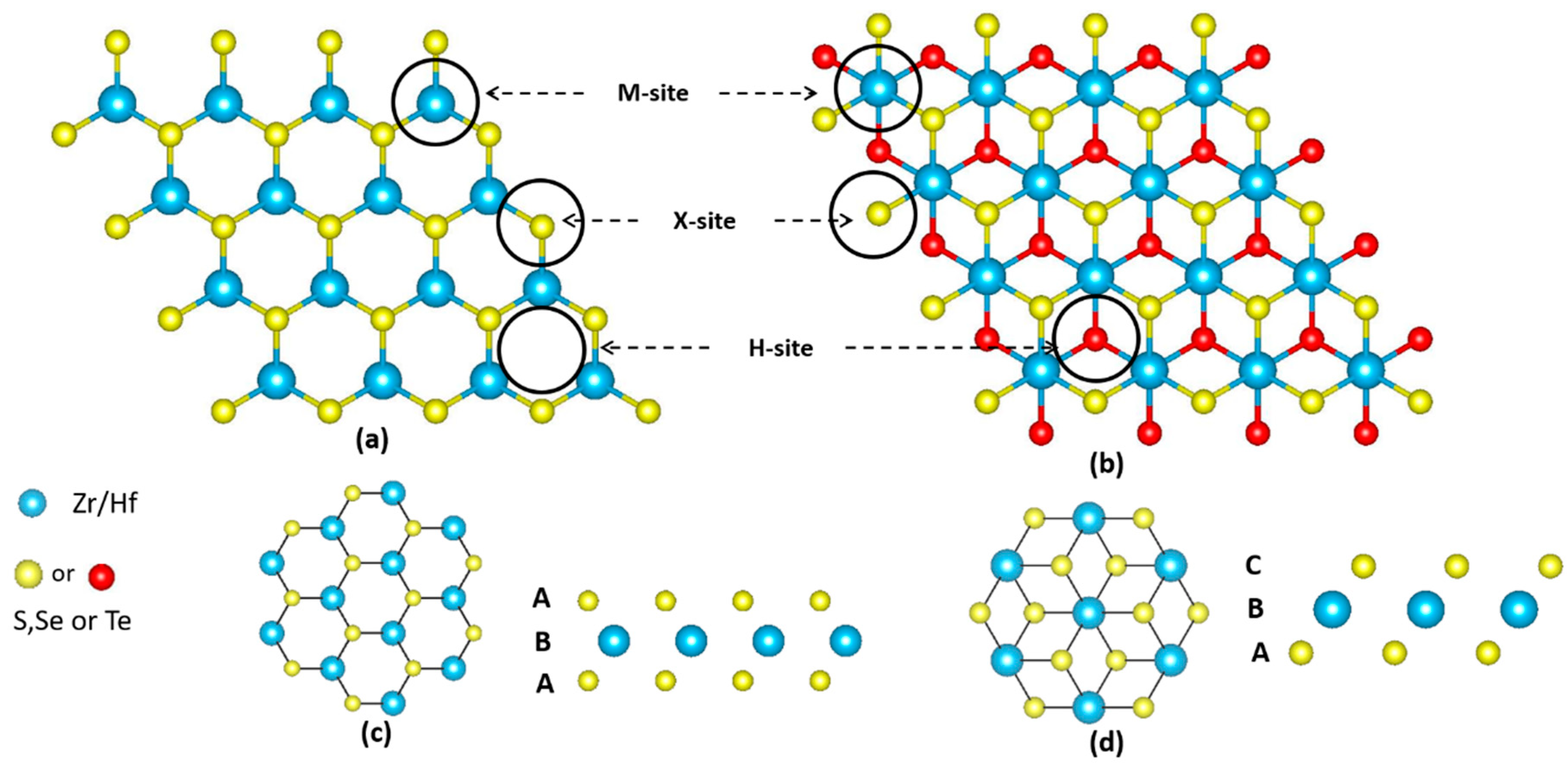
Prior to NH
3 (NO
2) adsorption, the lattice parameters (
a) of the 1T and 1H Zr (Hf) dichalcogenides were calculated. To the best of our knowledge, only the 1T structure has been taken into consideration. To date, no lattice parameter data, either theoretical or experimental, that are related to 1H Zr (Hf) dichalcogenides, were published and made available. Hence, in this work, the 1H structure lattice parameters are discussed by comparisons with the 1T structure.
Table 1 summarizes the optimized lattice parameters (Å) of the 2D 1T and 1H Zr (Hf) dichalcogenides. The lattice parameters of 1H are slightly smaller in all cases, as compared to the 1T Zr (Hf) dichalcogenides, which are associated with a decrease in the ionic radius of S. This is due to differences in atom stacking: 1H possess an ABA-type atomic staking, while 1T demonstrates an ABC-type atomic staking. As the atomic indices change from Te to Se and from Se to S, the lattice constants and metal-to-chalcogen bond lengths decrease due to the decreased atomic radius of the chalcogen. When switching from 1T to 1H phases, similar changes occur. The maximum difference in the calculated lattice parameters of the 1H and 1 T structure is found for HfS
2 (3.04%), whereas a minimum is found for ZrTe2 (0.77%); we find the overall order HfS
2 > ZrS
2 > HfSe
2 > ZrSe
2 > HfTe
2 > ZrTe
2. The calculated lattice parameters of the 1T-structured Zr (Hf) dichalcogenides are in close agreement with reported theoretical and experimental lattice parameters [
38,
39,
40,
41]. No experimental data are available for the lattice parameter of 1T-HfTe
2 and 1T-ZrTe
2. The variation of lattice parameters from previous theoretical data is due to the experimental conditions and the level of theory used for the calculations.
To investigate their electronic properties, we focused on the band structures of the 1T and 1H Zr (Hf) dichalcogenides and compared 1T relative to 1H in terms of their conduction bands, valance bands, and band gaps.
Figure 2 depicts the band structures of the pristine 2D 1T and 1H Zr (Hf) dichalcogenides obtained by the PBE method. The band structures show that they are indirect band gap semiconductors, similar to corresponding bulk TMDCs. This feature is different to that seen for some other TMDCs, such as MoS
2 or WS
2. The bulk MoS
2 and WS
2 systems show indirect bandgap transitions, but they gradually shift to direct transitions for the monolayer [
15]. Further, 1T-HfTe
2 and 1T-ZrTe
2 show semimetallic features instead of semiconductor features, which is consistent with earlier experimental [
42] and theoretical [
40,
43] reports.
Table 2 summarizes the calculated band gaps of the pristine 2D 1T and 1H Zr (Hf) dichalcogenides (S, Se & Te) [
39,
40,
41,
43,
44]. To date, no reports are available on the band structure and band gap of 1H Zr (Hf) dichalcogenides.
Researchers reported theoretically that in 1T-HfS
2, the Hf–d and S–p states are located between −5 eV and the Fermi energy (E
F) [
40], whereas, the bands from E
F to 2.4 eV (~ 3 eV for 1H-HfS
2) consist of Hf–d and Hf–f states with a small contribution from the S–p state [
40]. The valance band maximum (VBM) is observed at Γ, which is consistent with the calculations of Murray et al. [
45], Mattheis [
46], Fong et al. [
47], and Reshak and Auluck [
40]. The conduction band minimum (CBM) is located at M, in agreement with the calculations of Fong et al. [
47] and Traving et al. [
48]. Further, researchers reported theoretically that a strong hybridization exists between the Hf–f and Hf–d states below and above E
F, respectively, and a weak hybridization exists between the Hf–d and S–p states below E
F [
40]. Conversely, the 1H-HfS
2 band gap (1.15 eV) is slightly smaller than that of 1T-HfS
2 (1.28 eV). The conduction band slightly shifts to a lower value of 0.15 eV. Further, we find that the energy band structures pattern of 1H-HfS
2 is different to that of 1T-HfS
2.
The band structure of 1T-HfSe
2 is similar to that of 1T-HfS
2, but it exhibits a smaller energy gap (
Table 2). Replacing S with Se causes a separation of the Hf–f states from the Hf–d states below and above E
F [
40]. Further, the hybridization below E
F between Hf–d and Se–p is stronger than in 1T-HfS
2. Identical to 1T-HfS
2, the VBM is located at Γ, and the CBM is at M, in agreement with Murray et al. [
45]. Although, the band structures of 1H and 1T HfSe
2 differ from each other, the positions of the valance and conduction bands are identical, and hence both show nearly the same band gap value.
In 1T-ZrS
2, the VBM is located at Γ, while the CBM is located between Γ and K, resulting in an indirect gap of 1.13 eV. It is known theoretically that the band between −5 eV to E
F and E
F to 3 eV is composed of Zr-d and a small contribution from S-p states [
43], as well as a strong hybridization between Zr-d and S-p states below E
F [
43]. The 1T-ZrS
2 band looks similar to that of 1T-HfS
2 but with a slightly decreased bandgap. Conversely, the 1H-ZrS
2 bands not only match those of 1H-HfS
2, but they also show nearly the same electronic gap. However, the 1H-ZrS
2 band structure is quite different to that of 1T-ZrS
2, although they demonstrate nearly the same bandgap (
Table 2) with identical band positions.
In 1T-ZrSe
2, the VBM is located at Γ, and the CBM is at M [
43,
45]. With some minor differences, the band structure of 1T-ZrSe
2 is like that of 1T-ZrS
2, such as the reduction in the bandwidth of the Se-S group that is shifted toward lower energies with respect to E
F along with a second group band enhancement [
43]. Furthermore, the shift in the conduction bands at about 0.5 eV toward lower energies leads to 1T-ZrSe
2, demonstrating a smaller energy gap than 1T-ZrS
2. In contrast, no shifting and enhancement of second group band toward EF in 1H-ZrSe
2 than 1H-ZrS
2. Additionally, the conduction band in 1T-ZrS
2 shifts toward E
F less than that of 1T-ZrSe
2. Thus, 1H-ZrSe
2 possesses a higher band gap (0.85 eV) than 1T-ZrSe
2 (0.41 eV).
In 1T-ZrTe
2 (1T-HfTe
2), the occupied and unoccupied bands move toward E
F, which closes the energy gap and indicates metallic behavior. Also, a strong hybridization exists between the Te–p and Zr (Hf) d states below E
F [
40,
43]. Interestingly, 1H-ZrTe
2 (1H-HfTe
2) still shows semiconducting behavior, although its energy gap is lower than that of 1H-ZrSe
2 (1H-HfSe
2). A rise in the conduction band and fall in the valance band toward E
F is clearly observed.
It is to be noted that the Eg value of ZrS
2 (HfS
2) is a maximum, and it decreases as we replace chalcogen S with first Se and then Te. Although the amount of decrease in the Eg value in the Zr dichalcogenides differs to that of the Hf dichalcogenides, their decreasing trends are similar. The band structure of the Zr dichalcogenides looks similar to that of the Hf dichalcogenides, except for the case of 1H-ZrSe
2 and 1H-HfSe
2 (where they look different), even though their Eg values differ. Furthermore, both 1T-HfTe
2 and 1T-ZrTe
2 depict semimetallic natures. In the 1H structure, as S is replaced by Se, a large reduction occurs in the Eg value for the Hf-based TMDCs relative to the Zr-based TMDCs, while the situation is reversed for materials containing 1T structures. Also, it is well-known that 1T-ZrTe
2 (1T-HfTe
2) possesses a semimetallic nature. However, in the case of 1H structures, both materials show band openings; 1H phase Zr(Hf) dichalcogenides depict a band gap energy ranging from 0.29–1.15 eV, while in the 1T phase, the range is 0.41–1.29 eV. These moderate Eg values are comparable to other semiconductor materials such as Si (Eg = 1.14 eV), Ge (Eg = 0.67 eV), and PbS/Se/Te (Eg = 0.37/0.27/0.29 eV) [
49]. A semiconductor of this nature can lead to the use of these materials in different applications.
Thereafter, NH
3 and NO
2 adsorption on the trigonal prismatic (1H) and octahedral (1T) phases was carried out. First, we optimized the atomic geometries of the NH
3 and NO
2 gas molecules using the DFT approach. Based on our calculated results, the bond lengths of the NH bonds of the NH
3 molecule and the NO bonds of the NO
2 molecule are 1.02, and 1.21 Å, respectively. These are in reasonable agreement with previously reported data [
50,
51]. Moreover, the structure of the considered 4 × 4 × 1 supercell of Zr (Hf) dichalcogenides monolayer was geometrically optimized.
To search for the most stable configuration of the NH
3 (NO
2) molecules on the Zr (Hf) dichalcogenide monolayer, various adsorption positions were examined. For each adsorption configuration, an initial, reasonable distance between the gas molecules and the substrate was chosen.
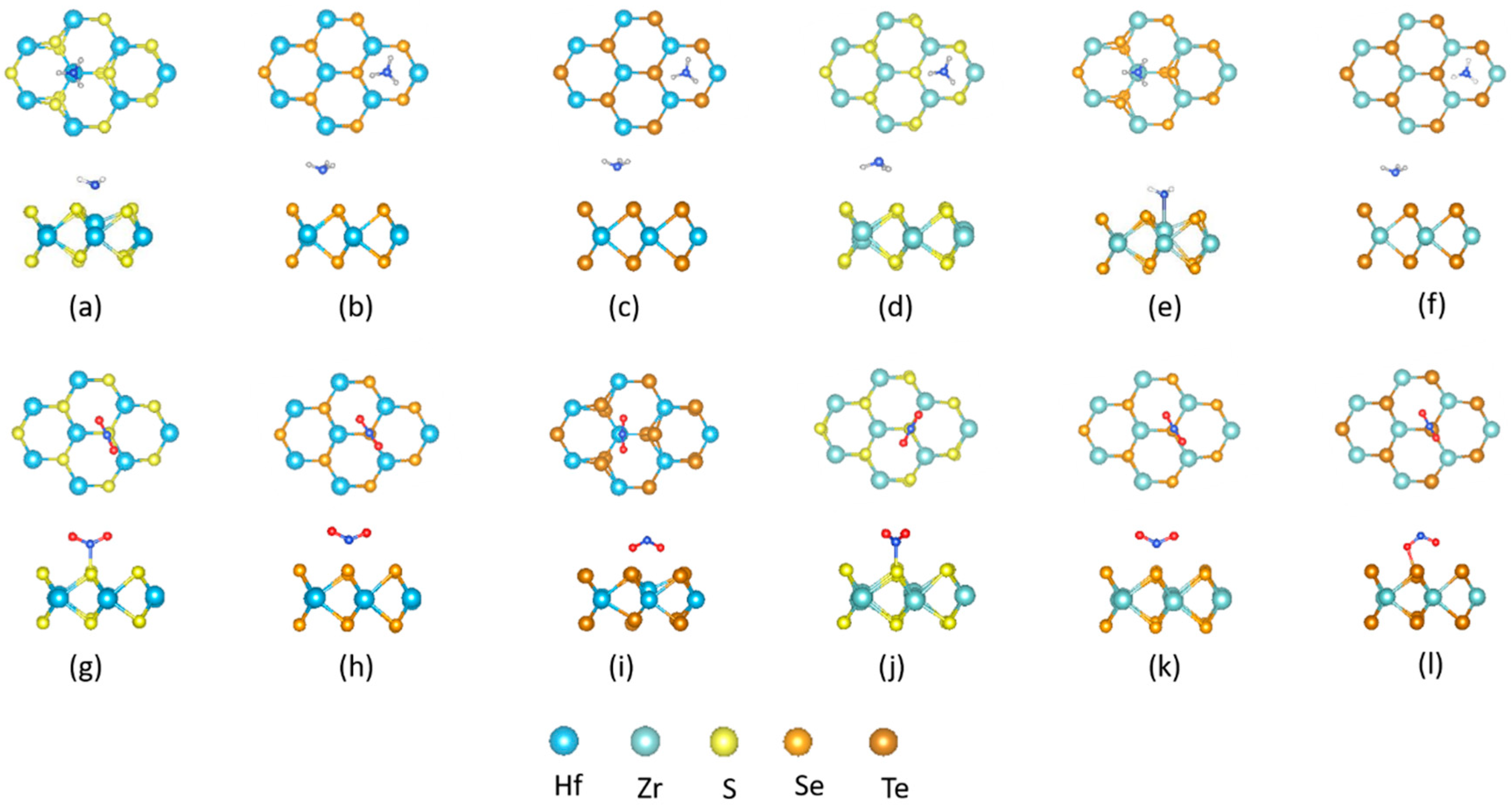
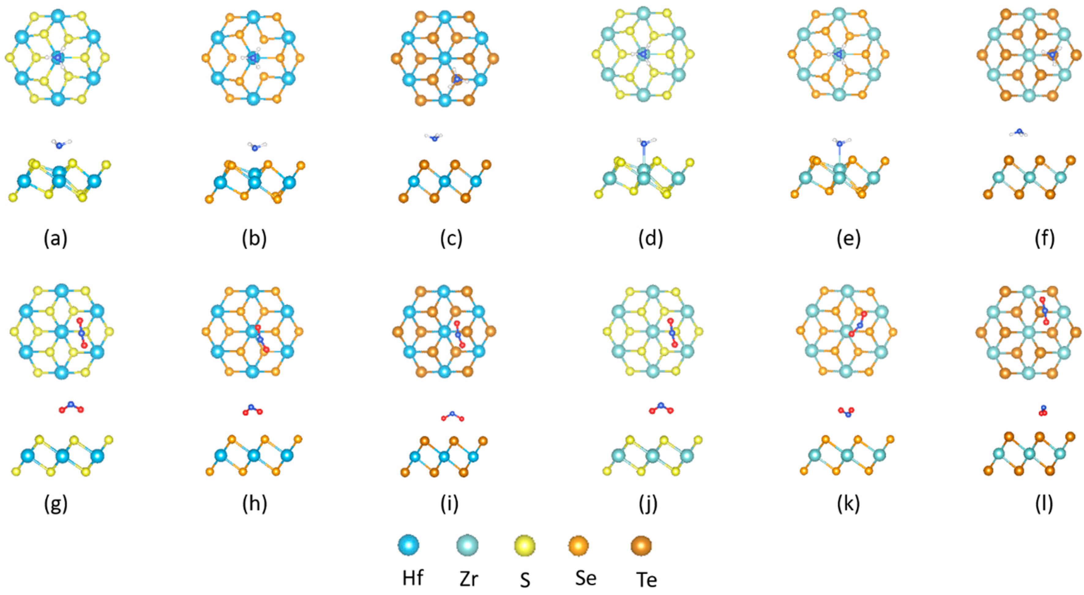
Figure 3 depicts the typical optimized geometry configurations of the NH
3- and NO
2-adsorbed 1H Zr (Hf) dichalcogenide monolayer. Configurations a–f represents the adsorption of NH
3 molecules on the 1H Zr (Hf) dichalcogenides, while configurations g–l shows the interaction between the NO
2 gas molecules and the 1H Zr (Hf) dichalcogenide monolayer. H-upward (U-orientation) is the preferable configuration for the NH
3 molecules, except for the case of 1H-ZrS
2, where H is oriented toward the adsorbing surface. Furthermore, the T
M-site is preferred for NH
3 adsorption on 1H-HfS
2 and 1H-ZrSe
2, where the adsorption-distances (d; i.e., the shortest atom-to-atom distance between the gas molecules and the substrate) are 2.43 and 2.49 Å (
Table 3), respectively, suggesting NH
3 adsorbs more strongly on 1H-HfS
2 than 1H-ZrSe
2. The remaining 1H Zr (Hf) dichalcogenides adsorb NH
3 on the T
H-sites with minimum adsorption-distances on HfSe
2 (3.38 Å). Interestingly, for all cases, no NH
3 adsorption takes place on the chalcogen sites. In contrast, NO
2 preferably adsorbs only on T
X-sites with D-orientation on HfTe
2 and ZrTe
2, with the same adsorption distance (2.28 Å). The U-oriented NO
2 adsorbs on the remaining 1H Zr (Hf) dichalcogenides, with a minimum adsorption-distance of 2.02 Å on 1H-HfS
2. Conversely, the NH
3 (NO
2) molecules adsorb differently on the 1T Zr (Hf) dichalcogenides.
The optimized geometric configurations of the molecularly adsorbed NH
3 and NO
2 on the 1T Zr (Hf) dichalcogenides monolayers are summarized in
Figure 4, where configurations a–f and g–l represents the adsorption of NH
3 and NO
2 molecules on the 1T Zr (Hf) dichalcogenides, respectively. As compared to 1H, the U-orientation is favorable for NH
3 on the 1T Zr (Hf) dichalcogenides except for 1T-ZrTe
2, where the D-orientation is favorable. The largest adsorption-distance is 3.87 Å (
Table 4) for NH
3 on the 1T Zr (Hf) dichalcogenides. The D-orientation (in 1H) changes to U-orientation for NH
3 on 1T-ZrS
2. Additionally, the T
M-site is preferred over the T
H-site, which is the opposite situation compared with what was observed for the 1H Zr (Hf) dichalcogenides. Consistent with 1H, HfS
2 shows a minimum NH
3 adsorption-distance (2.42 Å). A fresh, no preference adsorption takes place on the chalcogen sites. Conversely, the D-orientation is favorable for NO
2 on the 1T Zr (Hf) dichalcogenides, differing from the previous three cases, with a minimum adsorption-distance of 3.21 Å on 1T-ZrTe
2, which is almost 1 Å larger than that found for 1H-ZrTe
2. Furthermore, the T
M and T
X-sites are equally favorable. The details are given in
Table 4. It is distinctly seen that in all four cases, the D-orientation exhibits a larger adsorption distance than the corresponding U-orientation. The smallest adsorption-distance on metal sites is found for NH
3 on 1T-HfS
2 (2.42 Å) and 1T-ZrS
2(2.44 Å), which are larger than the sum of the covalent atomic radii of Hf-N (2.26 Å) and Zr-N (2.28 Å). Similarly, the smallest adsorption distance on the chalcogen is found for NO
2 on 1H-HfS
2 (2.02 Å), 1H-ZrSe2 (2.17 Å), and 1H-HfTe2(1H-ZrTe2) (2.28 Å), which are significantly larger than experimental average bond lengths of S-N (1.71 Å), Se-N (1.82 Å), and Te-N (2.02 Å) [
52]. Thus, no chemical bonds are expected to form, and only the physisorption of NH
3 and NO
2 takes place on the 1H and 1T Zr (Hf) dichalcogenides.
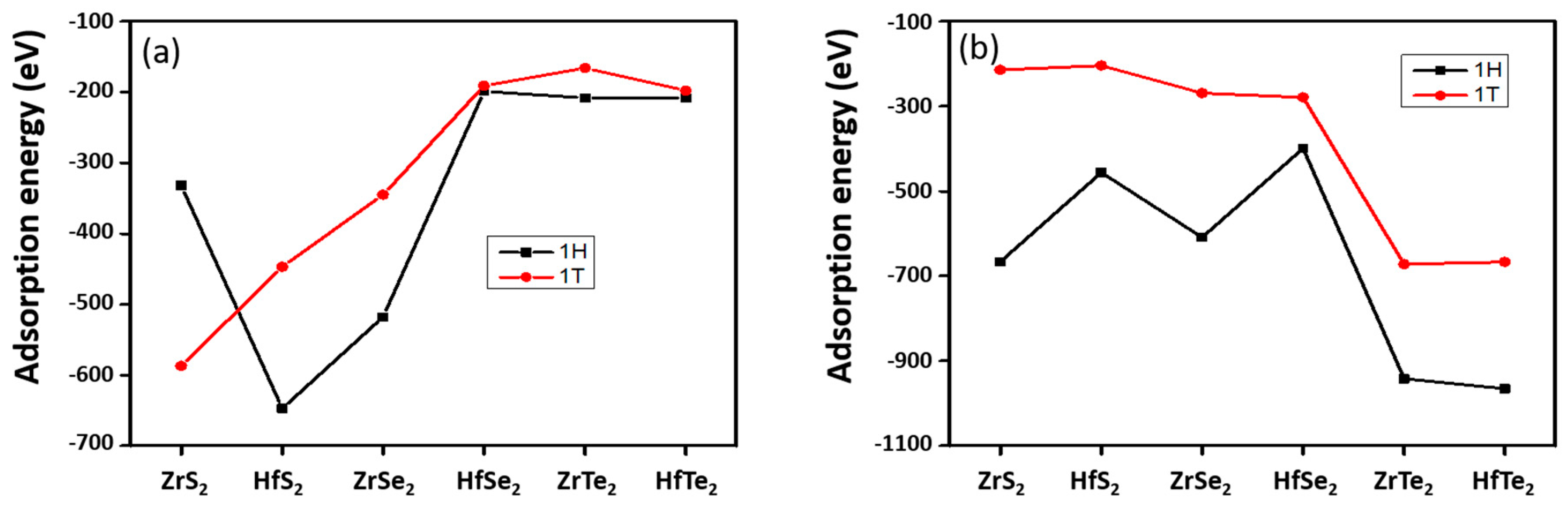
A negative adsorption energy implies that the adsorption of the NH
3 (NO
2) molecules on the 1H and 1T Zr (Hf) dichalcogenides is energetically favorable [
53]. The adsorption energy (E
ads) of NH
3 and NO
2 on the 1H and 1T Zr (Hf) dichalcogenides at different sites (H-site, T
M-site, T
X-site) was calculated and plotted, as shown in
Figure 5. In case of the 1H Zr (Hf) dichalcogenides, the largest calculated NH
3 adsorption energy is −647 meV on 1H-HfS
2, where adsorption took place on the T
M-sites, and the smallest is −199 meV on the 1H-HfSe
2 (T
H-site). Researchers observed that the metal sites are more energetically favorable than the T
H-sites, and no NH
3 adsorption occurs on the T
X-site. In addition, researchers observed that the U-orientation is preferred to the D-orientation on the T
M-sites. Furthermore, 1H-HfS
2, 1H-ZrS
2, and 1H-ZrSe
2 are more energetically favorable for NH
3 adsorption than 1H-HfSe
2, 1H-HfTe
2, and 1H-ZrTe
2. The order of favorability is HfS
2 > ZrSe
2 > ZrS
2 > HfTe
2 (ZrTe
2) > HfSe
2. Conversely, NO
2 adsorbs only on the T
X-sites of the 1H Zr (Hf) dichalcogenides. Compared to NH
3, NO
2 shows a high absorption favorability, as a more negative adsorption energy is observed on all surfaces (
Table 3). Instead of 1H-HfS
2, 1H-HfTe
2 shows high favorability to NO
2 adsorption. Interestingly, 1H-HfTe
2 and 1H-ZrTe
2 shows high NO
2 adsorption energies, in contrast to the energies of NH
3 adsorption. The order of NO
2 adsorption favorability is HfTe
2 > ZrTe
2 > ZrS
2 > ZrSe
2 > HfS
2 > HfSe
2. Although NO
2 shows high adsorption favorability relative to NH
3 on the 1H Zr (Hf) dichalcogenides, NH
3 is more favorable on 1H-HfS
2 than NO
2, which exhibits an adsorption energy almost 200 meV larger.
Table 4 depicts the calculated E
ads values for NH
3 and NO
2 on the 1T Zr (Hf) dichalcogenides. NH
3 shows an energetically high adsorption favorability on 1T-ZrS
2 surfaces, with an E
ads value of −587 meV (T
M-sites) and a lower value on 1T-ZrTe
2 (−166 meV, T
H-sites) (
Figure 5). The T
M-sites show higher NH
3 adsorption favorability than the T
H-sites, consistent with what was seen for NH
3 on the 1H Zr (Hf) dichalcogenides. The preferential adsorption site of NH
3 shifts from the T
H-sites to the T
M-sites for 1T-ZrS
2 and 1T-HfSe
2. The order of NH
3 adsorption favorability also changes, suggesting that the surfaces of the 1H and 1T Zr (Hf) dichalcogenides behave differently. Conversely, this behavior is consistent with the 1H surfaces of 1T-HfTe
2 and 1T-ZrTe
2, showing high NO
2 adsorption favorability. Also, instead of only T
X-sites, energetically favorable NO
2 adsorption on T
M-sites for 1T-HfSe
2, 1T-ZrSe
2, and 1T-HfTe
2 is observed. Thus, NH
3 adsorption is more energetically favorable than NO
2 on 1T-HfS
2, 1T-ZrS
2 and 1T-ZrSe
2, while the opposite situation exists for 1T-HfSe
2, 1T-HfTe
2, and 1T-ZrTe
2.
It is noteworthy that, consistently with all cases, the 1H-phase demonstrates different E
ads values with high adsorption favorability than the 1T-phase (
Figure 5). This situation is reversed for NH
3 on ZrS
2, where the 1T-phase is more favorable for adsorption than the 1H-phase. Conversely, the values of E
ads for HfSe
2 and HfTe
2 are almost the same in both phases.
Next, a Bader analysis was employed to estimate the charge (ΔQ) transfer from the NH
3 (NO
2) to the surface of the 1T-(1H-) Zr (Hf) dichalcogenides (or vice versa), where the change is either positive or negative. The charge transfer from the molecules to the dichalcogenide’s surface is defined as positive here, whereas from the surface to the molecules is negative. Researchers noticed that, in order for a charge transfer to occur, the property of the material, the adsorption sites on the dichalcogenide’s surface, and the orientation of the gas molecules are crucial factors [
54].
Researchers found that the NH
3 that adsorbs on the 1H Zr (Hf) dichalcogenides depicts a positive charge, suggesting NH
3 acts as a charge-donor (
Table 3), which is well known experimentally. Although NH
3 strongly adsorbs on 1H-HfS
2 (M-sites), the maximum charge transfer (0.152 e) takes place when NH
3 adsorbs on 1H-ZrS
2 (H-sites). Interestingly, the adsorption distance is a maximum in this case. The fact that NH
3 donates more charges at M-sites than at H-sites on MoS
2 is noteworthy [
35]. The charges transferred to 1H-HfSe
2, 1H-ZrSe
2, 1H-HfTe
2, and 1H-ZrTe
2 are 0.045, 0.081, 0.033, and 0.009 e, respectively. Comparatively more charge transfer occurs on the Zr-based chalcogenides compared to the Hf-based chalcogenides when adsorbed on the M-sites, while the opposite situation is seen on the H-sites. It seems to be that D-oriented NH
3 donates more charge than the U-oriented NH
3. Conversely, NO
2 accepts an electron from the 1H-Zr (Hf) dichalcogenides (
Table 3). This behavior is expected as NO
2 is a well-known charge acceptor [
35]. Like NH
3, NO
2 also depicts a high charge transfer on 1H-ZrTe
2 (0.622 e), where even 1H-HfTe
2 demonstrates a high NO
2 adsorption energy. Furthermore, higher charge transfers occur on the Zr-based chalcogenides than on the Hf-based chalcogenides, when adsorption occurs on the X-sites, considering the same chalcogen. Also, the D-oriented NO
2 accepts more charge than the U-oriented NO
2, except for the case of 1H-ZrSe
2.
Consistent with what was observed for the 1H surfaces, the NH
3 adsorbed by the 1T Zr (Hf) dichalcogenides also depicts a positive charge, implying that NH
3 is a donor (
Table 4). Comparatively, charge transfer enhances for the 1H-Zr (Hf) dichalcogenides, except for 1T-ZrS
2 and 1T-ZrSe
2, where it decreases. Interestingly, more charge transfer occurs on the Hf-based chalcogenides compared to on the Zr-based chalcogenides, due to the NH
3 adsorption taking place on either H-sites or M-sites, considering the same chalcogen. Also, the D-orientation shows a minimum charge transfer of 0.018 e on 1T-ZrTe
2, and it depicts a maximum for 1H-ZrS
2. The maximum charge transfer occurs for NH
3 adsorption on 1T-HfS
2, while it is a minimum on 1H-HfS
2, suggesting NH
3 behaves differently on 1T surfaces than 1H surfaces. Conversely, NO
2 accepts a maximum charge on 1T-ZrTe
2, similar to 1H-ZrTe
2. Furthermore, charge transfer is different on the 1T and 1H surfaces. Overall, NH
3 donates charges in the range of 0.01–0.15 e on 1H and 0.02–0.2 e on the 1T Zr(Hf) dichalcogenides. In contrast, NO
2 accepts charge in the interval of 0.18–0.62 e on 1H and 0.05–0.62 e on the 1T Zr(Hf) dichalcogenides.
Figure 6 depicts the correlation between E
ads and ΔQ for NH
3 (NO
2) on the Zr (Hf) dichalcogenides. The NH
3 (NO
2) molecules on the Zr (Hf) dichalcogenides depict a direct correlation between E
ads and ΔQ, where a low E
ads results in a low ΔQ, and vice versa. However, a different trend is seen for NH
3 on 1H-HfS
2 and 1H-ZrS
2. Interestingly, the value of E
ads for NH
3 on 1H-ZrS
2 is lower than that on 1H-HfS
2 and 1H-ZrSe
2. However, further charge transfer occurs in the case of NH
3 on 1H-ZrS
2. Similarly, NH
3 on 1T-ZrS
2 depicts a high E
ads, but more charge transfer occurs for NH
3 on 1T-HfS
2. In the case of NO
2 adsorption, only HfTe
2 depicts a contrary behavior. The charge transfers are quite low with respect to E
ads, as compared with the remaining Zr (Hf) dichalcogenides.
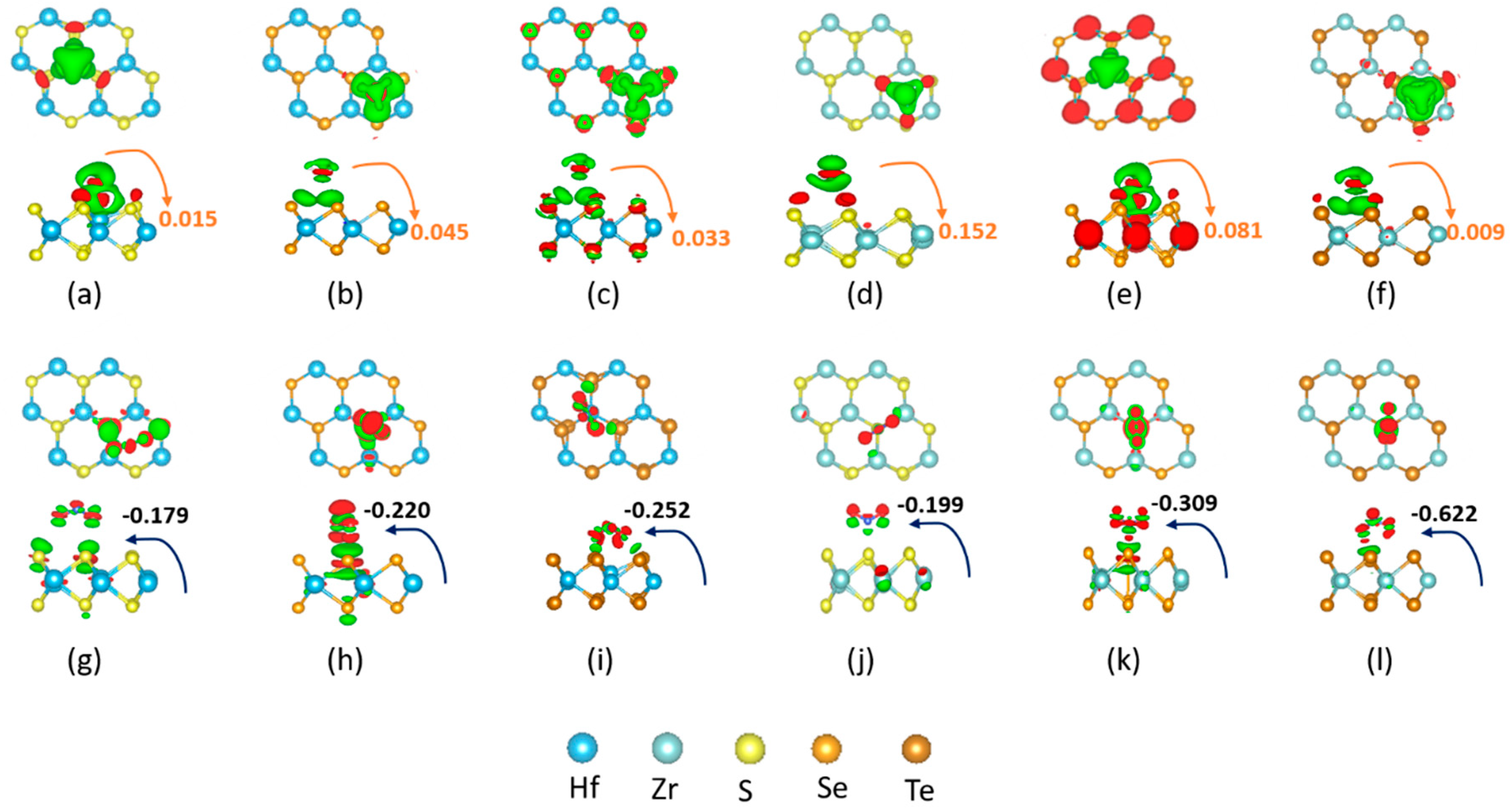
To gain further insight into the NH
3(NO
2)–TMDC interaction, we investigated the charge-transfer mechanism between them.
Figure 7 and
Figure 8 depict charge density difference images for NH
3 and NO
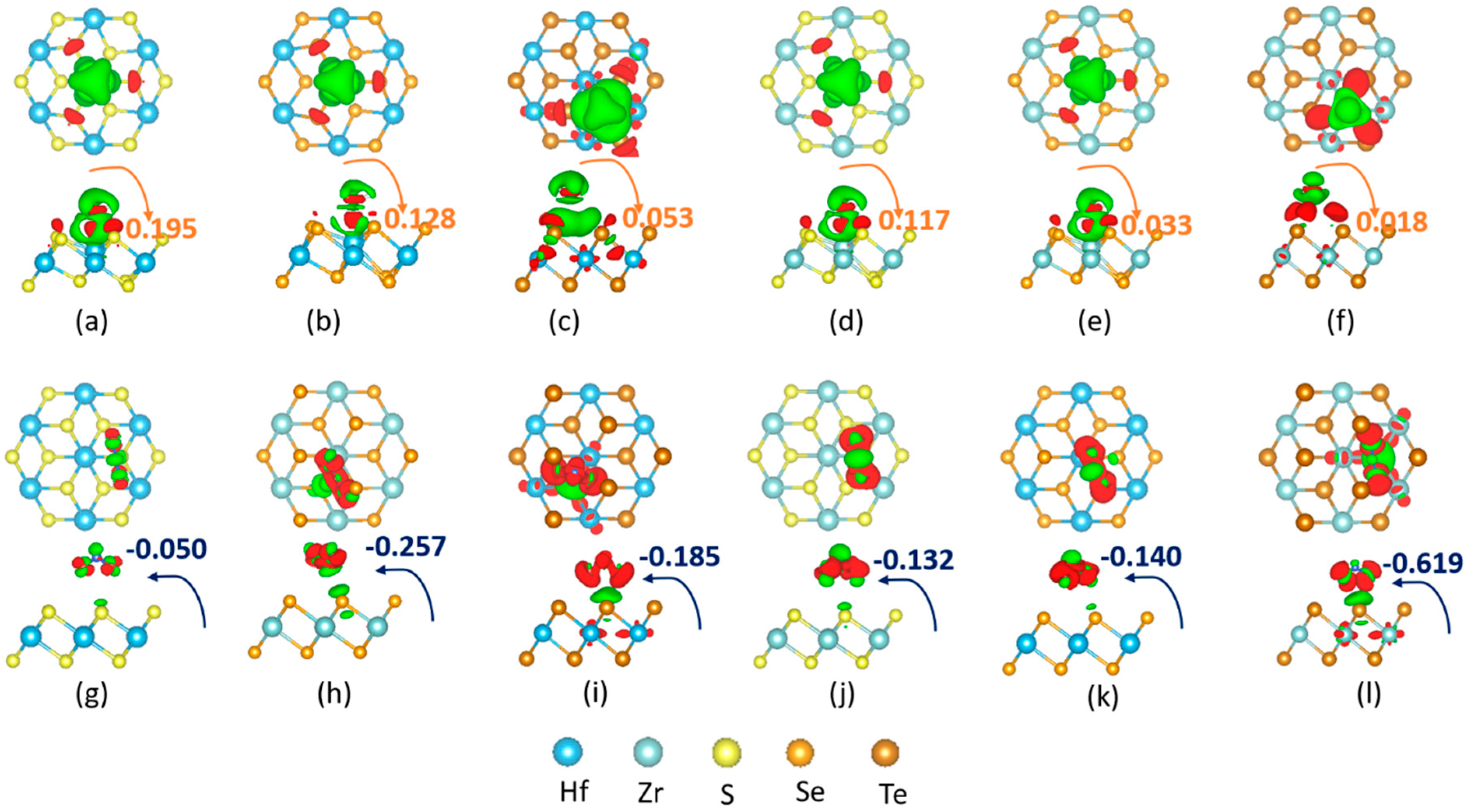
2 adsorbed on the 1H- (1T-) Zr (Hf) dichalcogenides. The red region shows the charge accumulation, while the green region represents the charge depletion. Different TMDCs polarize differently upon adsorption of NH
3 (NO
2), and the 1H surfaces show different polarizations than the 1T surfaces. Additionally, electrostatic interactions play a role in the attractive interaction. Researchers clearly observed that a charge accumulation occurs due to the adsorption of NH
3 on either of the 1H (
Figure 7) or 1T (
Figure 8) surfaces, suggesting NH
3 acts as a donor. Nevertheless, the NO
2 adsorption shows the opposite behavior. On the 1H surfaces, NH
3 adsorption shows a moderate charge density difference on 1H-HfS
2 and 1H-ZrSe
2, giving rise to a moderate interaction energy and a comparatively low charge density difference on the remaining surfaces. This explains why the former exhibits larger adsorption energies (−647 and −518 meV for NH
3 on 1H-HfS
2 and 1H-ZrSe
2) than the latter (−199, −208, −332, and −208 meV for NH
3 on 1H-HfSe
2, 1H-HfTe
2, 1H-ZrS
2, and 1H-ZrTe
2) (
Table 3 and
Figure 6). In contrast, the polarization increases when NO
2, instead of NH
3, adsorbs on the 1H surfaces. Along with moderate, a comparatively strong polarization is observed on 1H-HfTe
2 and 1H-ZrTe
2. Conversely, instead of 1T-ZrSe
2, 1T-ZrS
2 shows a moderate polarization upon adsorption of NH
3. The remaining surfaces depict different polarizations compared to the corresponding 1H-surfaces; i.e., the NO
2 that adsorbed on the 1T surfaces shows less polarization for all cases.
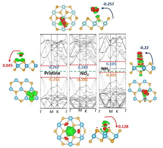
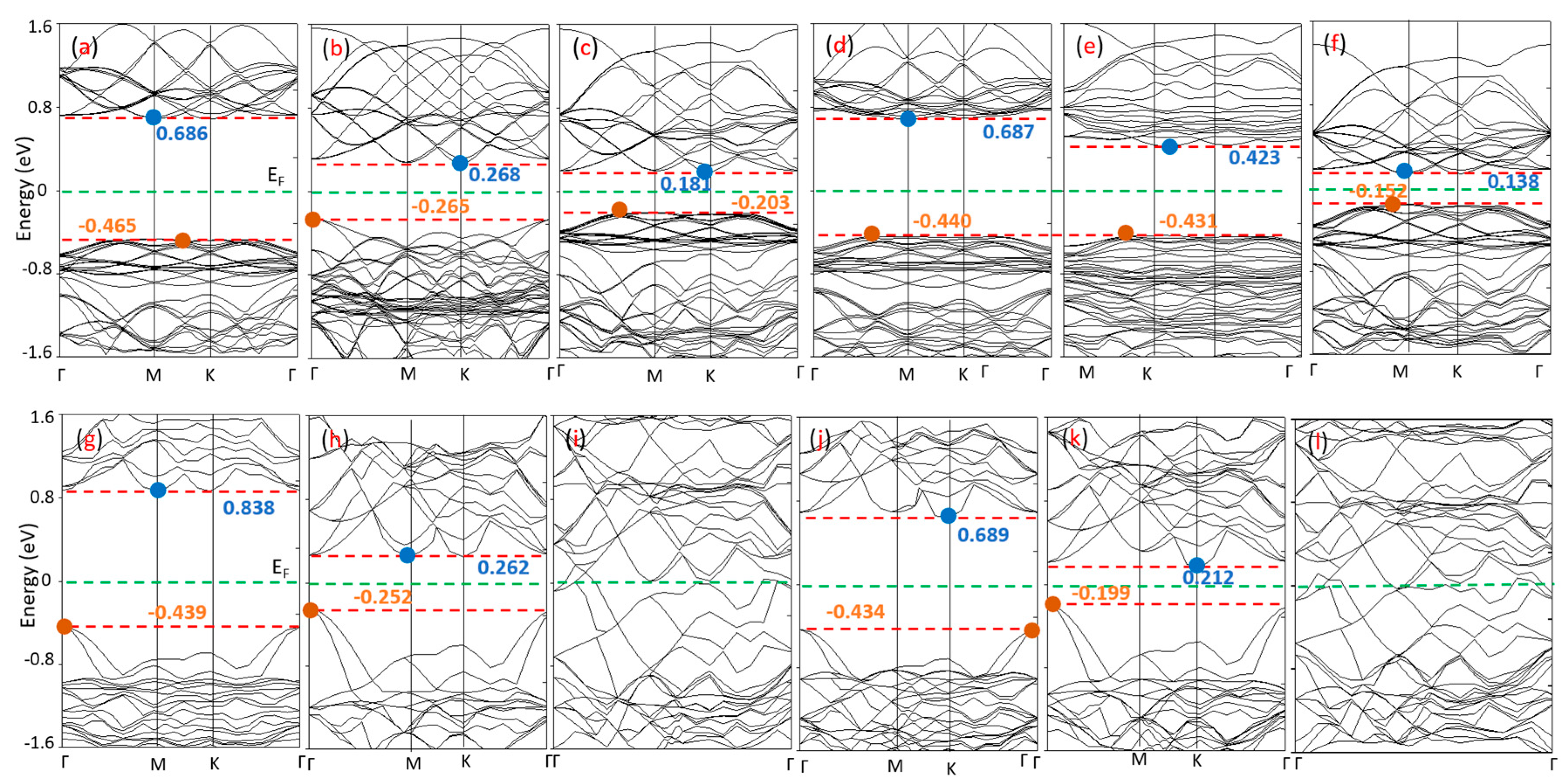
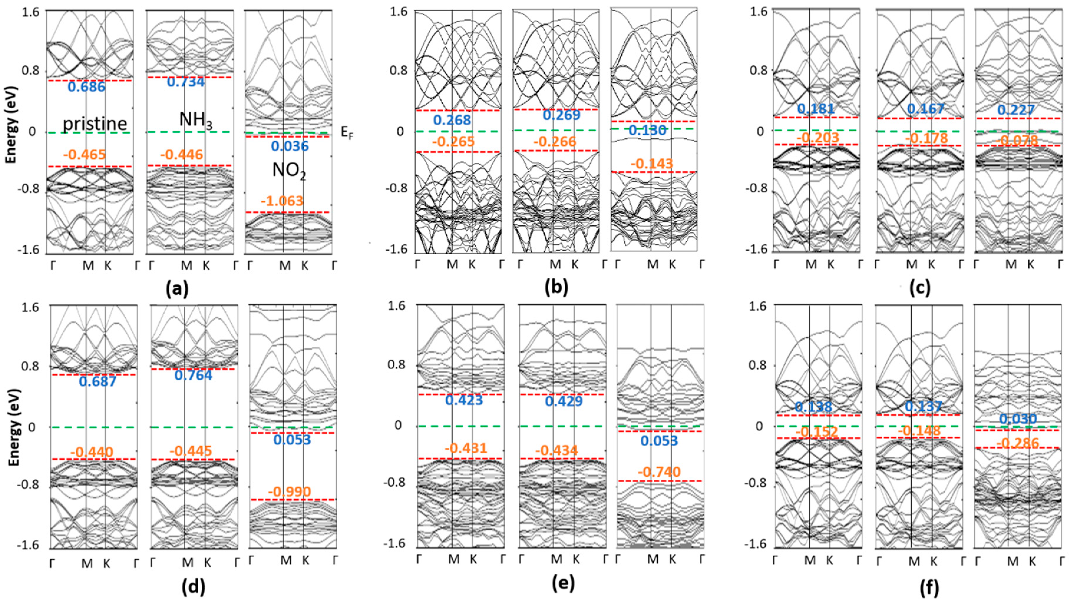
The electronic properties of NH
3 (NO
2) adsorbed on the 2D TMDCs were examined. Here, the position of the valance and conduction bands, and the change of the Fermi level, along with the pristine 1H (1T) band positions, were considered. The calculated band structure of NH
3 (NO
2) adsorbed on the 1H and 1T 2D Zr (Hf) dichalcogenides are plotted in
Figure 9 and
Figure 10, respectively. Researchers found that the valance band maxima and conduction band minima are not at the same points for all cases, implying they are all indirect band gap materials. Researchers observed that the adsorption of NH
3 molecules does not introduce any additional states within the band gap of the pristine 1H (1T) Zr (Hf) dichalcogenides. Furthermore, 0.001–0.04 eV changes were seen at the positions of the conduction and valance bands for most materials, which are almost insignificant and consistent with the adsorption of NH
3 on other metal chalcogenides [
35]. The conduction bands of 1H-HfS
2, 1H-ZrS
2, and 1T-ZrS
2 depict an upshift of 0.048, 0.077, and 0.043 eV, respectively, from the Fermi level. All the NH
3-adsorbed material bands features are similar to those of the pristine materials, except for 1H-HfS
2, 1T-HTe
2, and 1T-ZrTe
2, and an observable conduction band degeneracy is seen for 1H-HfS
2. Interestingly, gapless 1T-HTe
2 and 1T-ZrTe
2 depict band openings (~0.1 eV) with clearly separated conduction and valance bands after NH
3 adsorption, although the band gap values are very small.
Conversely, no influence of NO
2 adsorption on the band structures of 1T-HTe
2 and 1T-ZrTe
2 is seen. NO
2 adsorption induces a state within the band gap of Zr (Hf) dichalcogenides, contrary to that happens after NH
3 adsorption. In 1H-HfS
2 (1H-ZrS
2), NO
2 induces a state that crosses the Fermi level. Other state levels appear just above E
F. The states and conduction bands are so near (
Figure 9) that the electron can easily move to-and-fro. Therefore, the estimated bandgaps of 1H-HfS
2 and 1H-ZrS
2 are less than those of the pristine ones. In 1H-HfSe
2, a single state at −0.1 eV in-between the bandgap is observed with a slight downshifting of the conduction band (0.122 eV), and a comparatively large valance band shift (0.138 eV) results in bandgap enhancement. 1H-ZrSe
2 depicts features similar to those seen for 1H-ZrS
2; however, no conduction band expansion occurs. Two additional states cut the E
F, where one appears below E
F in the case of 1H-HfTe
2. No significant shifting in the bands occurs. Like 1H-ZrS
2 and 1H-ZrSe
2, the 1H-ZrTe
2 band is just above the Fermi level, with conduction bands near to these levels, while two states cut E
F in 1H-HfTe
2, and one appears just below E
F. These states are near to the valance band. Easy to-and-fro movement of the electrons from these states to the conduction band is observed for NH
3 adsorbed on the 1H Zr (Hf) dichalcogenides, except 1H-HfSe
2 and 1H-HfTe
2, where electron transfer occurs from the valance band. The NO
2-adsorbed 1T Zr(Hf) dichalcogenides bands are identical to those of the pristine materials, but with additional band states. A single state between E
F and the conduction band appears in the NO
2-adsorbed 1T-HfS
2, while the band positions remain unchanged. Similar phenomena is observed for 1H-HfSe
2, but with an upward shift in the band positions. Furthermore, a single state appears just below the conduction band in the NO
2-adsorbed 1T-ZrS
2, where a minor upward shift in the valance band results in a decrease in the band gap. The bands of 1T-ZrS
2 shift like those of 1H-HfSe
2, where the two states cut E
F.


