Improved Field Electron Emission Properties of Phosphorus and Nitrogen Co-Doped Nanocrystalline Diamond Films

 ,
,  ,
,
Abstract
:
1. Introduction
2. Materials and Methods
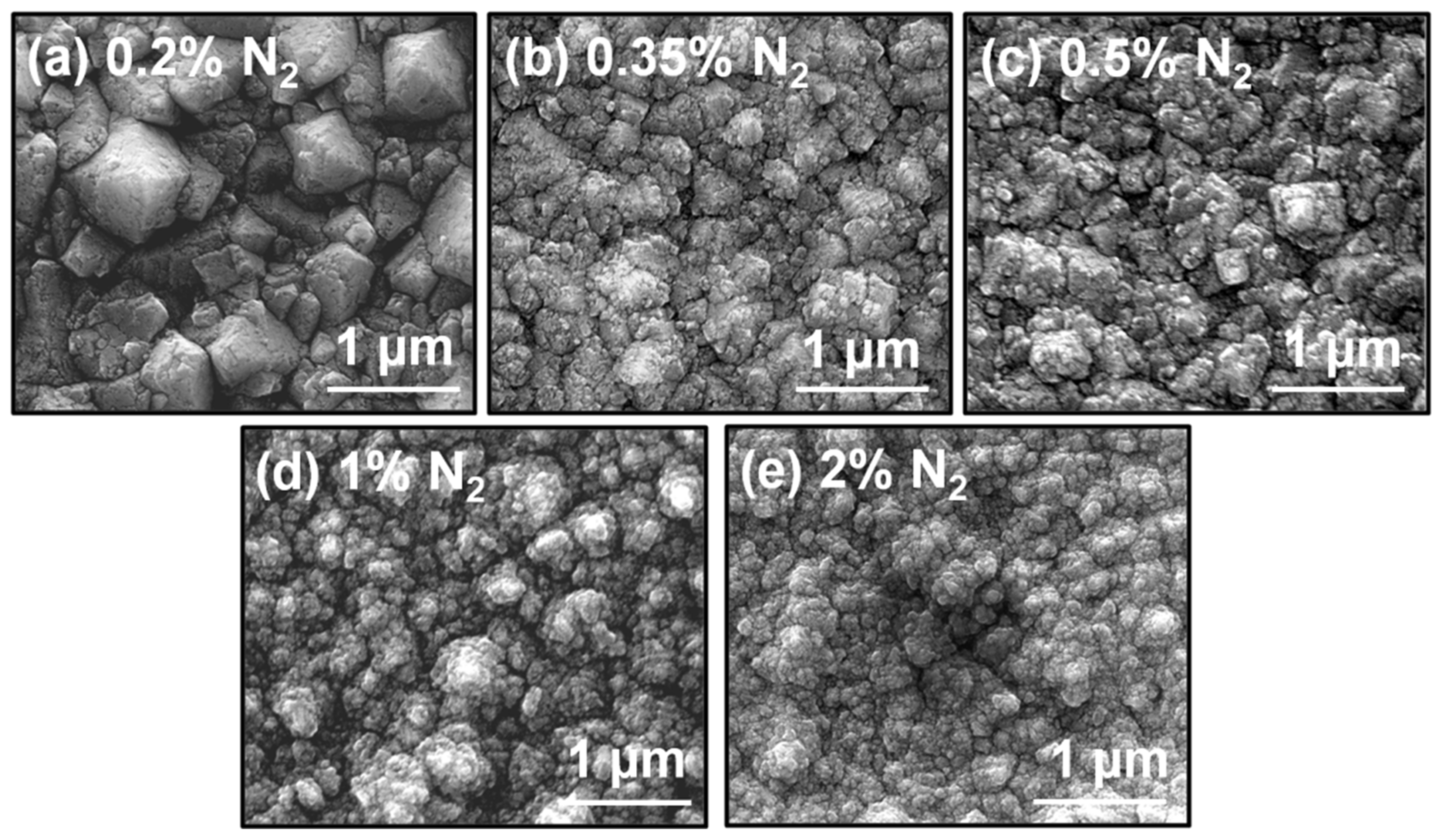
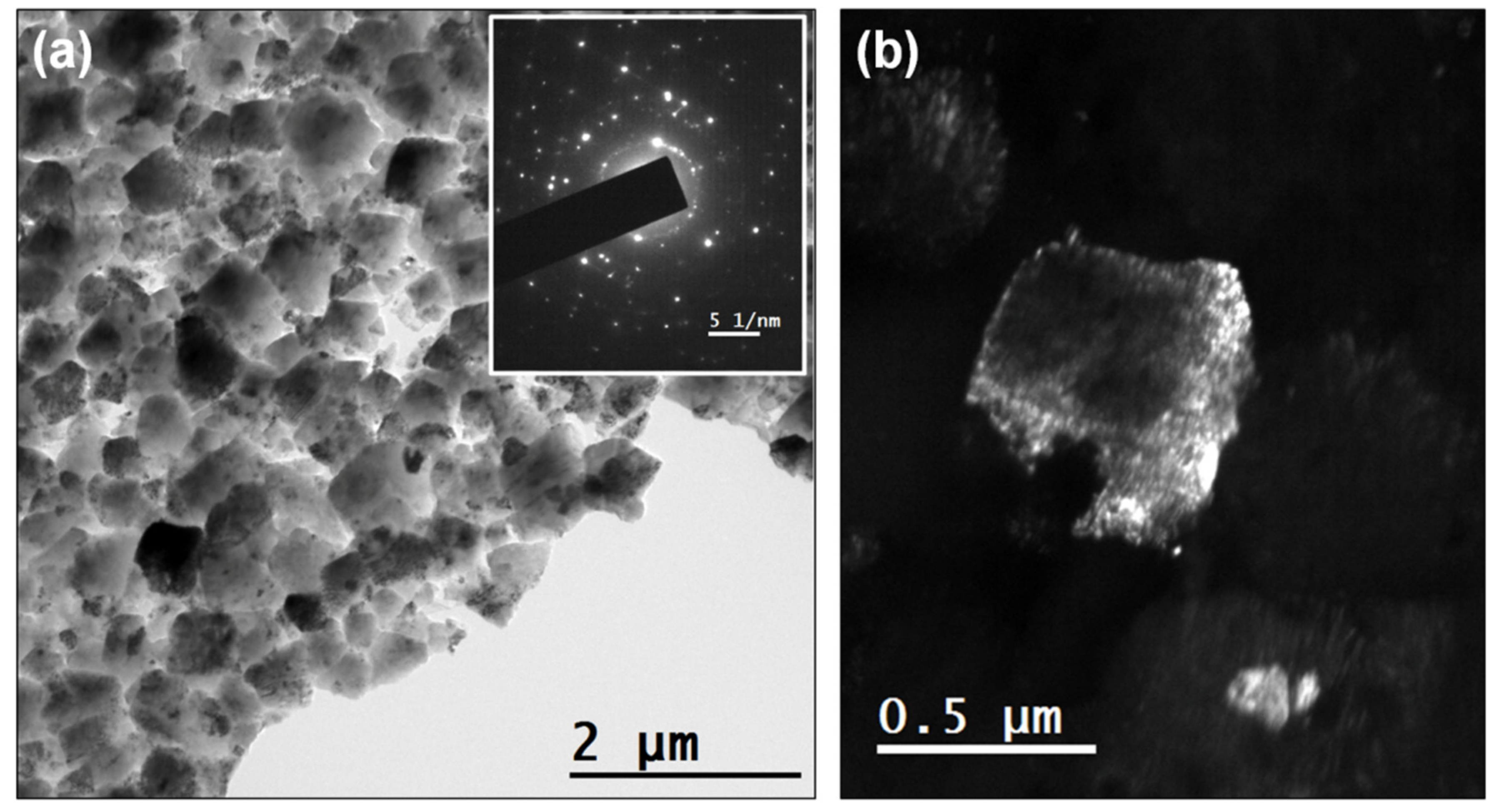
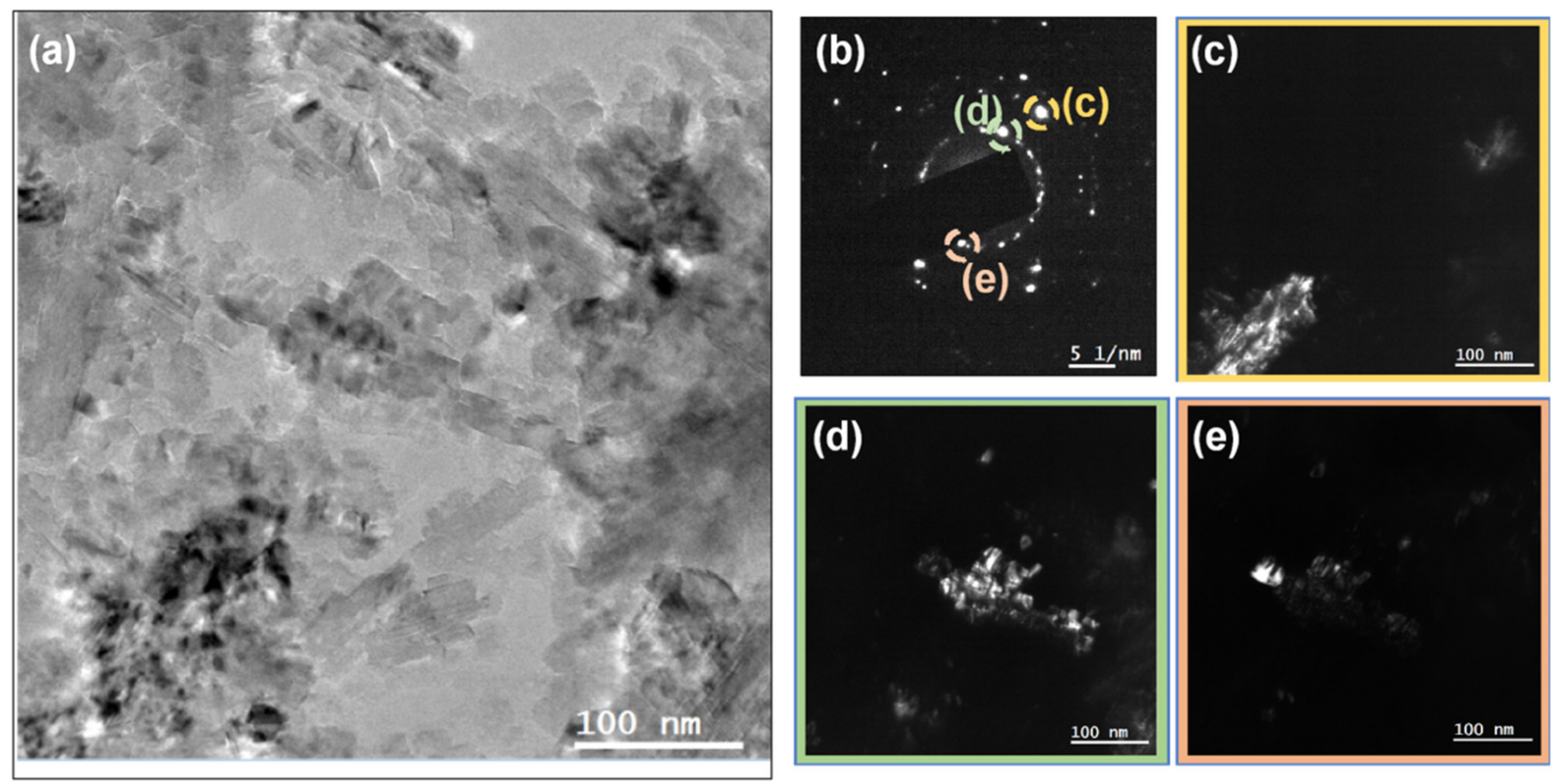
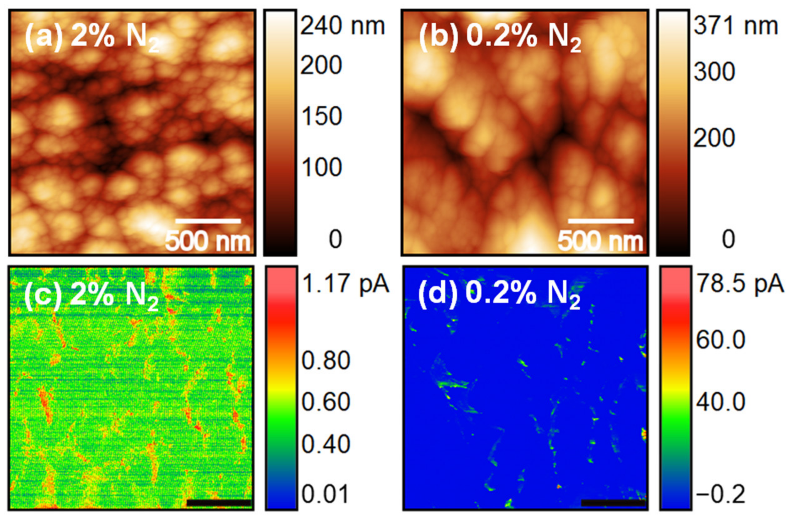
3. Results and Discussion
4. Conclusions
Author Contributions
Funding
Conflicts of Interest
References
- Balmer, R.S.; Brandon, J.R.; Clewes, S.L.; Dhillon, H.K.; Dodson, J.M.; Friel, I.; Inglis, P.N.; Madgwick, T.D.; Markham, M.L.; Mollart, T.P.; et al. Chemical vapour deposition synthetic diamond: Materials, technology and applications. J. Phys. Condens. Matter. 2009, 21, 364221. [Google Scholar]
- Sankaran, K.J.; Srinivasu, K.; Leou, K.C.; Tai, N.H.; Lin, I.N. High stability electron field emitters made of nanocrystalline diamond coated carbon nanotubes. Appl. Phys. Lett. 2013, 103, 251601. [Google Scholar]
- Terranova, M.L.; Orlanducci, S.; Rossi, M.; Tamburri, E. Nanodiamonds for field emission: State of the art. Nanoscale 2015, 7, 5094–5114. [Google Scholar]
- Sankaran, K.J.; Joseph, P.T.; Chen, H.C.; Tai, N.H.; Lin, I.N. Investigation in the role of hydrogen on the properties of diamond films grown using Ar/H2/CH4 microwave plasma. Diam. Relat. Mater. 2011, 20, 232. [Google Scholar]
- Arenal, R.; Bruno, P.; Miller, D.J.; Bleuel, M.; Lal, J.; Gruen, D.M. Diamond nanowires and the insulator-metal transition in ultrananocrystalline diamond films. Phys. Rev. B 2007, 75, 195431. [Google Scholar]
- Cuenca, J.A.; Sankaran, K.J.; Pobedinskas, P.; Panda, K.; Lin, I.N.; Porch, A.; Haenen, K.; Williams, O.A. Microwave cavity perturbation of nitrogen doped nano-crystalline diamond films. Carbon 2019, 145, 740. [Google Scholar]
- Bhattacharyya, S.; Auciello, O.; Birrell, J.; Carlisle, J.A.; Curtiss, L.A.; Goyette, A.N.; Gruen, D.M.; Krauss, A.R.; Schlueter, J.; Sumant, A.; et al. Synthesis ad characterization of highly-conducting nitrogen doped ultrananocrystalline diamond films. Appl. Phys. Lett. 2001, 79, 1441. [Google Scholar]
- Sankaran, K.J.; Tai, N.H.; Lin, I.N. Microstructural evolution of diamond films from CH4/H2/N2 plasma and their enhanced electrical properties. J. Appl. Phys. 2015, 117, 075303. [Google Scholar]
- Pradhan, D.; Lin, I.N. Grain-size-dependent diamond-nondiamond composite films: Characterization and field-emission properties. ACS Appl. Mater. Interfaces 2009, 1, 1444–1450. [Google Scholar]
- Sankaran, K.J.; Yeh, C.J.; Hsieh, P.Y.; Pobedinskas, P.; Kunuku, S.; Leou, K.C.; Tai, N.H.; Lin, I.N.; Haenen, K. Origin of conductive nanocrystalline diamond nanoneedles for optoelectronic applications. ACS Appl. Mater. Interfaces 2019, 11, 25388–25398. [Google Scholar]
- Janssen, W.; Turner, S.; Sakr, G.; Jomard, F.; Barjon, J.; Degutis, G.; Lu, Y.G.; D’Haen, J.; Hardy, A.; Van Bael, M.; et al. Substitutional phosphorus incorporation in nanocrystalline CVD diamond thin films. Phys. Status Solidi RRL 2014, 8, 705–709. [Google Scholar]
- Haenen, K.; Lazea, A.; Barjon, J.; D’Haen, J.; Habka, N.; Teraji, T.; Koizumi, S.; Mortet, V. P-doped diamond grown on (110)-textured microcrystalline diamond: Growth, characterisation and devices. J. Phys. Condens. Matter 2009, 21, 364204. [Google Scholar]
- Williams, O.A.; Douheret, O.; Daenen, M.; Haenen, K.; Osawa, E.; Takahashi, M. Enhanced diamond nucleation on monodispersed nanocrystalline diamond. Chem. Phys. Lett. 2007, 445, 255. [Google Scholar]
- Wu, Z.S.; Pei, S.; Ren, W.; Tang, D.; Gao, L.; Liu, B.; Li, F.; Cheng, H.M. Field emission of single-layer graphene films prepared by electrophoretic deposition. Adv. Mater. 2009, 21, 1756. [Google Scholar]
- Birrell, J.; Gerbi, J.E.; Auciello, O.; Gibson, J.M.; Johnson, J.; Carlisle, J.A. Interpretation of the Raman spectra of ultrananocrystalline diamond. Diam. Relat. Mater. 2005, 14, 86. [Google Scholar]
- Xiao, X.; Birrell, J.; Gerbi, J.E.; Auciello, O.; Carlisle, J.A. Low temperature growth of ultrananocrystalline diamond. J. Appl. Phys. 2004, 96, 2232. [Google Scholar]
- Liu, J.; Zhirnov, V.V.; Myers, A.F.; Wojak, G.J.; Choi, W.B.; Hren, J.J.; Wolter, S.D.; McClure, M.T.; Stoner, B.R.; Glass, J.T. Field emission characteristics of diamond coated silicon field emitters. J. Vac. Sci. Technol. B 1995, 13, 422–426. [Google Scholar]
- Harniman, R.L.; Fox, O.J.; Janssen, W.; Drijkoningen, S.; Haenen, K.; May, P.W. Direct observation of electron emission from grain boundaries in CVD diamond by PeakForce-controlled tunnelling atomic force microscopy. Carbon 2015, 94, 386–395. [Google Scholar]
- Deshmukh, S.; Sankaran, K.J.; Srinivasu, K.; Korneychuk, S.; Banerjee, D.; Barman, A.; Bhattacharya, G.; Phase, D.M.; Gupta, M.; Verbeeck, J.; et al. Local probing of the enhanced field electron emission of vertically aligned nitrogen-doped diamond nanorods and their plasma illumination properties. Diam. Relat. Mater. 2018, 83, 118–125. [Google Scholar]
- Marcus, B.; Mermoux, M.; Vinet, F.; Campargue, A.; Chenevier, M. Relationship between emission spectroscopy and structural properties of diamond films synthesized by plasma-assisted chemical vapor deposition. Surf. Coat. Technol. 1991, 47, 608–617. [Google Scholar]
- Shigesato, Y.; Boekenhauer, R.E.; Sheldon, B.W. Emission spectroscopy during direct-current-biased, microwave-plasma chemical vapor deposition of diamond. Appl. Phys. Lett. 1993, 63, 314–316. [Google Scholar]
- Balestrino, G.; Marinelli, M.; Milani, E.; Paoletti, A.; Paroli, P.; Pinter, I.; Tebano, A. Systematic investigation of plasma emission spectra during microwave diamond deposition from CH4-CO2 and C2H2-CO2 gas mixtures. Diam. Relat. Mater. 1993, 2, 389–392. [Google Scholar]
- May, P.W.; Mankelevich, Y.A. From ultrananocrystalline diamond to single crystal diamond growth in hot filament and microwave plasma-enhanced cvd reactors: A unified model for growth rates and grain sizes. J. Phys. Chem. C 2008, 112, 12432–12441. [Google Scholar]
- Vandevelde, T.; Wu, T.D.; Quaeyhaegens, C.; Vlekken, J.; D’Olieslaeger, M.; Stals, L. Correlation between the OES plasma composition and the diamond properties during microwave PA-CVD with nitrogen addition. Thin Solid Films 1999, 340, 159–163. [Google Scholar]
- Eckert, M.; Neyts, E.; Bogaerts, A. Differences between ultrananocrystalline and nanocrystalline diamond growth: Theoretical investigation of CxHy species at diamond step Edges. Crys. Growth Des. 2010, 10, 4123–4134. [Google Scholar]
- Sankaran, K.J.; Kurian, J.; Chen, H.C.; Dong, C.L.; Lee, C.Y.; Tai, N.H.; Lin, I.N. Origin of a needle-like granular structure for ultrananocrystalline diamond films frown in a N2/CH4 plasma. J. Phys. D Appl. Phys. 2012, 45, 365303. [Google Scholar]


| Power | Pressure | Temperature | CH4 | PH3 | N2 | Ra | FWHM “dia” |
|---|---|---|---|---|---|---|---|
| 2100 W | 70 Torr | 760–800 °C | 1% | 250 sccm | 0.2% | 67 nm | 14.0 cm−1 |
| 2100 W | 70 Torr | 760–800 °C | 1% | 250 sccm | 0.35% | 40 nm | 15.7 cm−1 |
| 2100 W | 70 Torr | 760–800 °C | 1% | 250 sccm | 0.5% | 34 nm | 12.8 cm−1 |
| 2100 W | 70 Torr | 760–800 °C | 1% | 250 sccm | 1% | 32 nm | 20.3 cm−1 |
| 2100 W | 70 Torr | 760–800 °C | 1% | 250 sccm | 2% | 30 nm | 16.2 cm−1 |
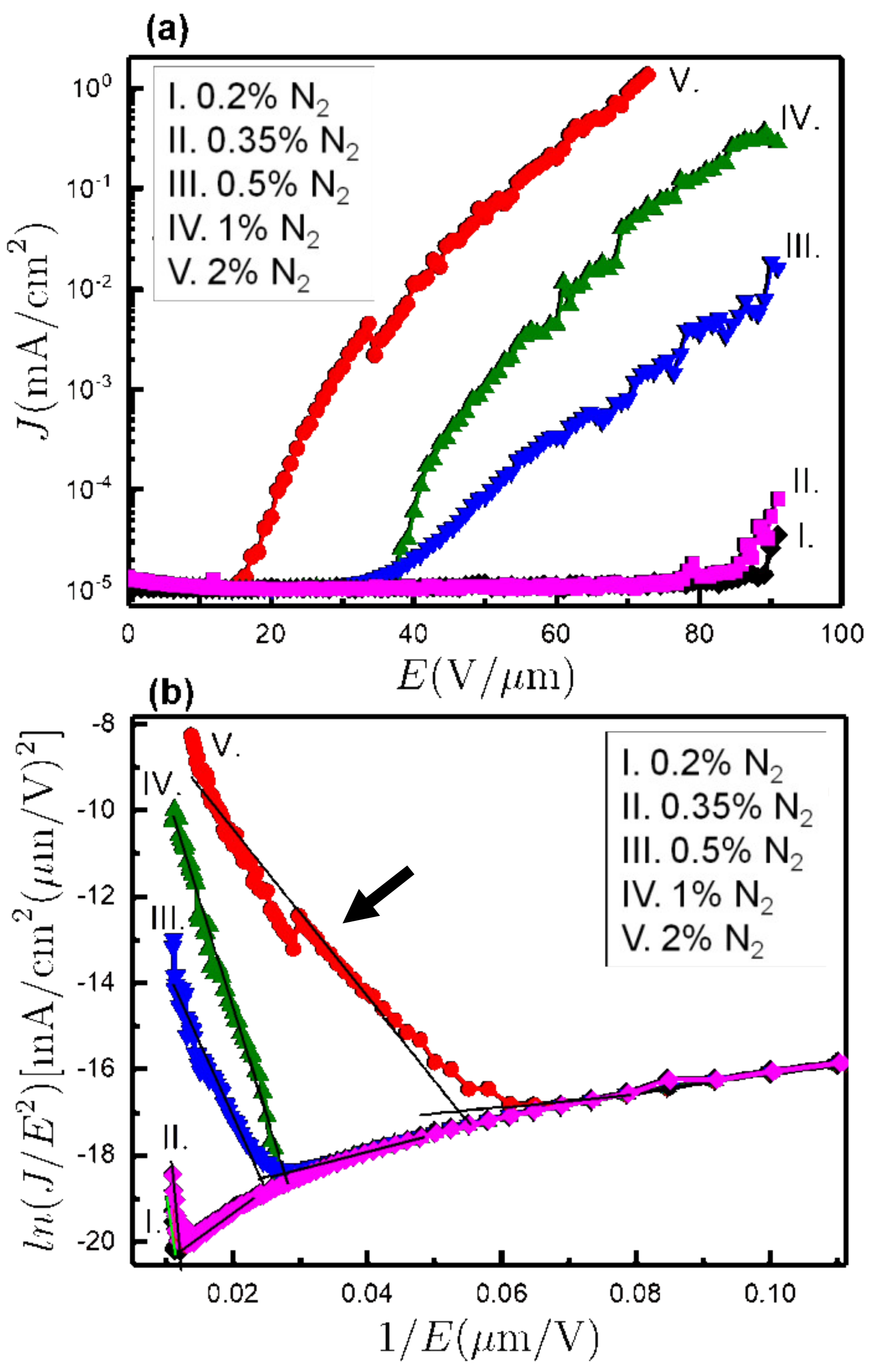
| N2 | E0 (V/µm) | β | J at 53 V/µm |
|---|---|---|---|
| 0.2% | 83.7 | 27 | 1 × 10⁻⁵ (mA/cm2) |
| 0.35% | 88.5 | 12 | 1 × 10⁻⁵ (mA/cm2) |
| 0.5% | 41.0 | 130 | 22 × 10−5 (mA/cm2) |
| 1% | 36.2 | 89 | 26 × 10−4 (mA/cm2) |
| 2% | 18.7 | 230 | 13 × 10−2 (mA/cm2) |
© 2020 by the authors. Licensee MDPI, Basel, Switzerland. This article is an open access article distributed under the terms and conditions of the Creative Commons Attribution (CC BY) license (http://creativecommons.org/licenses/by/4.0/).
Share and Cite
Lloret, F.; Sankaran, K.J.; Millan-Barba, J.; Desta, D.; Rouzbahani, R.; Pobedinskas, P.; Gutierrez, M.; Boyen, H.-G.; Haenen, K. Improved Field Electron Emission Properties of Phosphorus and Nitrogen Co-Doped Nanocrystalline Diamond Films. Nanomaterials 2020, 10, 1024. https://doi.org/10.3390/nano10061024
Lloret F, Sankaran KJ, Millan-Barba J, Desta D, Rouzbahani R, Pobedinskas P, Gutierrez M, Boyen H-G, Haenen K. Improved Field Electron Emission Properties of Phosphorus and Nitrogen Co-Doped Nanocrystalline Diamond Films. Nanomaterials. 2020; 10(6):1024. https://doi.org/10.3390/nano10061024
Chicago/Turabian StyleLloret, Fernando, Kamatchi Jothiramalingam Sankaran, Josué Millan-Barba, Derese Desta, Rozita Rouzbahani, Paulius Pobedinskas, Marina Gutierrez, Hans-Gerd Boyen, and Ken Haenen. 2020. "Improved Field Electron Emission Properties of Phosphorus and Nitrogen Co-Doped Nanocrystalline Diamond Films" Nanomaterials 10, no. 6: 1024. https://doi.org/10.3390/nano10061024
APA StyleLloret, F., Sankaran, K. J., Millan-Barba, J., Desta, D., Rouzbahani, R., Pobedinskas, P., Gutierrez, M., Boyen, H.-G., & Haenen, K. (2020). Improved Field Electron Emission Properties of Phosphorus and Nitrogen Co-Doped Nanocrystalline Diamond Films. Nanomaterials, 10(6), 1024. https://doi.org/10.3390/nano10061024