Communication

Double Metal Oxide Electron Transport Layers for Colloidal Quantum Dot Light-Emitting Diodes

1
Department of Electrical and Computer Engineering, Inter-university Semiconductor Research Center, Seoul National University, Seoul 08826, Korea
2
Department of Electrical Engineering, Pusan National University, Busan 46241, Korea
3
Department of Energy Science, Center for Artificial Atoms, Sungkyunkwan University (SKKU), Suwon, Gyeonggi-do 16419, Korea
4
Department of Electronics Engineering, Sookmyung Women’s University, Seoul 04310, Korea
5
Realistic Media Research Center, Innovative Technology Research Division, Gumi Electronics & Information Technology Research Institute (GERI), Gumi, Gyeonsangbuk-do 39253, Korea
*
Author to whom correspondence should be addressed.
Nanomaterials 2020, 10(4), 726; https://doi.org/10.3390/nano10040726
Submission received: 7 March 2020 / Revised: 7 April 2020 / Accepted: 9 April 2020 / Published: 11 April 2020
(This article belongs to the Section Nanocomposite Materials)

Abstract

:
The performance of colloidal quantum dot light-emitting diodes (QD-LEDs) have been rapidly improved since metal oxide semiconductors were adopted for an electron transport layer (ETL). Among metal oxide semiconductors, zinc oxide (ZnO) has been the most generally employed for the ETL because of its excellent electron transport and injection properties. However, the ZnO ETL often yields charge imbalance in QD-LEDs, which results in undesirable device performance. Here, to address this issue, we introduce double metal oxide ETLs comprising ZnO and tin dioxide (SnO2) bilayer stacks. The employment of SnO2 for the second ETL significantly improves charge balance in the QD-LEDs by preventing spontaneous electron injection from the ZnO ETL and, as a result, we demonstrate 1.6 times higher luminescence efficiency in the QD-LEDs. This result suggests that the proposed double metal oxide ETLs can be a versatile platform for QD-based optoelectronic devices.

Graphical Abstract

1. Introduction

For a few decades, there has been a growing interest in exploiting unique and superior optical properties of colloidal quantum dots (QDs) in various optoelectronic devices [1,2,3,4]. Near-unity photoluminescence quantum yield (PL QY), narrow emission spectral bandwidth with the full width at half maximum around 30 nm, and easily tunable emission wavelength are the attractive features of QDs for display [5,6,7]. Furthermore, low-cost solution processability and flexibility are also appealing properties of QDs to enable next-generation displays. Based on these advantages, the various QDs comprised of II-VI [8,9], III-V [10,11,12], IV [13,14], perovskite [15,16], are actively developing for display application.
The efficiency of QD-based light-emitting diodes (QD-LEDs) has been improved steadily over the past two decades, and one of the most important breakthroughs was made by employing a metal oxide semiconductor in the electron transport layer (ETL). Suitable energy levels and high electron mobility of metal oxide semiconductors led to efficient charge injection and transport, thereby resulting in notable progress in the luminescence efficiency of QD-LEDs [17,18,19,20]. Various types of metal oxide semiconductors have been employed and investigated, and among those metal oxide semiconductors, zinc oxide (ZnO) has been the most widely employed because of their easy processability, excellent electrical properties, and transparency [21,22]. As a result of intensive investigation, the ZnO ETL is now considered as a standard platform for high-performance QD-LEDs, and the state-of-the-art QD-LEDs also employ ZnO-based ETL [10,22].
Although the performance of QD-LEDs has been developed with the ZnO ETL, ZnO has been often indicated as a major cause for undesirable device performance such as the efficiency droop (i.e., a rapid decrease in the efficiency as current density or luminance increase), poor operational stability, and short lifetime. These features are originated from the non-balanced electron and hole densities in the device, which is attributed to excessive electron injection from the ZnO ETL. It is reported that the similar conduction band edge of ZnO to that of QDs often yields spontaneous electron injection, and faster electron mobility of ZnO than hole mobility of typical organic hole-transporting layer (HTL) materials further worsen the charge imbalance [23].
In order to address this issue and improve the charge balance inside the device, various studies have been employed to suppress electron injection from ZnO. One of the most representative approaches is to employ an interlayer between the ZnO ETL and the QD layer [22,24,25,26,27]. Inserting an ultrathin dielectric has been found to be an efficient way to improve the charge balance by reducing the injection rate of electrons and preventing spontaneous injection from ZnO. Diverse organic insulating materials such as poly(methylmethacrylate) (PMMA) [22] and poly(4-vinylpyridine) (PVPy) [24] have been employed and shown their effectiveness. However, employing an insulating interlayer accompanies a careful optimization of the interlayer thickness because the carrier injection through an insulator relies on a direct or Fowler–Nordheim tunneling. Therefore, with the interlayer thicker than the critical thickness, a carrier injection efficiency decreases significantly, resulting in rapid deterioration of device performance.
An alternative approach is to use an n-type organic semiconductor such as poly(9-vinlycarbazole) (PVK) [25], 1,3,5-tris(2-N-phenylbenzimidazolyl)benzene (TPBi) [26], and 4,7-diphenyl-1,10-phenanthroline (Bphen) [27] for the interlayer. In this case, the organic interlayer acts as a second ETL that slows down the injected electrons from ZnO before they reach the QDs. This ‘double ETL’ approach successfully improved the charge balance, but employing organic semiconductors has a drawback in limited processability due to the non-robustness of organic thin films. Therefore, it is necessary to consider other types of materials to construct the double ETL that can efficiently redeem the ZnO-based single ETL while providing unconstrained processability.
In this study, we introduce a double ETL consisting of two types of metal oxide semiconductor to demonstrate the improved performance of QD-LEDs. The double ETL comprises bilayer stacks of ZnO and tin dioxide (SnO2) nanoparticles (NPs), and here, SnO2 NPs are used to supplement the ZnO ETL; the charge imbalance caused by excessive electron injection from ZnO is controlled by the SnO2 second ETL. Employing the material for the second ETL from the library of metal oxide semiconductors has an advantage in processability over organic semiconductors; similar to ZnO NPs, SnO2 NPs produce highly smooth and robust thin films under low temperature. As a result of improved charge balance using the ZnO/SnO2 double ETL, the QD-LED exhibits notable improvement in luminescence efficiency, suggesting that the double metal oxide ETL could be a new platform to achieve high-performance QD-LEDs.

2. Experiments

The SnO2 NPs with a diameter of around 5 nm, dispersed in water, was purchased by MKnano (Missisauga, Canada). The details on the material preparation of ZnO NPs with a diameter of 3−5 nm and CdSe/ZnS QDs with a diameter of 8 nm for red emission are followed by our previous articles [21]. For thermal evaporation, 4,4′,4′′-Tris(carbazol-9-yl)triphenylamine (TCTA) and MoO3, were purchased at Lumtec (New Taipei City, Taiwan) and Al were purchased at iTASCO (Seoul, Republic of Korea). All materials were used as received.
QD-LEDs with the structure of glass/indium tin oxide (ITO)/ETLs (40 nm)/QDs (20 nm)/TCTA (40 nm)/MoO3 (10 nm)/Al (100 nm) were fabricated as following sequence (Figure 1a). The ITO glass substrates were sequentially ultrasonicated with acetone, isopropyl alcohol, and deionized (DI) water and then, dried at 120 °C in an oven for 30 min. For single-layer ETL deposition, 40 nm of ZnO NPs thin films were deposited on the cleaned ITO glass by the spin coating method with 20 mg/mL of ZnO NPs solution dispersed in butanol at 2000 rpm during 60 s. For double-layer ETL deposition, first, 10 mg/mL of ZnO NPs solution dispersed in butanol was spin-coated on the cleaned ITO glass at 2000 rpm during 60 s. The thickness of ZnO NPs for the first ETL was 20 nm. Then, 7.5 mg/mL of SnO2 NPs solution dispersed in DI water was spin-coated on the ZnO NPs film at 2000 rpm during 60 s. The total thickness of the double ETLs was 40 nm. After each spin coating process to deposit ETL, the processed films were dried for 30 min in a 90 °C nitrogen oven. Then, 20 nm thickness of the QD emission layer was deposited on ETLs by spin-coating at 4000 rpm during 30 s, followed by drying in the 70 °C nitrogen oven for 30 min. Then, substrates were moved to the vacuum chamber, and 40 nm thickness of TCTA, 10 nm thickness of MoO3 and 100 nm thickness Al were successively deposited by thermal evaporation method at a pressure below 5 × 10⁻6 Torr. After the deposition, all devices were glass capped with ultraviolet (UV) curing epoxy resin (XNR 5570-B1, Nagase ChemteX Corp., Osaka, Japan) in a nitrogen glove box.
The surface topography and Kelvin probe force microscopy (KPFM) of QDs and NPs were obtained using an atomic force microscope (AFM, XE-100, Park Systems, Suwon, Republic of Korea). The work function of QDs was calculated with calibrating the scanning probe tip with a highly oriented pyrolytic graphite (HOPG). The thickness of thin-film was measured by ellipsometry (MG-1000, Nanoview, Ansan, Republic of Korea). QD-LED performance was characterized by a Keithley 236 source measurement unit and CS-1000A spectroradiometer (Konica-Minolta, Tokyo, Japan).

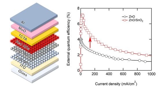
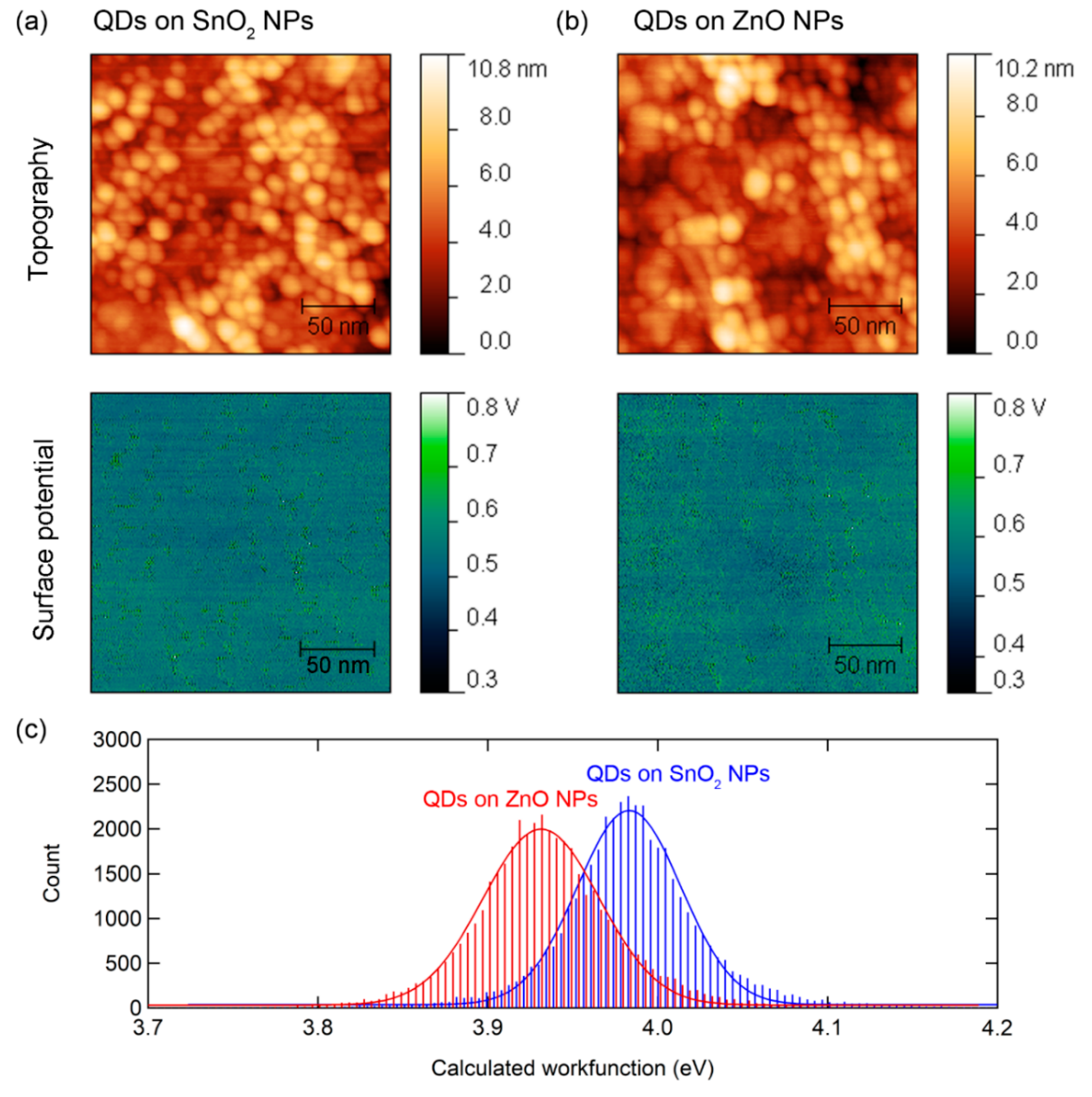
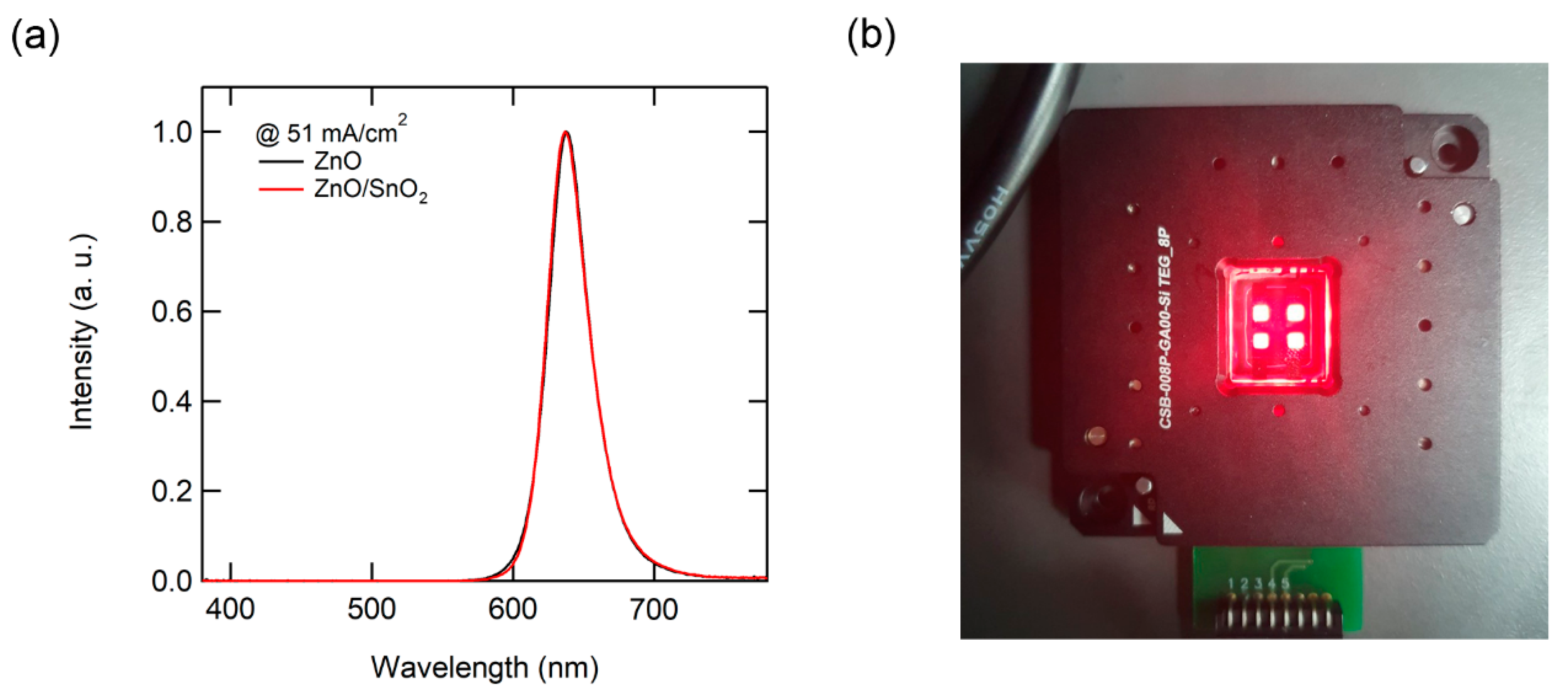
3. Results and Discussion

We chose SnO2 NPs for the second electron injection layer because of their excellent solution processability, high transparency in the visible region (Figure S1), which is similar to ZnO NPs, and decent electron-transport properties as evidenced by the previous employment in perovskite solar cells [28] and organic light-emitting diodes [29]. In addition, in our recent study [20], we have examined the use of SnO2 NPs for the ETL in QD-LEDs, and found out SnO2 NPs have favorable interfacial properties with QDs that do not induce spontaneous electron injection; SnO2 NPs have lower conduction band minimum (CBM) (see Figure 1b) and lower carrier concentration compared to ZnO NPs. In order to take advantage of SnO2 NPs while maintaining an excellent electron transporting ability of the standard ZnO-based ETL, we propose a new ETL platform comprising the stack of ZnO and SnO2 NPs. In this double ETL structure, ZnO NPs are responsible for efficient charge transport, and SnO2 NPs are responsible for balanced electron-hole densities in the QD-LEDs.
Before employing the double metal oxide ETL in the QD-LEDs, we first examined the morphology of the ZnO/SnO2 bilayer stack using atomic force microscope (AFM) measurements and compared them with that of the ZnO film. As shown in Figure S2a,b, the SnO2 coated on the ZnO produce a highly dense thin film with the root-mean-square (RMS) roughness of 6.22 nm which is comparable to the RMS roughness of ZnO film, 4.15 nm. Next, we verified the processability of the ZnO/SnO2 double ETL in terms of robustness and wettability. In the inverted structure, QDs are deposited on the ETL. Thus, it is necessary to have a robust film that is not damaged during QD deposition. Furthermore, having a wettable surface that does not induce dewetting of QD solution is also important to produce smooth thin film. To check these, we deposited QDs on SnO2 film and examined the surface morphology. As a reference sample, we also prepared the QD film coated on ZnO. As shown in Figure S2c,d, as a result of suitable wettability for QD deposition and robustness of SnO2 film, the QDs coated on the SnO2 film form a highly smooth thin film with a low RMS roughness of 2.05 nm, which is similar to the QD film on ZnO (4.33 nm).
To further study the electrical interaction between the metal-oxide and QDs, we measured the KPFM of the QDs on SnO2 and ZnO. KPFM measure the potential offset between a probe tip and a surface by applying alternating current (AC) voltage, which oscillates the AFM probe tip, and variable direct current (DC) voltage to cancel the oscillations, which are equal to the contact potential difference (CPD) between the probe and sample. The potential difference between the probe tip and sample can be expressed in a difference of work function (W) as follows: eVCPD = Wsample − Wtip, where e is the elementary charge. Therefore, we can obtain the work function of samples by calibrating the probe tip with HOPG, which has a work function of 4.475eV as a reference surface [30,31,32]. Figure 2a,b showed the topography and surface potential image of QDs on SnO2 and ZnO. The uniform surface potential images are due to the evenly spread QD films without pinholes. Figure 2c shows the calculated work function of QDs with different metal oxide underlayer. The histogram of work function was fitted with the Gaussian distribution as follows:
f ( x ) = A e x p [ ( x x 0 w i d t h ) 2 ]
As shown in Figure 2c, the QDs on SnO2 had 3.98 eV of center value (x0) and 0.043 eV of width, and the QDs on ZnO had an average of 3.93 eV of x0 and 0.048 eV of width. A work function is the energy of the Fermi level versus the vacuum level; thus, the low work function of QDs on ZnO can be interpreted as the Fermi level rising due to spontaneous electron injection from ZnO to QDs. In this regard, the high work function of QDs on SnO2 is an indication of reduced spontaneous electron injection from the underlying SnO2 layer to QDs. Therefore, it can be expected that the metal oxide ETL will influence on the device performance due to the difference in electrical interaction with QD.
Next, we fabricated QD-LEDs based on the ZnO/SnO2 double ETL. Figure 3a shows the electroluminescence (EL) spectra of QD-LEDs. The EL spectra of QD-LEDs with the ZnO ETL and the ZnO/SnO2 double ETL showed almost identical spectrum shapes, due to the similar optical properties of ZnO and SnO2 (i.e., transparency in the visible range). In addition, both QD-LEDs exhibit pure emission of QDs without any parasitic emission from adjacent SnO2 and TCTA layers. This indicates that electron and hole are injected to QDs without being accumulated at the ETL and HTL interfaces, and the exciton recombination region is well confined in the QD layer. Figure 3b shows uniform emission of 2 × 2 arrays of QD-LEDs over the glass size of 20 × 20 mm2.
Figure 4 and Table 1 compares QD-LED performances with the single ZnO ETL and ZnO/SnO2 double ETLs. Figure 4a shows the current density–luminance–voltage relationship of the QD-LEDs with the ZnO or SnO2/ZnO ETLs. As shown in Figure 4a, the QD-LED with the double ETLs exhibits much better switching behaviors with a lower turn-on voltage and steeper increase in both current density and luminance. The QD-LED with the double ETL also exhibited decreased operating voltage. Note that decrease in operating voltage has never been observed in the previous studies that employed a secondary injection layer to suppress spontaneous electron injection from ZnO [22,24]; Indeed, employing the secondary injection layer often result in an increased operating voltage because of poor electrical properties of the secondary injection layer. This distinguishable result shows the superiority of the proposed ETL platform. All efficiency parameters including external quantum efficiency (EQE, Figure 4b), current efficiency (CE, Figure 4c), and power efficiency (PE, Figure 4d) are greatly improved in the overall current density region with the double ETLs. In particular, the peak EQE of the QD-LEDs was notably increased from 4.11% to 7.16% by using the double ETLs. In the typical CdSe QD-LEDs with an inverted device structure based on the ZnO ETL, charge imbalance is occurred due to the spontaneous electron injection from ZnO, thereby resulting in efficiency deterioration [23]. Therefore, this enhancement in EQE is attributed to the improved electron and hole balance in the QD emission layer by the employment of the SnO2 second ETL. As a result of improved charge balance inside the QD-LEDs, improved current efficiency and power efficiency were also obtained.
In the luminance (L)-voltage (V) characteristic, luminance saturates as the driving voltage increases, which is interpreted as an increase of exciton quenching at a high charge carrier density, resulting in efficiency roll-off. Although the efficiency of QD-LEDs has increased with double ETL, efficiency roll-off still remained. This is caused by the characteristics of thin EMLs, which is comprised of around two monolayers. Further optimization of the EML layer is needed to improve efficiency roll-off, such as increasing the shell thickness of QDs [33] or increasing the thickness of EML through the hybridization of QDs with polymer matrix [34].

4. Conclusions

To summarize, we have introduced double metal oxide ETLs as a new platform to achieve high-performance QD-LEDs. The proposed ETL platform comprises stacks of the primary ZnO ETL and the second ETL comprises SnO2 NPs. The second SnO2 ETL is employed to supplement the standard ZnO ETL in suppressing spontaneous electron injection from ZnO to QDs. With the SnO2 second ETL, charge balance in the QD-LEDs is improved, thereby exhibiting a significant increase in electroluminescence efficiency. The excellent processability and robustness of the proposed double metal oxide ETLs exhibit promising potential as the new platform for QD-based optoelectronic devices.

Supplementary Materials

The following are available online at https://www.mdpi.com/2079-4991/10/4/726/s1: Figure S1: Transmittance spectra of ITO, ZnO NPs and SnO2 NPs.; Figure S2: AFM topology of (a) ZnO NPs, (b) SnO2 NPs on ZnO NPs, (c) QDs on ZnO NPs and (d) QDs on SnO2 NPs.

Author Contributions

Investigating, M.P., J.L. and H.L.; writing—original draft preparation, M.P. and J.R.; writing—review and editing, D.L. All authors have read and agreed to the published version of the manuscript.

Funding

This work was supported by the National Research Foundation of Korea (NRF) grant funded by the Korea government (Ministry of Science and ICT) (NRF-2019R1C1C1005258, NRF-2020R1C1C1013079 and NRF-2019R1C1C1006481).

Conflicts of Interest

The authors declare no conflict of interest.

References

  1. Colvin, V.L.; Schlamp, M.C.; Alivisatos, A.P. Light-emitting diodes made from cadmium selenide nanocrystals and a semiconducting polymer. Nature 1994, 370, 354–357. [Google Scholar] [CrossRef]
  2. Sargent, E.H. Colloidal quantum dot solar cells. Nat. Photonics 2012, 6, 133–135. [Google Scholar] [CrossRef]
  3. Oertel, D.C.; Bawendi, M.G. Photodetectors based on treated CdSe quantum-dot films. Appl. Phys. Lett. 2005, 87, 213505. [Google Scholar] [CrossRef]
  4. Ruan, C.; Zhang, Y.; Lu, M.; Ji, C.; Sun, C.; Chen, X.; Chen, H.; Colvin, V.L.; Yu, W.W. White Light-Emitting Diodes Based on AgInS2/ZnS Quantum Dots with Improved Bandwidth in Visible Light Communication. Nanomaterials 2016, 6, 13. [Google Scholar] [CrossRef] [Green Version]
  5. Yan, C.; Du, X.; Li, J.; Ding, X.; Li, Z.; Tang, Y. Effect of Excitation Wavelength on Optical Performances of Quantum-Dot-Converted Light-Emitting Diode. Nanomaterials 2019, 9, 1100. [Google Scholar] [CrossRef] [Green Version]
  6. Li, J.; Tang, Y.; Li, Z.; Ding, X.; Yu, S.; Yu, B. Improvement in Color-Conversion Efficiency and Stability for Quantum-Dot-Based Light-Emitting Diodes Using a Blue Anti-Transmission Film. Nanomaterials 2018, 8, 508. [Google Scholar] [CrossRef] [Green Version]
  7. Cho, K.-S.; Lee, E.K.; Joo, W.-J.; Jang, E.; Kim, T.-H.; Lee, S.J.; Kim, J.M. High-performance crosslinked colloidal quantum-dot light-emitting diodes. Nat. Photonics 2009, 3, 341–345. [Google Scholar] [CrossRef]
  8. Shirasaki, Y.; Supran, G.J.; Bawendi, M.G.; Bulović, V. Emergence of colloidal quantum-dot light-emitting technologies. Nat. Photonics 2013, 7, 13–23. [Google Scholar] [CrossRef]
  9. Moon, A.; Kim, J. Hybrid Quantum Dot Light-Emitting Diodes for White Emission Using Blue Phosphorescent Organic Molecules and Red Quantum Dots. Micromachines 2019, 10, 609. [Google Scholar] [CrossRef] [Green Version]
  10. Won, Y.-H.; Cho, O.; Kim, T.; Chung, D.-Y.; Kim, T.; Chung, H.; Jang, H.; Lee, J.; Kim, D.; Jang, E. Highly efficient and stable InP/ZnSe/ZnS quantum dot light-emitting diodes. Nature 2019, 575, 634–638. [Google Scholar] [CrossRef]
  11. Lim, J.; Park, M.; Bae, W.K.; Lee, D.; Lee, S.; Lee, C.; Char, K. Highly Efficient Cadmium-Free Quantum Dot Light-Emitting Diodes Enabled by the Direct Formation of Excitons within InP@ZnSeS Quantum Dots. ACS Nano 2013, 7, 9019–9026. [Google Scholar] [CrossRef]
  12. Chen, S.; Tang, M.; Wu, J.; Jiang, Q.; Dorogan, V.; Benamara, M.; Mazur, Y.I.; Salamo, G.J.; Liu, H. Long-Wavelength InAs/GaAs Quantum-Dot Light Emitting Sources Monolithically Grown on Si Substrate. Photonics 2015, 2, 646–658. [Google Scholar] [CrossRef]
  13. Yamada, H.; Shirahata, N. Silicon Quantum Dot Light Emitting Diode at 620 nm. Micromachines 2019, 10, 318. [Google Scholar] [CrossRef] [PubMed] [Green Version]
  14. Ghosh, B.; Shirahata, N. All-Inorganic Red-Light Emitting Diodes Based on Silicon Quantum Dots. Crystals 2019, 9, 385. [Google Scholar] [CrossRef] [Green Version]
  15. Tien, C.-H.; Chen, L.-C.; Lee, K.-Y.; Tseng, Z.-L.; Dong, Y.-S.; Lin, Z.-J. High-Quality All-Inorganic Perovskite CsPbBr3 Quantum Dots Emitter Prepared by a Simple Purified Method and Applications of Light-Emitting Diodes. Energies 2019, 12, 3507. [Google Scholar] [CrossRef] [Green Version]
  16. Lao, X.; Li, X.; Ågren, H.; Chen, G. Highly Controllable Synthesis and DFT Calculations of Double/Triple-Halide CsPbX3 (X = Cl, Br, I) Perovskite Quantum Dots: Application to Light-Emitting Diodes. Nanomaterials 2019, 9, 172. [Google Scholar] [CrossRef] [Green Version]
  17. Caruge, J.M.; Halpert, J.E.; Wood, V.; Bulović, V.; Bawendi, M.G. Colloidal quantum-dot light-emitting diodes with metal-oxide charge transport layers. Nat. Photonics 2008, 2, 247–250. [Google Scholar] [CrossRef]
  18. Lee, C.-Y.; Kuo, Y.P.; Chen, P.-Y.; Lu, H.H.; Lin, M.Y. Influence of Annealing Temperature on Weak-Cavity Top-Emission Red Quantum Dot Light Emitting Diode. Nanomaterials 2019, 9, 1639. [Google Scholar] [CrossRef] [Green Version]
  19. Oh, S.; Kim, J. Correlation between the Morphology of ZnO Layers and the Electroluminescence of Quantum Dot Light-Emitting Diodes. App. Sci. 2019, 9, 4539. [Google Scholar] [CrossRef] [Green Version]
  20. Park, M.; Song, J.; An, M.; Lim, J.; Lee, C.; Roh, J.; Lee, D. Colloidal quantum dot light-emitting diodes employing solution-processable tin dioxide nanoparticles in an electron transport layer. RSC Adv. 2020, 10, 8261–8265. [Google Scholar] [CrossRef]
  21. Kwak, J.; Bae, W.K.; Lee, D.; Park, I.; Lim, J.; Park, M.; Cho, H.; Woo, H.; Yoon, D.Y.; Char, K.; et al. Bright and Efficient Full-Color Colloidal Quantum Dot Light-Emitting Diodes Using an Inverted Device Structure. Nano Lett. 2012, 12, 2362–2366. [Google Scholar] [CrossRef] [PubMed]
  22. Dai, X.; Zhang, Z.; Jin, Y.; Niu, Y.; Cao, H.; Liang, X.; Chen, L.; Wang, J.; Peng, X. Solution-processed, high-performance light-emitting diodes based on quantum dots. Nature 2014, 515, 96–99. [Google Scholar] [CrossRef]
  23. Bae, W.K.; Park, Y.-S.; Lim, J.; Lee, D.; Padilha, L.A.; McDaniel, H.; Robel, I.; Lee, C.; Pietryga, J.M.; Klimov, V.I. Controlling the influence of Auger recombination on the performance of quantum-dot light-emitting diodes. Nat. Commun. 2013, 4, 2661. [Google Scholar] [CrossRef] [PubMed] [Green Version]
  24. Yun, J.; Kim, J.; Jang, H.-K.; Lee, K.J.; Seo, J.H.; Jung, B.J.; Kim, G.; Kwak, J. Controlling charge balance using non-conjugated polymer interlayer in quantum dot light-emitting diodes. Org. Electron. 2017, 50, 82–86. [Google Scholar] [CrossRef]
  25. Fu, Y.; Jiang, W.; Kim, D.; Lee, W.; Chae, H. Highly Efficient and Fully Solution-Processed Inverted Light-Emitting Diodes with Charge Control Interlayers. ACS Appl. Mater. Interfaces 2018, 10, 17295–17300. [Google Scholar] [CrossRef]
  26. Park, M.; Song, J.; Jung, H.; An, M.; Lim, J.; Lee, C.; Roh, J.; Lee, D. Improving Performance of Inverted Blue QD-LEDs by Adopting Organic/Inorganic Double Electron Transport Layer. Phys. Status Solidi RRL 2020, 1900737. [Google Scholar] [CrossRef]
  27. Park, M.; Lim, J.; Kwon, Y.; Jung, H.; Kwak, J.; Char, K.; Lee, S.; Lee, C. Improved Performance of Quantum Dot Light Emitting Diodes by Using Charge Blocking Layer. SID Symp. Dig. Tech. Papers 2014, 45, 1309–1311. [Google Scholar] [CrossRef]
  28. Jiang, Q.; Zhang, X.; You, J. SnO2: A Wonderful Electron Transport Layer for Perovskite Solar Cells. Small 2018, 14, 1801154. [Google Scholar] [CrossRef]
  29. Lee, H.; Kang, C.-M.; Park, M.; Kwak, J.; Lee, C. Improved Efficiency of Inverted Organic Light-Emitting Diodes Using Tin Dioxide Nanoparticles as an Electron Injection Layer. ACS Appl. Mater. Interfaces 2013, 5, 1977–1981. [Google Scholar] [CrossRef] [PubMed]
  30. Vasić, B.; Aškrabić, S.; Jakovljević, M.M.; Artemyev, M. Local electrical properties and charging/discharging of CdSe/CdS core-shell nanoplatelets. Appl. Surf. Sci. 2020, 513, 145822. [Google Scholar] [CrossRef]
  31. Benetti, D.; Cui, D.; Zhao, H.; Rosei, F.; Vomiero, A. Direct Measurement of Electronic Band Structure in Single Quantum Dots of Metal Chalcogenide Composites. Small 2018, 14, 1801668. [Google Scholar] [CrossRef]
  32. Hansen, W.N.; Hansen, G.J. Standard reference surfaces for work function measurements in air. Surf. Sci. 2001, 481, 172–184. [Google Scholar] [CrossRef]
  33. Lim, J.; Park, Y.-S.; Wu, K.; Yun, H.J.; Klimov, V.I. Droop-Free Colloidal Quantum Dot Light-Emitting Diodes. Nano Lett. 2018, 18, 6645–6653. [Google Scholar] [CrossRef] [PubMed]
  34. Bae, W.K.; Lim, J.; Zorn, M.; Kwak, J.; Pakr, Y.-S.; Lee, D.; Lee, S.; Char, K.; Zentel, R.; Lee, C. Reduced efficiency roll-off in light-emitting diodes enabled by quantum dot–conducting polymer nanohybrids. J. Mater. Chem. C 2014, 2, 4974–4979. [Google Scholar] [CrossRef]
Figure 1. (a) Device structure and (b) energy band diagram of quantum dot light-emitting diodes (QD-LEDs).
Nanomaterials 10 00726 g001
Figure 2. Atomic force microscopy (AFM) topology and surface potential of red QDs on (a) SnO2 nanoparticles (NPs) and (b) ZnO NPs. (c) Calculated histogram of the work function of QDs from the surface potential signal with various metal-oxide underlayer. Solid lines denote fitting results with Gaussian distribution.
Nanomaterials 10 00726 g002
Figure 3. (a) Electroluminescence (EL) spectra of QD-LEDs with ZnO and SnO2/ZnO double electron transport layer (ETL), and (b) operating device image of QD-LEDs with SnO2/ZnO double ETL.
Nanomaterials 10 00726 g003
Figure 4. (a) Current density (J)-voltage (V)-luminance (L), (b) external quantum efficiency (EQE)-J (c) current efficiency (CE)-J and (d) power efficiency (PE)-J curves of QD-LEDs with ZnO and SnO2/ZnO double ETL.
Nanomaterials 10 00726 g004
Table 1. QD-LED performances with with ZnO and SnO2/ZnO double ETL.
ParameterZnO NPs (40 nm)SnO2 NPs/ZnO NPs (20 nm)/(20 nm)
J (mA/cm2) @ 5 V33.780.44
L (cd/m2) @ 5 V8483061
CEmax (cd/A)3.25.31
EQEmax (%)4.117.16
PEmax (lm/W)3.864.32

