Formation of Size and Density Controlled Nanostructures by Galvanic Displacement

 ,
,  , and
, and
Abstract

1. Introduction
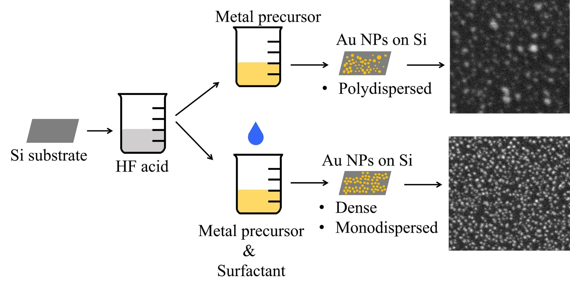
2. Materials and Methods
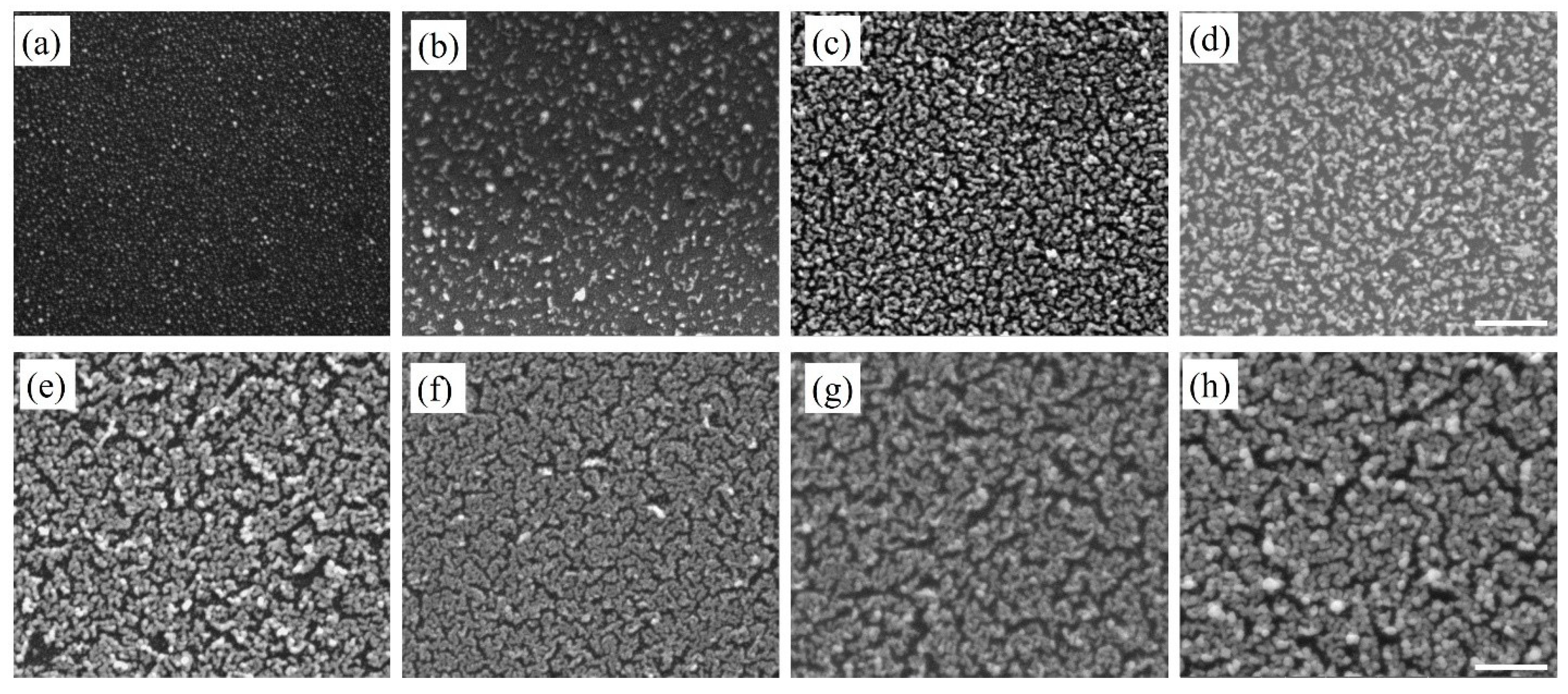
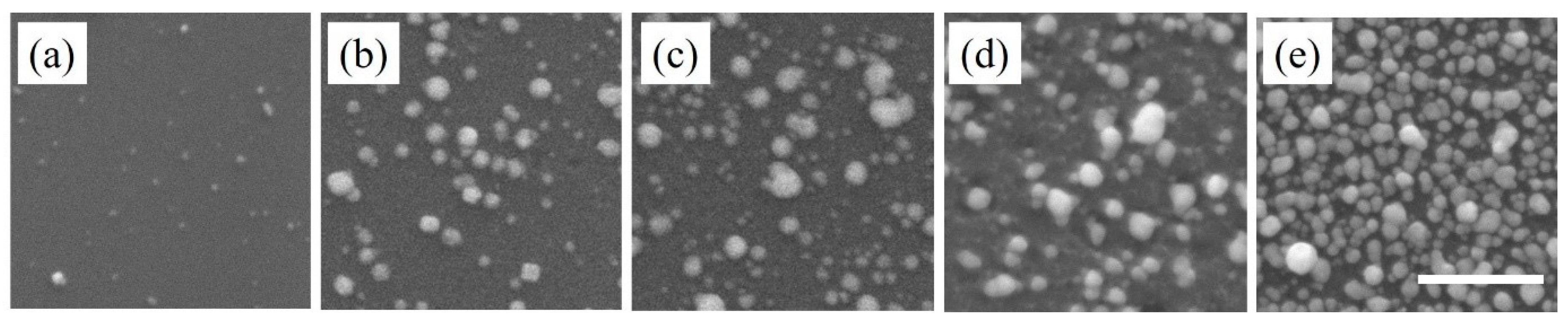
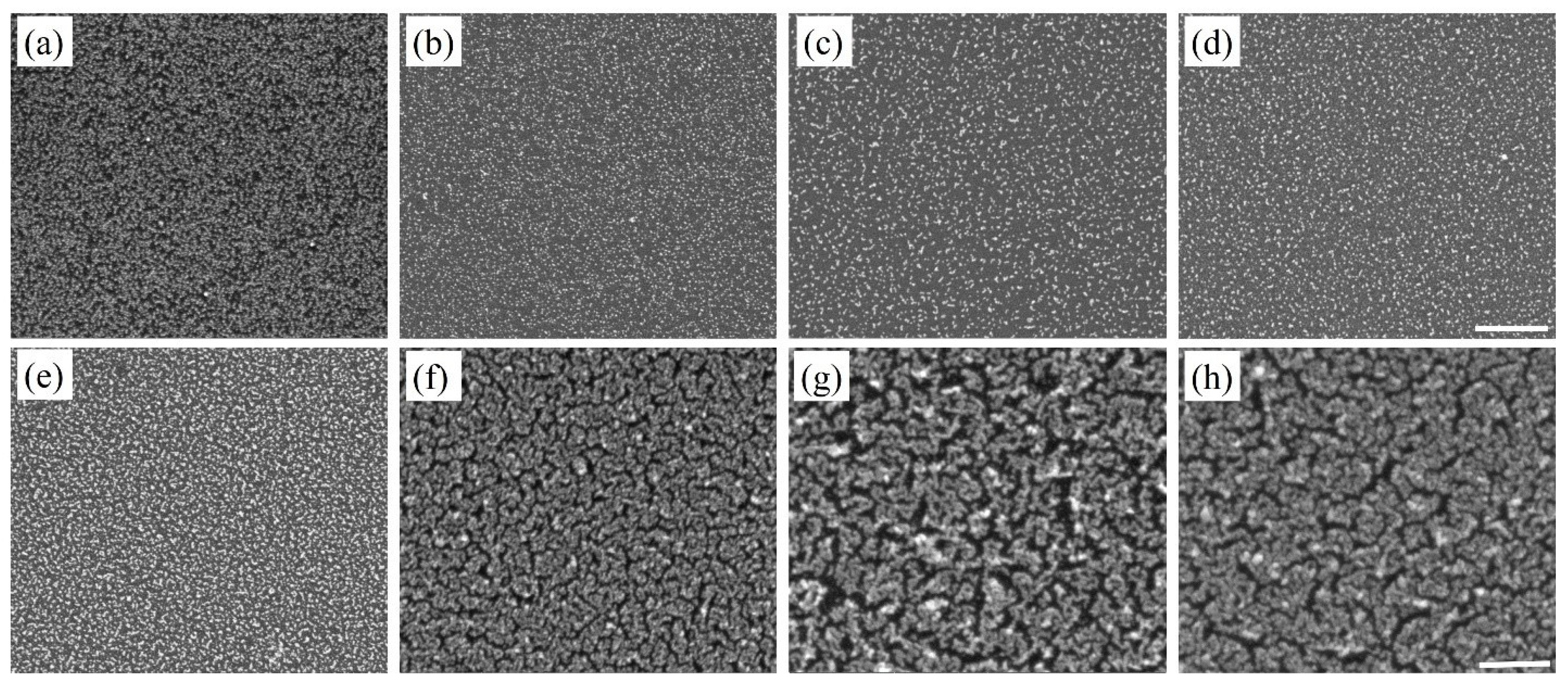
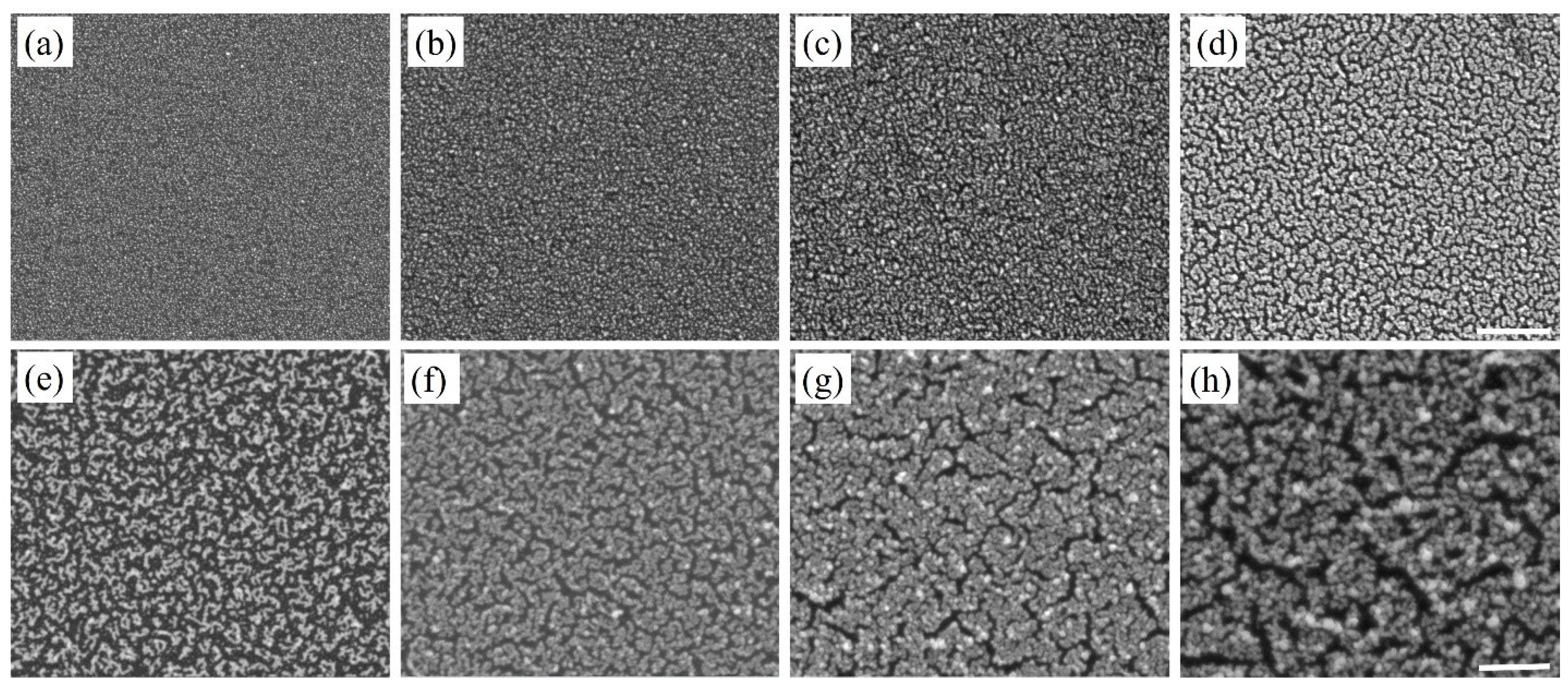
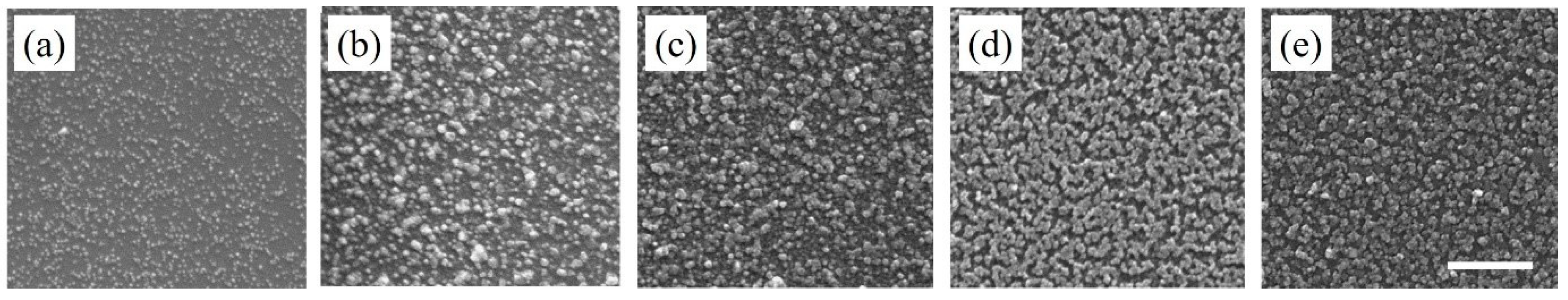
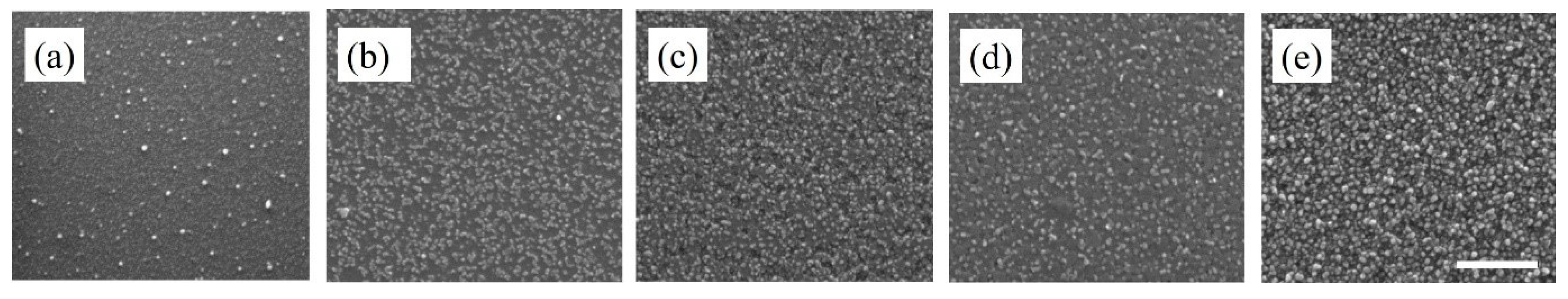
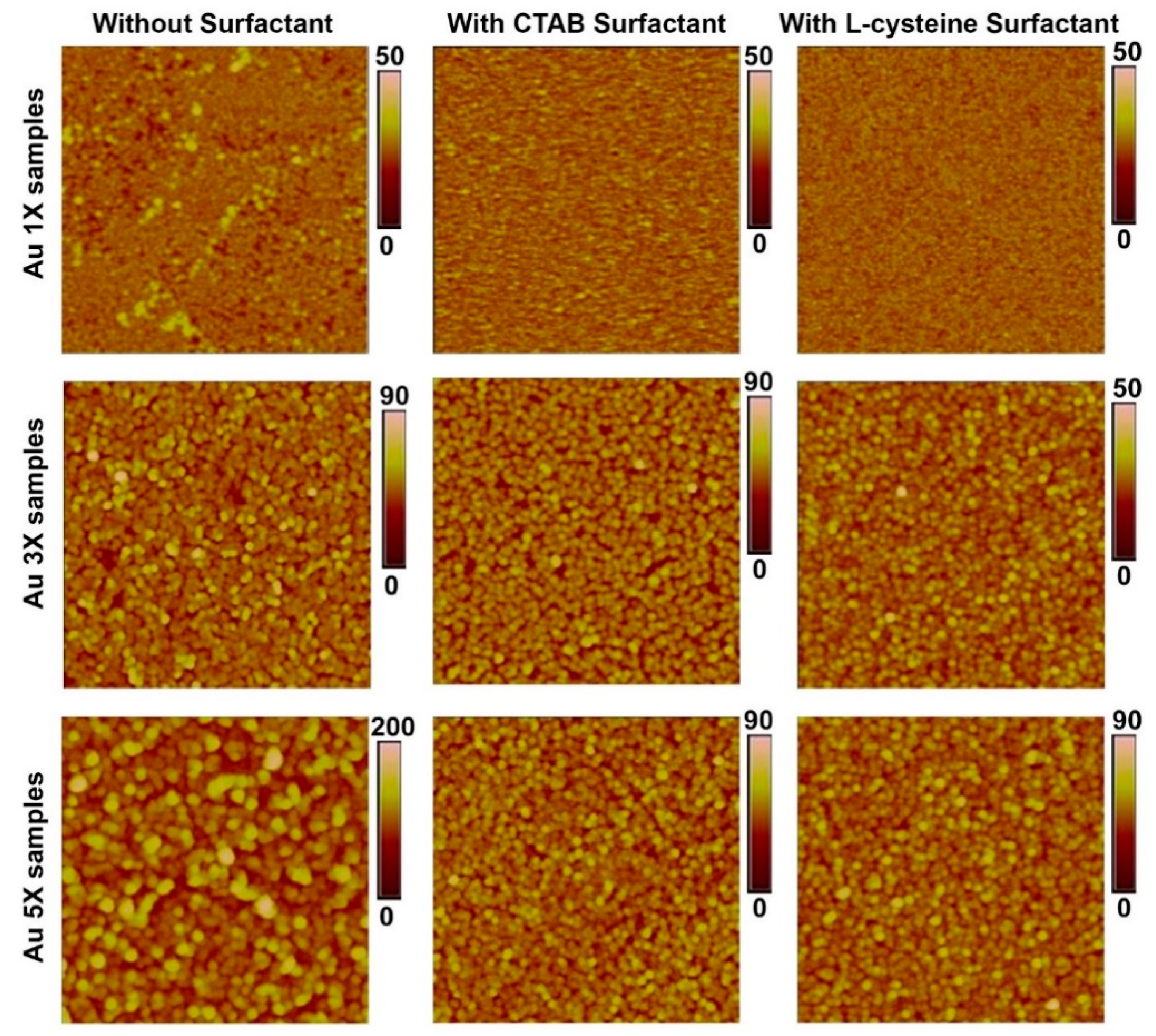
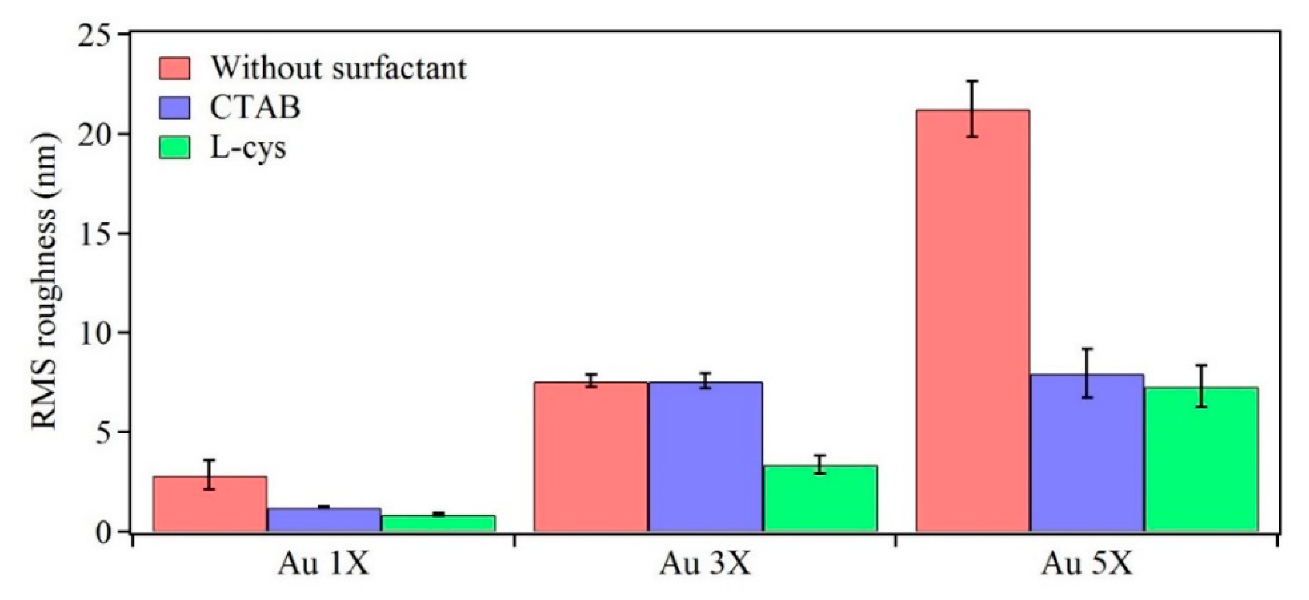
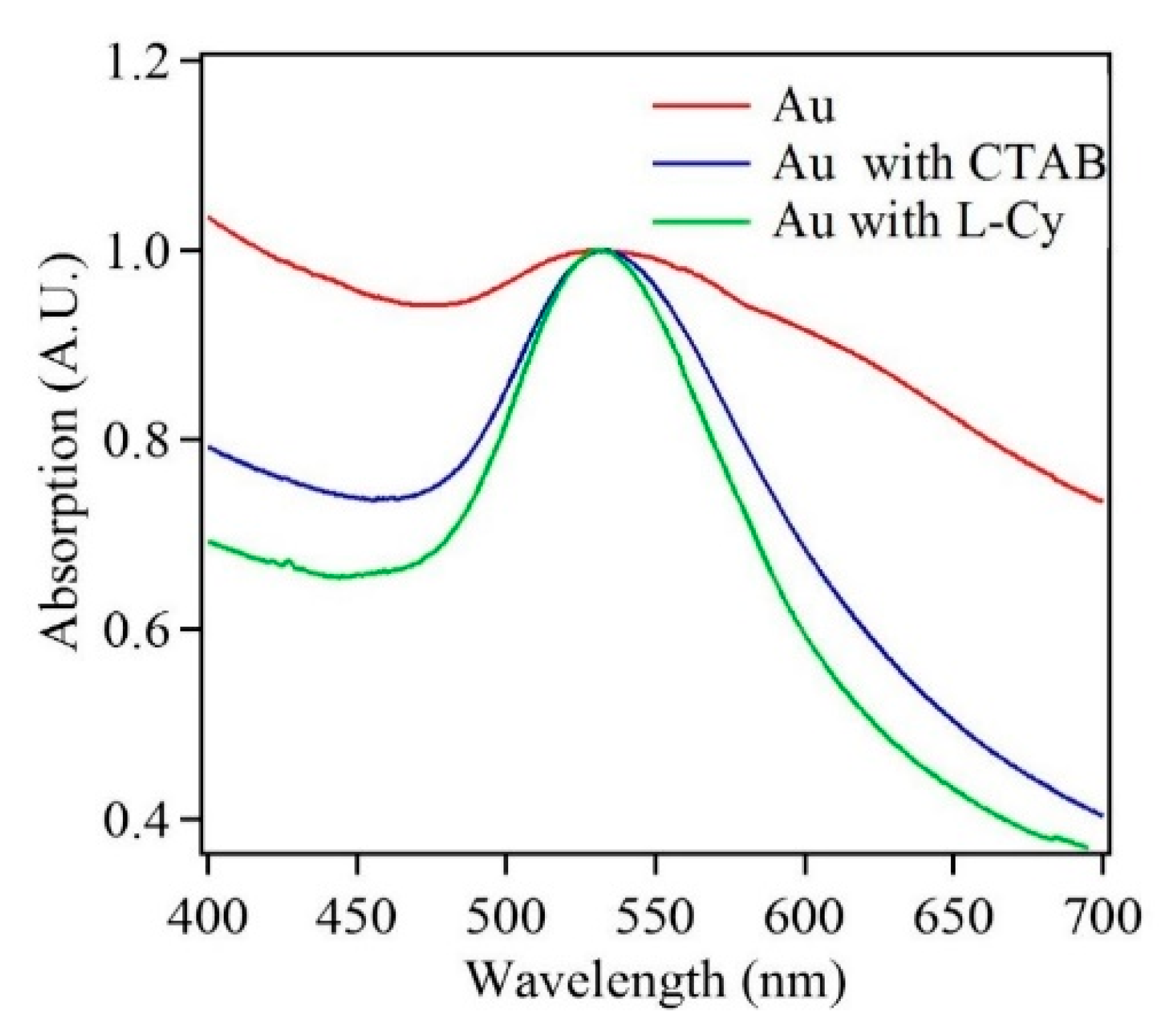
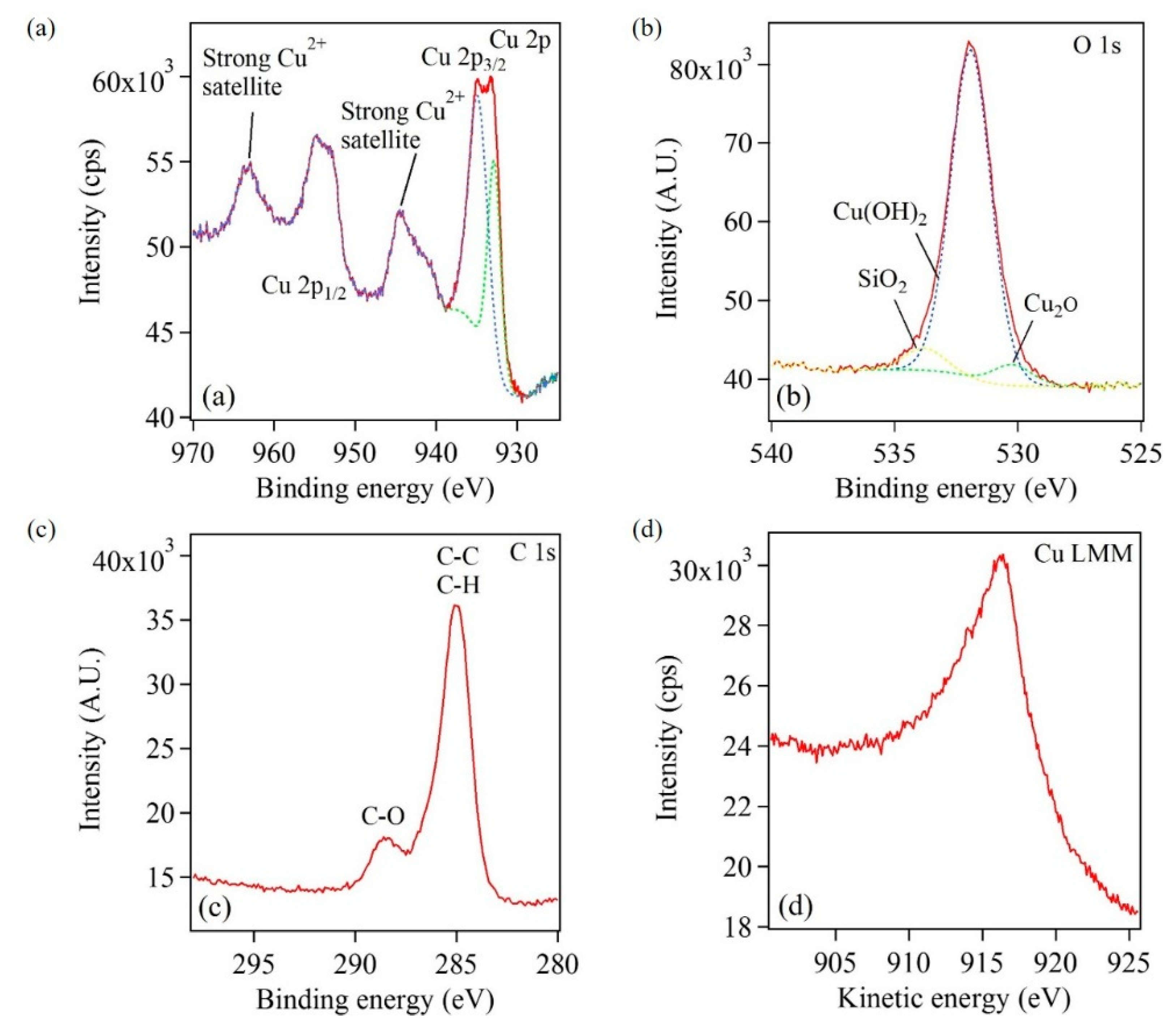
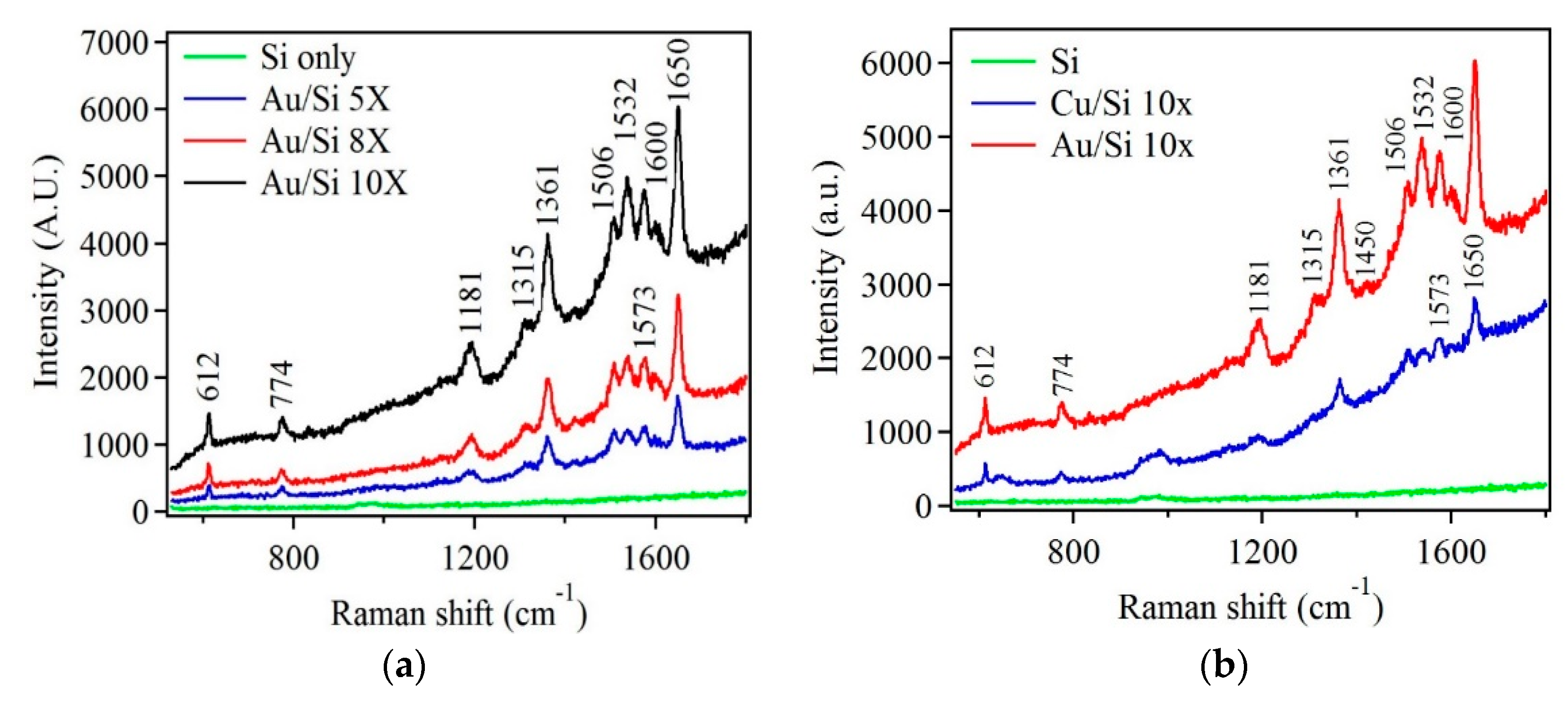
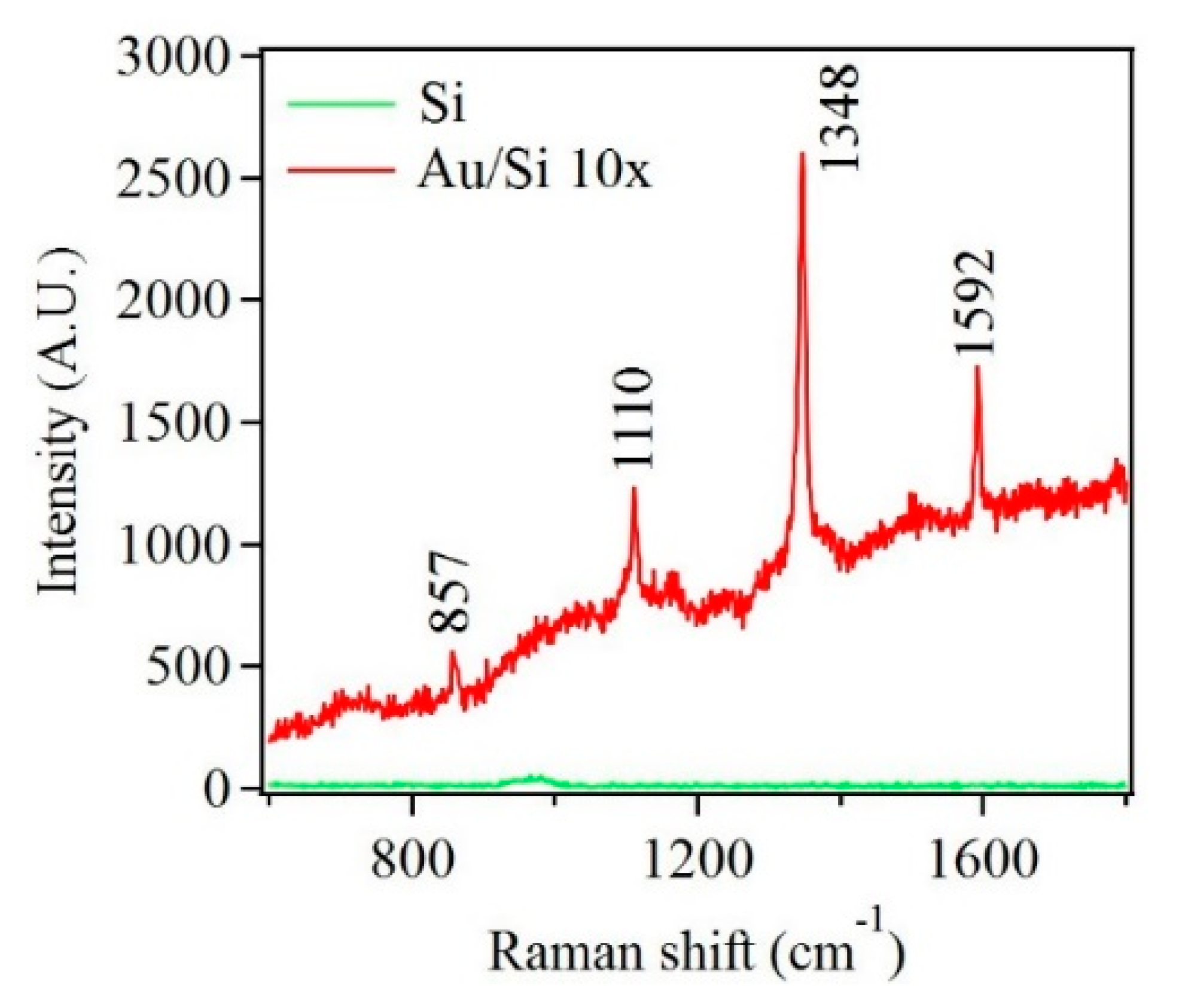
3. Results and Discussion
4. Conclusions
Supplementary Materials
Author Contributions
Funding
Acknowledgments
Conflicts of Interest
References
- Carraro, C.; Maboudian, R.; Magagnin, L. Metallization and nanostructuring of semiconductor surfaces by galvanic displacement processes. Surf. Sci. Rep. 2007, 62, 499–525. [Google Scholar] [CrossRef]
- Ali, H.O.; Christie, I.R.A. A review of electroless gold deposition processes. Gold Bull. 1984, 17, 118–127. [Google Scholar] [CrossRef]
- Gutes, A.; Carraro, C.; Maboudian, R. Ultrasmooth Gold Thin Films by Self-Limiting Galvanic Displacement on Silicon. ACS Appl. Mater. Interfaces 2011, 3, 1581–1584. [Google Scholar] [CrossRef] [PubMed]
- Sayed, S.Y.; Buriak, J.M. Epitaxial Growth of Nanostructured Gold Films on Germanium via Galvanic Displacement. ACS Appl. Mater. Interfaces 2010, 2, 3515–3524. [Google Scholar] [CrossRef] [PubMed]
- Darosa, C.I.; Iglesia, E.; Maboudian, R. Dynamics of Copper Deposition onto Silicon by Galvanic Displacement. J. Electrochem. Soc. 2008, 155, 6. [Google Scholar] [CrossRef]
- Yae, S.; Nasu, N.; Matsumoto, K.; Hagihara, T.; Fukumuro, N.; Matsuda, H. Nucleation behavior in electroless displacement deposition of metals on silicon from hydrofluoric acid solutions. Electrochim. Acta 2007, 53, 35–41. [Google Scholar] [CrossRef]
- Warren, S.; Reitzle, A.; Kazimirov, A.; Ziegler, J.C.; Bunk, O.; Cao, L.X.; Renner, F.U.; Kolb, D.M.; Bedzyk, M.J.; Zegenhagen, J. A structure study of the electroless deposition of Au on Si(1 1 1):H. Surf. Sci. 2002, 496, 287–298. [Google Scholar] [CrossRef]
- Peng, K.; Zhu, J. Morphological selection of electroless metal deposits on silicon in aqueous fluoride solution. Electrochim. Acta 2004, 49, 2563–2568. [Google Scholar] [CrossRef]
- Magagnin, L.; Maboudian, R.; Carraro, C. Gold Deposition by Galvanic Displacement on Semiconductor Surfaces: Effect of Substrate on Adhesion. J. Phys. Chem. B 2002, 106, 401–407. [Google Scholar] [CrossRef]
- Zhang, X.; Qiao, Y.; Xu, L.; Buriak, L. Constructing Metal-Based Structures on Nanopatterned Etched Silicon. ACS Nano 2011, 5, 5015–5024. [Google Scholar] [CrossRef]
- Aizawa, M.; Buriak, J. Nanoscale Patterning of Two Metals on Silicon Surfaces Using an ABC Triblock Copolymer Template. J. Am. Chem. Soc. 2006, 128, 5877–5886. [Google Scholar] [CrossRef] [PubMed]
- Fabre, B.; Hennous, L.; Ababou-Girard, S.; Meriadec, C. Electroless Patterned Assembly of Metal Nanoparticles on Hydrogen-Terminated Silicon Surfaces for Applications in Photoelectrocatalysis. ACS Appl. Mater. Interfaces 2013, 5, 338–343. [Google Scholar] [CrossRef] [PubMed]
- Gorostiza, P.; Allongue, P.; Diaz, R.; Morante, J.; Sanz, F. Electrochemical Characterization of the Open-Circuit Deposition of Platinum on Silicon from Fluoride Solutions. J. Phys. Chem. B 2003, 107, 6454–6461. [Google Scholar] [CrossRef]
- Zhang, Y.; Ang, S.S.; Tay, A.A.O.; Xu, D.; Kang, E.T.; Neoh, K.G.; Chong, L.P.; Huan, A.C.H. Characterization of Electrolessly Deposited Copper and Nickel Nanofilms on Modified Si(100) Surface. Langmuir 2003, 19, 6802–6806. [Google Scholar] [CrossRef]
- Cho, J.S.H.; Kang, H.-K.; Wong, S.S.; Shacham-Diamand, Y. Electroless Cu for VLSI. MRS Bull. 1993, 18, 31–38. [Google Scholar] [CrossRef]
- Scheck, C.; Liu, Y.; Evans, P.; Schad, R.; Bowers, A.; Zangari, G.; Williams, J.; Issacs-Smith, T. Photoexcited electrodeposition of Cu structures on p-Si(001). J. Vac. Sci. Technol. A 2004, 22, 1842–1846. [Google Scholar] [CrossRef]
- Lim, S.; Mo, R.; Pianetta, P.; Chidsey, C. Effect of Silicon Surface Termination on Copper Deposition in Deionized Water. J. Electrochem. Soc. 2001, 148, C16–C20. [Google Scholar] [CrossRef]
- Porter, L.; Choi, H.; Schmeltzer, J.; Ribbe, A.; Elliott, L.; Buriak, J. Electroless Nanoparticle Film Deposition Compatible with Photolithography, Microcontact Printing, and Dip-Pen Nanolithography Patterning Technologies. Nano Lett. 2002, 2, 1369–1372. [Google Scholar] [CrossRef]
- Yang, X.; Zhong, H.; Zhu, Y.; Shen, J.; Li, C. Ultrasensitive and recyclable SERS substrate based on Au-decorated Si nanowire arrays. Dalton Trans. 2013, 42, 14324–14330. [Google Scholar] [CrossRef]
- Lahiri, A.; Wen, R.; Kuimalee, S.; Kobayashi, S.; Park, H. One-step growth of needle and dendritic gold nanostructures on silicon for surface enhanced Raman scattering. Crystengcomm 2012, 14, 1241–1246. [Google Scholar] [CrossRef]
- Blackwood, D.; Khoo, S. Electroless plating of noble metal nanoparticles for improved performance of silicon photodiodes via surface plasmon resonance. Sol. Energy Mater. Sol. Cells 2010, 94, 1201–1206. [Google Scholar] [CrossRef]
- Yu, P.; Chiu, C.; Wu, Y.; Yen, H.; Chen, J.; Kao, C.; Yang, H.; Kuo, H.; Lu, T.; Yeh, W.; et al. Strain relaxation induced microphotoluminescence characteristics of a single InGaN-based nanopillar fabricated by focused ion beam milling. Appl. Phys. Lett. 2008, 93, 081110. [Google Scholar] [CrossRef]
- Kye, J.; Shin, M.; Lim, B.; Jang, J.; Oh, I.; Hwang, S. Platinum Monolayer Electrocatalyst on Gold Nanostructures on Silicon for Photoelectrochemical Hydrogen Evolution. ACS Nano 2013, 7, 6017–6023. [Google Scholar] [CrossRef] [PubMed]
- Rosenberg, R.; Edelstein, D.; Hu, C.; Rodbell, K. Copper Metallization for High Performance Silicon Technology. Annu. Rev. Mater. Sci. 2000, 30, 229–262. [Google Scholar] [CrossRef]
- Pai, P.L.; Ting, C.H. Selective electroless copper for VLSI interconnection. IEEE Electron Device Lett. 1989, 10, 423–425. [Google Scholar] [CrossRef]
- Peng, Z.; Hu, H.; Utama, M.; Wong, L.; Ghosh, K.; Chen, R.; Wang, S.; Shen, Z.; Xiong, Q. Heteroepitaxial Decoration of Ag Nanoparticles on Si Nanowires: A Case Study on Raman Scattering and Mapping. Nano Lett. 2010, 10, 3940–3947. [Google Scholar] [CrossRef] [PubMed]
- Chen, R.; Li, D.; Hu, H.; Zhao, Y.; Wang, Y.; Wong, N.; Wang, S.; Zhang, Y.; Hu, J.; Shen, Z.; et al. Tailoring Optical Properties of Silicon Nanowires by Au Nanostructure Decorations: Enhanced Raman Scattering and Photodetection. J. Phys. Chem. C 2012, 116, 4416–4422. [Google Scholar] [CrossRef]
- Li, M.; Sui, M.; Pandey, P.; Zhang, Q.; Kim, E.; Lee, J. Systematic Control of Self-Assembled Au Nanoparticles and Nanostructures Through the Variation of Deposition Amount, Annealing Duration, and Temperature on Si (111). Nanoscale Res. Lett. 2015, 10, 1–14. [Google Scholar] [CrossRef]
- Vitos, L.; Ruban, A.; Skriver, H.; Kollar, J. The surface energy of metals. Surf. Sci. 1998, 411, 186–202. [Google Scholar] [CrossRef]
- Grzelczak, M.; Perez-Juste, J.; Mulvaney, P.; Liz-Marzan, L. Shape control in gold nanoparticle synthesis. Chem. Soc. Rev. 2008, 37, 1783–1791. [Google Scholar] [CrossRef]
- Love, J.C.; Estroff, L.A.; Kriebel, J.K.; Nuzzo, R.G.; Whitesides, G.M. Self-Assembled Monolayers of Thiolates on Metals as a Form of Nanotechnology. Chem. Rev. 2005, 105, 1103–1170. [Google Scholar] [CrossRef] [PubMed]
- Padalkar, S.; Capadona, J.; Rowan, S.; Weder, C.; Won, Y.; Stanciu, L.; Moon, R. Natural Biopolymers: Novel Templates for the Synthesis of Nanostructures. Langmuir 2010, 26, 8497–8502. [Google Scholar] [CrossRef] [PubMed]
- Padalkar, S.; Capadona, J.; Rowan, S.; Weder, C.; Moon, R.; Stanciu, L. Self-assembly and alignment of semiconductor nanoparticles on cellulose nanocrystals. J. Mater. Sci. 2011, 46, 5672–5679. [Google Scholar] [CrossRef]
- Zhang, W.-W.; Lu, C.-S.; Zou, Y.; Xie, J.-L.; Ren, X.-M.; Zhu, H.-Z.; Meng, Q.-J. Self-Assembly of L-Cysteine-Copper(II)/Copper(I) Multilayer Thin Films on Gold. J. Colloid Interface Sci. 2002, 249, 301–306. [Google Scholar] [CrossRef]
- Sakai, N.; Fujiwara, Y.; Arai, M.; Yu, K.; Tatsuma, T. Electrodeposition of gold nanoparticles on ITO: Control of morphology and plasmon resonance-based absorption and scattering. J. Electroanal. Chem. 2009, 628, 7–15. [Google Scholar] [CrossRef]
- Bhanushali, S.; Ghosh, P.; Ganesh, A.; Cheng, W. 1D Copper Nanostructures: Progress, Challenges and Opportunities. Small 2015, 11, 1232–1252. [Google Scholar] [CrossRef]
- Nikoobakht, B.; El-Sayed, M. Preparation and Growth Mechanism of Gold Nanorods (NRs) Using Seed-Mediated Growth Method. Chem. Mater. 2003, 15, 1957–1962. [Google Scholar] [CrossRef]
- Brust, M.; Blass, P.; Bard, A. Self-Assembly of Photoluminescent Copper(I)−Dithiol Multilayer Thin Films and Bulk Materials. Langmuir 1997, 13, 5602–5607. [Google Scholar] [CrossRef]
- Li, B.; Xie, Y.; Xue, Y. Controllable Synthesis of CuS Nanostructures from Self-Assembled Precursors with Biomolecule Assistance. J. Phys. Chem. C 2007, 111, 12181–12187. [Google Scholar] [CrossRef]
- Brinas, R.; Hu, M.; Qian, L.; Lymar, E.; Hainfeld, J. Gold Nanoparticle Size Controlled by Polymeric Au(I) Thiolate Precursor Size. J. Am. Chem. Soc. 2008, 130, 975–982. [Google Scholar] [CrossRef]
- Bunton, C.A.; Nome, F.; Quina, F.H.; Romsted, L.S. Ion binding and reactivity at charged aqueous interfaces. Acc. Chem. Res. 1991, 24, 357–364. [Google Scholar] [CrossRef]
- Tang, J.; Huang, J.; Man, S. Preparation of gold nanoparticles by surfactant-promoted reductive reaction without extra reducing agent. Spectrochim. Acta A 2013, 103, 349–355. [Google Scholar] [CrossRef] [PubMed]
- Zhou, M.; Wang, B.; Rozynek, Z.; Xie, Z.; Fossum, J.; Yu, X.; Raaen, S. Minute synthesis of extremely stable gold nanoparticles. Nanotechnology 2009, 20, 505606. [Google Scholar] [CrossRef] [PubMed]
- Link, S.; El-Sayed, M. Spectral Properties and Relaxation Dynamics of Surface Plasmon Electronic Oscillations in Gold and Silver Nanodots and Nanorods. J. Phys. Chem. B 1999, 103, 8410–8426. [Google Scholar] [CrossRef]
- Biesinger, M.; Lau, L.; Gerson, A.; Smart, R. Resolving surface chemical states in XPS analysis of first row transition metals, oxides and hydroxides: Sc, Ti, V., Cu and Zn. Appl. Surf. Sci. 2010, 257, 887–898. [Google Scholar] [CrossRef]
- Mcintyre, N.S.; Cook, M.G. X-ray photoelectron studies on some oxides and hydroxides of cobalt, nickel, and copper. Anal. Chem. 1975, 47, 2208–2213. [Google Scholar] [CrossRef]
- Mcintyre, N.S.; Sunder, S.; Shoesmith, D.W.; Stanchell, F.W. Chemical information from XPS—Applications to the analysis of electrode surfaces. J. Vac. Sci. Technol. 1981, 18, 714–721. [Google Scholar] [CrossRef]
- Ma, Q.; Hofmann, J.; Litke, A.; Hensen, E. Cu2O photoelectrodes for solar water splitting: Tuning photoelectrochemical performance by controlled faceting. Sol. Energy Mater. Sol. Cells 2015, 141, 178–186. [Google Scholar] [CrossRef]
- Chavez, K.; Hess, D. A novel method of etching copper oxide using acetic acid. J. Electrochem. Soc. 2001, 148, G640–G643. [Google Scholar] [CrossRef]
- Baklanov, M.; Shamiryan, D.; Tokei, Z.; Beyer, G.; Conard, T.; Vanhaelemeersch, S.; Maex, K. Characterization of Cu surface cleaning by hydrogen plasma. J. Vac. Sci. Technol. B 2001, 19, 1201–1211. [Google Scholar] [CrossRef]
- Panigrahi, S.; Kundu, S.; Basu, S.; Praharaj, S.; Jana, S.; Pande, S.; Ghosh, S.; Pal, A.; Pal, T. Cysteine functionalized copper organosol: Synthesis, characterization and catalytic application. Nanotechnology 2006, 17, 5461–5468. [Google Scholar] [CrossRef]
- Bicer, M.; Sisman, I. Controlled synthesis of copper nano/microstructures using ascorbic acid in aqueous CTAB solution. Powder Technol. 2010, 198, 279–284. [Google Scholar] [CrossRef]
- Israelsen, N.D.; Hanson, C.; Vargis, E. Nanoparticle properties and synthesis effects on surface-enhanced Raman scattering enhancement factor: An introduction. Sci. World J. 2015, 2015, 1–12. [Google Scholar] [CrossRef] [PubMed]
- Sharma, B.; Frontiera, R.; Henry, A.; Ringe, E.; Van Duyne, R. SERS: Materials, applications, and the future. Mater. Today 2012, 15, 16–25. [Google Scholar] [CrossRef]
- Yamamoto, Y.; Hasegawa, K.; Hasegawa, Y.; Takahashi, N.; Kitahama, Y.; Fukuoka, S.; Murase, N.; Baba, Y.; Ozaki, Y.; Itoh, T. Direct conversion of silver complexes to nanoscale hexagonal columns on a copper alloy for plasmonic applications. Phys. Chem. Chem. Phys. 2013, 15, 14611–14615. [Google Scholar] [CrossRef]
- Aragay, G.; Pino, F.; Merkoci, A. Nanomaterials for Sensing and Destroying Pesticides. Chem. Rev. 2012, 112, 5317–5338. [Google Scholar] [CrossRef]
- Wang, B.; Zhang, L.; Zhou, X. Synthesis of silver nanocubes as a SERS substrate for the determination of pesticide paraoxon and thiram. Spectrochim. Acta A 2014, 121, 63–69. [Google Scholar] [CrossRef]
- Li, P.; Dong, R.; Wu, Y.; Liu, H.; Kong, L.; Yang, L. Polystyrene/Ag nanoparticles as dynamic surface-enhanced Raman spectroscopy substrates for sensitive detection of organophosphorus pesticides. Talanta 2014, 127, 269–275. [Google Scholar] [CrossRef]


| Sample | Nanostructure Size after One Deposition Cycle (nm) | ||
|---|---|---|---|
| Absence of Surfactant | Presence of L-Cys | Presence of CTAB | |
| Au | 11 ± 4 | 8 ± 3 | 9 ± 3 |
| Cu-based | 23 ± 5 | 18 ± 7 | 19 ± 5 |
© 2020 by the authors. Licensee MDPI, Basel, Switzerland. This article is an open access article distributed under the terms and conditions of the Creative Commons Attribution (CC BY) license (http://creativecommons.org/licenses/by/4.0/).
Share and Cite
Tran, M.; Roy, S.; Kmiec, S.; Whale, A.; Martin, S.; Sundararajan, S.; Padalkar, S. Formation of Size and Density Controlled Nanostructures by Galvanic Displacement. Nanomaterials 2020, 10, 644. https://doi.org/10.3390/nano10040644
Tran M, Roy S, Kmiec S, Whale A, Martin S, Sundararajan S, Padalkar S. Formation of Size and Density Controlled Nanostructures by Galvanic Displacement. Nanomaterials. 2020; 10(4):644. https://doi.org/10.3390/nano10040644
Chicago/Turabian StyleTran, Minh, Sougata Roy, Steven Kmiec, Alison Whale, Steve Martin, Sriram Sundararajan, and Sonal Padalkar. 2020. "Formation of Size and Density Controlled Nanostructures by Galvanic Displacement" Nanomaterials 10, no. 4: 644. https://doi.org/10.3390/nano10040644
APA StyleTran, M., Roy, S., Kmiec, S., Whale, A., Martin, S., Sundararajan, S., & Padalkar, S. (2020). Formation of Size and Density Controlled Nanostructures by Galvanic Displacement. Nanomaterials, 10(4), 644. https://doi.org/10.3390/nano10040644