Review

A Review of Strategies for the Synthesis of N-Doped Graphene-Like Materials

Department of Surface Engineering, Jozef Stefan Institute, Jamova cesta 39, 1000 Ljubljana, Slovenia
*
Author to whom correspondence should be addressed.
Nanomaterials 2020, 10(11), 2286; https://doi.org/10.3390/nano10112286
Submission received: 25 October 2020 / Revised: 10 November 2020 / Accepted: 14 November 2020 / Published: 18 November 2020
(This article belongs to the Special Issue Nanocarbon Based Materials)

Abstract

:
Methods for synthesizing nitrogen-doped graphene-like materials have attracted significant attention among the scientific community because of the possible applications of such materials in electrochemical devices such as fuel cells, supercapacitors and batteries, as well as nanoelectronics and sensors. The aim of this paper is to review recent advances in this scientific niche. The most common synthesis technique is nitridization of as-deposited graphene or graphene-containing carbon mesh using a non-equilibrium gaseous plasma containing nitrogen or ammonia. A variety of chemical bonds have been observed, however, it is still a challenge how to ensure preferential formation of graphitic nitrogen, which is supposed to be the most favorable. The nitrogen concentration depends on the processing conditions and is typically few at.%; however, values below 1 and up to 20 at.% have been reported. Often, huge amounts of oxygen are found as well, however, its synergistic influence on N-doped graphene is not reported. The typical plasma treatment time is several minutes. The results reported by different authors are discussed, and future needs in this scientific field are summarized. Some aspects of the characterization of graphene samples with X-ray photoelectron spectroscopy and Raman spectroscopy are presented as well.

Graphical Abstract

1. Introduction

Graphene is a promising material for future applications in electrochemical devices. It can be in the form of a single or multilayer film or as vertically oriented graphene sheets, which are often called carbon nanowalls (CNWs). The high capacitance enabled by the large specific surface area of CNWs makes them useful for supercapacitors [1]. The capacitance may be further altered by the introduction of heteroatoms such as O and N [1]. Graphene can also be used for fuel cells, field emitters and batteries [2,3]. In all cases, the electrical properties of the graphene are very important. Both the electrical and chemical properties of graphene can be changed by nitrogen doping. Therefore, the synthesis of N-doped graphene has become a significant scientific challenge in the last few years. Furthermore, N-doped graphene materials are also crucial for the development of metal-free carbon-based catalysts for application in fuel cells [4]. The synthesis of vertically-oriented graphene sheets (CNWs) or similar structures is often performed by plasma-enhanced chemical vapor deposition (PECVD) in CH4 (or, rarely, in other gaseous hydrocarbons) atmosphere with the presence of other reactive gases that may enhance the quality of CNWs. A review of PECVD methods for CNW deposition was published recently in [5]. However, the incorporation of nitrogen into CNWs and the other graphene-like structures is still an important task, especially during the growth of the sample (direct synthesis), which would enable the homogenous distribution of nitrogen in the deposit. Nowadays, nitrogen is often doped by post-treatment of graphene-like materials in plasmas containing nitrogen; however, this may lead to nitrogen concentrated preferentially at the surface of the graphene-containing film. The conductivity of N-doped graphene depends on the concentration of nitrogen and its chemical binding [6]. Therefore, the characterization of nitrogen peak in X-ray photoelectron spectroscopy (XPS) spectra is crucial. The most common nitrogen configurations that are usually found in N-doped carbon nanoparticles are pyridinic, pyrrolic and quaternary (graphitic) nitrogen [6,7,8]. Schematically they are shown in Figure 1. For obtaining the enhanced electrical properties, graphitic nitrogen is essential [9,10]; however, other nitrogen configurations are also always present, and their concentration may significantly alter the physical and chemical properties of N-doped graphene. Therefore, the optimal procedure for obtaining N-doped graphene should enable the formation of more graphitic and less pyridinic and pyrrolic nitrogen, which may even reduce the conductivity [11,12]. For graphitic nitrogen configuration, n-type doping effect was reported, whereas pyridinic and pyrrolic nitrogen lead to p-type doping effect [13].
In this paper we give a review on one- or two-step synthesis procedures of N-doped graphene-like materials by plasma techniques. For comparison, also some classical chemical methods are summarized. Furthermore, in Appendix A we report about the peculiarities of application of Raman spectroscopy for characterization of graphene-like materials, whereas in Appendix B problems and challenges of XPS characterization of graphene-like materials are given.

2. Plasma-Assisted Synthesis of N-Doped Graphene

2.1. One-Step Plasma Deposition Procedures

Only a few authors have reported direct plasma syntheses of N-doped graphene layers and CNWs. Bundaleska et al. [14] performed a direct single-step synthesis of N-doped graphene using an atmospheric pressure microwave plasma created in ethanol and ammonia with Ar as a carrier gas at 2 kW. The nitrogen configuration in the material was additionally altered by applying infrared (IR) and ultraviolet (UV) radiation. The relative amount of nitrogen N/C was 0.004. The ratio of various nitrogen sub-peaks corresponding to different configurations depended on whether the sample was exposed to radiation or not. The relative amount of pyridinic and pyrrolic nitrogen was higher for the irradiated samples.
Tatarova et al. [15] used a powerful microwave discharge at atmospheric pressure for graphitization and formation of nitrogen-doped graphene sheets. Argon, ethanol, and nitrogen were used as processing gases. The discharge power was varied between 500 and 2000 W. The gas temperature was estimated to as high as 4000 K. The precursors partially decomposed upon high temperature, and the radicals condensate in the flowing afterglow to form clusters of graphene flakes. The authors also applied soft UV radiation to kick off the epoxy oxygen groups and sp3 carbons. If nitrogen in the processing gas was absent, the sp2 bonds in graphene at 284.4 eV and the sp3 at 285.2 eV were found using asymmetric fit parameters for C1s obtained on HOPG. The ether and hydroxyl groups were found as well at 286.3 eV and a broad shake-up feature at 290.6 eV. When nitrogen was added, only symmetric fitting was used, and the C-N groups were found at 285.7 eV, the epoxy and carbonyl groups at 287.6 eV, and carboxylate groups at 289 eV. The concentration of nitrogen in the graphene sheaths was 0.2 at.% and oxygen 8 at.%. The authors concluded that the XPS undoubtedly confirmed the doping of graphene by nitrogen atoms, mainly in pyridinic form.
Boas et al. [8] also used a microwave discharge and managed to synthesize thin films of N-doped graphene at low pressure. They were able to sustain plasma at voltage as low as 85 V and the pressure of 43 Torr using a 500-W discharge power. Different concentrations of nitrogen and methane were adopted. The treatment time was 150 s, and the substrate temperature 760 °C. The XPS C1s peaks were fitted with three symmetric sub-peaks, i.e., the main peak at 284.6 eV assigned to sp2 hybridized carbon, as well as α-sp2 at 286 eV and α-sp3 at 288.5 eV, reflecting the binding of O and N atoms to sp2 C and sp3 C, respectively. The XPS N1s peaks were fitted with two sub-peaks, i.e., 398.4 eV corresponding to pyridinic nitrogen and at 397.5 eV corresponding to another type of nitrogen defects. The experimental results were compared to simulations to conclude the chemical state changes in the graphene structure. The concentration of nitrogen was between 0.2 and 4.2 at.%.
Low-pressure gaseous plasma sustained in H2/CH4/N2 gases was also used by Terasawa and Saiki [16] for deposition of graphene islets on copper substrates, but the experimental details were not provided. Despite the weak XPS N1s peak, the authors managed to conclude that the majority of nitrogen was incorporated in the graphitic sites. Also Kumar et al. [17] used H2/CH4/N2 plasma excited by microwaves at low pressure. The pressure was 10 Torr and the discharge power up to 400 W. The treatment time of 4–5 min enabled the deposition of nitrogen-doped few-layer graphene film. The nitrogen content, as deduced from XPS survey spectra, was about 2 at.%. The deconvolution of the N1s spectra revealed that the majority of nitrogen was in graphitic form.

2.2. Plasma Post-Treatment Procedures

As it will be shown in this section, N-doped graphene samples are mostly prepared by using a two-step procedure, including: (1) synthesis of graphene-like material by using mostly plasma-enhanced chemical vapour deposition (PECVD) as a first step, and (2) post-treatment of as-deposited materials with nitrogen-containing plasma, such as N2 or NH3 to obtain N-doped graphene-like structures. The second step is often performed in-situ just after accomplishing the first step.
Evlashin et al. [18] performed post-plasma treatment of CNWs in DC glow discharge in N2 plasma with the pressure below 3 Pa. The modification was performed on a time scale of 2 h. Such modification led to the incorporation of 3 at.% of nitrogen (and also almost 30 at.% of oxygen). N-doped CNWs were found useful for supercapacitor fabrication. In another paper, Evlashin et al. [1] used DC plasma created in O2, N2, or their mixtures to investigate the mechanisms that lead to the increased specific capacitance. Four at.% of nitrogen and ten at.% of oxygen was found in CNWs. Oxygen-plasma treated CNWs exhibited higher specific capacitance (8.9 F/cm3) than those treated in nitrogen (4.4 F/cm3).
Cho et al. [12] investigated the electrical conductivity of CNWs after post-plasma treatment in N2 plasma sustained with a capacitively coupled radio-frequency discharge (CCP). Treatment time was varied between 30 and 300 s. They found increased electrical conductivity after 30 s of treatment. However, with further increasing of treatment time, the electrical conductivity decreased. They found that that carrier density was decreasing with treatment time, whereas the carrier mobility was increasing. This was correlated with an increase of the nitrogen content and density of defects in CNWs, followed by their decrease with increasing treatment time. Nitrogen to carbon ratio increased from 0.095 at 30 s to 0.22 at 300 s. No remarkable changes in surface morphology of CNWs after nitrogen plasma treatment were observed.
Singh et al. [11] used a post-plasma treatment procedure using NH3 gas. They treated graphene oxide structures in NH3 plasma for various treatment times and found the best properties at short treatment times up to 5 min, where an increase of sp2 carbon occurred, and graphitic nitrogen prevailed, leading to the n-type conductivity. Prolonged plasma treatment caused a decrease of sp2 carbon and a decrease of electrical conductivity, which was explained by the high concentration of pyridinic nitrogen; however, graphitic nitrogen still persisted. Nitrogen content was increasing with treatment time up to N/C = 0.25. For 5 min treatment, N/C was 0.15. In general, the time evolution of functional groups was as follows: at the initial stages, pyrrolic nitrogen was formed with a small contribution of pyridinic and graphitic. After 5 min of treatment, a significant increase of graphitic content occurred, whereas pyrrolic nitrogen saturated. For long treatments, pyridinic nitrogen significantly increased together with a continuous increase of graphitic nitrogen. Oxygen content did not depend much on treatment time and the O/C ration was up to 0.27; however, the smallest ratio of 0.15 was found for a treatment time of 5 min.
McClure et al. [19] performed plasma-post treatment of CNWs in N2/Ar low-pressure plasma created at various RF powers. Nitrogen concentration after doping was 4–20 at.%, depending on the power used. Significant amounts of oxygen (39–52 at.%) were found as well. With the increasing RF power, a shift of XPS low-binding energy N1s peaks (398.7–400.3 eV) towards high-binding energy N1s peaks (~401–404 eV) occurred. The results of Raman spectroscopy showed that ID/IG ratio of non-doped CNWs was higher if they were synthesized at a higher temperature, indicating the formation of smaller crystallite sizes and grains. After N-doping, the change in the ID/IG ratio was less pronounced for CNWs with the smaller crystallite size.
Yen et al. [20] performed in-situ doping of CNWs in NH3 plasma immediately after accomplishing their synthesis. Interestingly, and opposite to what has been observed by other authors, only sp2 C-N (pyridinic) nitrogen was found, whereas other nitrogen configurations such as pyrrolic and graphitic were not observed. Nitrogen concentration was about 7.8 at.%.
Zhao et al. [21] used plasma treatment of vertically-oriented graphene nanowalls in the PECVD reactor with NH3 plasma. The substrate was heated to 350 °C, and the sample was treated for 30 min. They found a small amount of nitrogen at about 1.2 at.%. Nitrogen was in the form of amino groups because only one peak at 399.6 eV was found in the XPS spectrum. Oxygen, which was present already on pristine graphene, was reduced for 7.4% after the NH3-plasma treatment. They found enhanced field emission properties of N-doped samples.
Achour et al. [22] treated CNWs in the PECVD reactor using Ar/N2 or Ar/O2 plasma. The same reactor was first used to synthesize pristine CNWs; however, because of a rather high pressure of residual atmosphere (about 100 Pa), already virgin CNWs contained significant concentration of nitrogen (5.1 at.%) as well as oxygen (8.7 at.%). After the plasma treatment in Ar/N2 or Ar/O2 mixture, nitrogen concentration was increased to 12.4 and 13.5 at.%, respectively, and oxygen to 23.5 and 33.9 at.%, respectively. Both plasma treatments caused an increased concentration of pyrrolic nitrogen, especially Ar/N2. SEM images of N-doped CNWs showed more branched CNWs, especially in the case of oxygen plasma treatment, which was explained by etching of the CNWs.
Jeong et al. [23] synthesized N-doped graphene for ultracapacitors with 4-times larger capacitance than for pristine graphene. They used the PECVD reactor first to reduce graphene oxide in H2 plasma to graphene, followed by subsequent N2 plasma treatment that induced 1.7 to 2.5 at.% of nitrogen in the form of pyridinic, pyrrolic, and graphitic nitrogen. Improved capacity was correlated with a certain N-configuration at basal planes. Oxygen was found as well in concentrations of about 16–25 at.%.
McManus et al. [24] employed two-step remote plasma treatments in Ar, followed by NH3/H2 treatment to form n-type N-doped graphene. Argon plasma was used to make defects first (vacancy defects rather than edge defect), which were then healed with NH3/H2-plasma treatment to incorporate nitrogen. Nitrogen content was 2.5 at.%, and 7% of this nitrogen was in graphitic form, which contributed to the n-doping of the sample. Raman results showed a significant increase of D component and decrease and broadening of 2D after Ar treatment. When NH3/H2 was applied, the D peak was reduced, and 2D slightly recovered. The shifts of Raman 2D and G peaks, which are an indicator of doping, were found to be shifted to higher values after Ar treatment (increased p-doping), whereas after further NH3/H2 treatment, they were shifted back to lower values (increased n-doping). A similar synthesis was also performed by McEvoy et al. [19]; however, they used first remote O2 plasma treatment followed by further NH3/H2 treatment. The authors were mostly focused on defects induced by O2 plasma treatment for various treatment times, and results for NH3/H2 treatment are only briefly mentioned. Nitrogen content was about 3%.
Lin et al. [25] applied ECR enhanced MW nitrogen plasma source in two different modes of operation, i.e., ion- or atom-mode. In the latter case, a metal ion trap was used to remove ions and allow only neutral atoms to react with graphene. Ion and neutral-atom fluxes were 4 × 10¹² s−1 cm−2 and 2.5 × 10¹⁵ s−1 cm−2, respectively. The working pressure was 5 × 10⁻⁵ mbar. When exposed to ions, n-type was formed attributed to graphitic nitrogen. When exposed to atoms, pyridinic nitrogen prevailed, causing only minor n-doping. Annealing the sample at 850 °C helped in removing weak nitrogen adsorbates that may have a negative effect on the electronic structure.
Zeng et al. [26] used RF N2 plasma treatment at various powers from 30 to 70 W to tune the properties of N-doped CNWs. The n-type doping was obtained, and only graphitic nitrogen was found, whose concentration was increasing with increasing discharge power. Electron concentration was increasing as well. Because of increased disorder and degraded crystallinity, ID/IG ratio was also increasing with increasing RF power.
Baraket et al. [27] investigated the functionalization of graphene with NH3 plasma created at various pressures for DNA detection. NH3 pressure was varied between 25 to 90 mTorr. Nitrogen concentration was increasing with increasing pressure from 5 (at 25 mTorr) to 20 at.% (at 90 mTorr). Raman D-peak intensity was also increasing with the pressure. The presence of amino groups was proven by XPS chemical derivatization, and 45% of nitrogen was assigned to amino groups. Amine functionalized graphene showed enhanced sensitivity for DNA detection.
Lee et al. [28] used an atmospheric-pressure plasma jet (APPJ) to treat mono or multilayer graphene. Treatment time and a distance of the APPJ jet to the sample surface was varied. N2 was used as a feed gas. To prevent the mixing of the surrounding atmosphere with the jet, APPJ was closed in a box filled with N2. After the treatment, the surface became hydrophilic, as the water contact angle dropped from 84° to 44°. Nitrogen was mostly in pyridinic configuration, although other configurations were present as well (amine, pyrrolic, graphitic). Thinner graphene layers were more prone to modification because a higher increase of ID/IG was observed. ID/IG was increasing with increasing treatment time and with decreasing distance of APPJ to the sample.
Santhosh et al. [29] compared the doping of CNWs treated in N2 or NH3 plasma. A source of nitrogen radicals was inductively coupled RF plasma, and the samples were placed in the afterglow region. Samples were treated for different times up to 40 s or 25 s for N2 or NH3 plasma, respectively. To prevent heating, they were treated in pulses. As revealed from SEM, N2-plasma afterglow caused etching of CNWs, that was not observed for NH3. The maximum nitrogen content was 8.0 and 2.8 at.% for N2 and NH3, respectively. All three nitrogen configurations were found; however, for NH3 plasma, also amino groups were found, whereas for N2, some oxygenated nitrogen species were observed. ID/IG ratio was almost linearly decreasing with increasing treatment time in N2 plasma. In the case of NH3 plasma, they found that after the initial decrease of ID/IG with treatment times up to 15 s, the ratio ID/IG increased at longer treatment times. A decrease in electrical conductivity was observed as a result of afterglow treatments, especially when plasma was sustained in N2. High nitrogen concentrations (above 5 at.%) were not found beneficial for conductivity.
Manojkumar et al. [30] used nitrogen ion implantation at 2 kV for 10, 20, and 30 min to induce defects in CNWs. The samples were biased (negative pulsed DC voltage) during implantation. The source of nitrogen ions was RF plasma. Nitrogen was implanted at the CNW edges and also a few nanometers within the samples. This caused the formation of defects as observed by Raman spectroscopy and revealed from a decrease of ID/IG and I2D/IG ratio. Depending on the treatment time, the nitrogen concentration was between 7.6 to 8.8 at.%. Oxygen (~13 at.%) was also present. Nitrogen was deconvoluted to three peaks, which were attributed to lone-pair localized nitrogen (N1) at 309.6 eV (pyridinic/pyrrolic/nitrile), lone-pair delocalized at 400.9 eV (N2), and quaternary nitrogen at 402.6 eV (N3). The concentration of nitrogen in the N1 configuration was increasing with treatment time, whereas the concentration of N2 and N3 was decreasing. Nevertheless, N1 was always dominating. A significant transformation of sp2 carbon to sp3 was observed after nitrogen implantation, what was explained by defect formation. No noticeable changes in the morphology of CNWs were observed after 20 min of implantation; however, extensive sputtering was observed for the sample treated for 30 min.
The literature about post-deposition plasma treatment indicates that different authors have used plasmas sustained in nitrogen or ammonia. Sometimes also an addition of another gas was used. Most authors used low-pressure high-frequency discharges to sustain the gaseous plasma. The discharge parameters varied significantly, and a few authors also stated the fluxes of reactive species. The surface finish should depend on the fluxes. The variation of the fluxes with discharge parameters is complex because numerous details may be important. For example, the density of reactive gaseous species depends on the type of discharge, the discharge coupling and power, the pressure, the gas purity, the geometry of the plasma reactor etc. Taking into account all these effects, it is difficult to draw general conclusions based on comparison or surface finish reported by different authors. One observation that is common among all authors is that ammonia plasma will favourite functionalization with amino groups. In contrast, nitrogen plasma treatment will result in the formation of various other nitrogen-containing functional groups. A few authors also mention etching of nano-carbon materials during exposure to either ammonia or nitrogen plasma. The etching should be caused by sputtering when the samples are negatively biased, but chemical etching should prevail in cases where samples were left at a floating potential. Obviously, chemical etching only occurs upon exposure to afterglows.

3. Non-Plasma Synthesis of N-Doped Graphene

Generally, non-plasma synthesis procedures are often used by authors, comprising mostly chemical vapor deposition (CVD) using various chemical precursors acting as a source of carbon and nitrogen. Opposite to post-plasma treatment techniques described above, non-plasma CVD techniques enable a direct synthesis of N-doped graphene. Some of them are mentioned below.
Usachov et al. [9] proposed a CVD method for the growth of N-doped graphene from s-triazine precursor. The concentration of nitrogen in graphene was 1–2 at.%. Nitrogen was mostly in the pyridinic form. Therefore, they developed an additional procedure to convert nitrogen to graphitic form. This was done with the help of Au intercalation, followed by annealing up to 635° for 30 min.
Deng et al. [31] synthesized N-doped graphene via the reaction of tetrachloromethane with lithium nitride. Nitrogen content N/C was in the range of 4.5–16.4%. For the sample containing low nitrogen content, graphitic nitrogen prevailed, whereas for the sample with a high nitrogen concentration, pyridinic and pyrrolic nitrogen dominated. The authors also investigated the thermal stability of N-doped graphene at 600 °C. The nitrogen concentration was slightly reduced; however, a still significant amount of nitrogen was retained, indicating that nitrogen species were rather thermally stable. The most thermally unstable was pyrrolic nitrogen. Results of Raman spectroscopy showed a shift of G band of N-doped graphene with a low N content to the lower frequency (typical for n-type), whereas for the sample with a high N content to the higher frequency (typical for p-type), implying different doping effect. They concluded that graphitic nitrogen, as found in the sample with a low N content, is the n-type dopant, whereas pyridinic and pyrrolic found at higher N concentration are p-type dopants. Contrarily, Lu et al. [32] observed transformation from p-type N-doped graphene to n-type, when nitrogen content was increased from 2.1 to 5.6%. They used CVD of 1,3,5-triazine to prepare N-doped samples. They found that pyridinic and pyrrolic N plays an important role in the transport behavior of carriers.
Qu et al. [4] used CVD to prepare N-doped graphene from CH4 and NH3 precursors for the application as electrocatalysts for oxygen reduction reaction (ORR) in fuel cells. Nitrogen (4 at.%) was in the form of two configurations (pyridinic and pyrrolic), both important for the ORR process. A very low ID/IG ratio was obtained by Raman spectroscopy for N-doped samples (0.06–0.25), indicating high crystallinity. The samples showed better characteristics than Pt/C electrode. Also, Amano et al. [33] synthesized N-doped nanographene for ORR in polymer electrolyte fuel cells. However, they used in-liquid plasma created in a mixture of ethanol and iron phthalocyanine. Nitrogen content was 6 or 11 at.%, depending on the solvent used to disperse phthalocyanine. Four different nitrogen configurations were found: pyridinic, Fe-N, pyrrolic, and graphitic. The D to G ratio ID/IG was 1.66 or 1.25, and the estimated grain size La = 15.3 or 11.6 nm, depending on the solvent used. Samples showed high catalytic activity, which can also be attributed to the presence of Fe-N bonds.
Opposite to other authors, who found nitrogen in various concentrations, Luo et al. [34] synthesized single-layer graphene doped with pure pyridinic nitrogen only. The deposition was performed on Cu substrate at 900 °C by CVD in H2 and C2H4 with the presence of NH3. The authors found that pyridinic nitrogen, which is often regarded to be important for ORR activity, is not an efficient stimulant for ORR.
Another approach to control the nitrogen configuration was made by Sui et al. [35]. The authors performed CVD synthesis of N-doped graphene from NH3 and CH4 gases at various temperatures from 880 to 1050 °C. They found that nitrogen concentration was decreasing with increasing temperature from 4.5 at.%, obtained at 880 °C, to only 0.7 at.%, at 1050 °C. The authors also observed linear relation between the XPS N1s peak position and the temperature. At the highest temperature, the N1s peak was positioned at 397.7 eV, corresponding to pyridinic N, whereas at the lowest temperature, the N1s peak was found at 400.2 eV, belonging to pyrrolic N. Effect of the growth temperature during the synthesis of N-doped graphene by free-radical reaction using pentachloropyridine on the nitrogen configuration was also investigated by Zhang et al. [13]; however, the authors used much lower temperatures, i.e., 230–600 °C. The synthesized films were dominated either with graphitic nitrogen (230–300 °C) or pyrrolic nitrogen (400–600 °C). The sample with graphitic-N configuration exhibited strong n-type doping and much higher electron mobility than for the sample with pyrrolic N. Also, Wei et al. [36] managed to synthesize graphene with dominant graphitic nitrogen by CVD in NH3 and CH4 at a temperature of 800 °C.
Although we can find more such publications about the chemical synthesis of N-doped graphene, we can notice from the papers mentioned above, that similar as for plasma procedures, also in the case of chemical synthesis, there is a problem of controlling nitrogen concentration, its configuration, and thus properties of N-doped graphene. However, there are few reports where authors obtained mostly one nitrogen configuration, or they were using temperature to manipulate the nitrogen configuration. The influence of temperature was not performed yet for plasma techniques, where samples can be heated because of exothermic reactions of plasma radicals on the surface of graphene, and the temperature is thus changing when plasma treatment proceeds. Therefore, it is difficult to control and keep the temperature constant during plasma synthesis.

4. Summary of the Literature Review

All the above-reported literature review is summarized in Table 1, Table 2 and Table 3. In Table 1 and Table 2 a summary of the methods for post-synthesis and direct- synthesis of N-doped graphene-like materials, is shown, respectively, whereas in Table 3 results of XPS characterization and treatment conditions of N-doped graphene synthesized by plasmas are summarized.

5. Discussion

Because of the various conditions used by authors performing plasma synthesis of N-doped graphene, such as type of the discharge, gas mixture, pressure, power, treatment time, substrate temperature, sample biased or not, etc. it is difficult to draw general correlations regarding the treatment parameters and the resulting materials’ properties. It was found that all these parameters may strongly influence the nitrogen content. Moreover, the fluxes of reactive nitrogen species from the discharge to the surface were rarely reported. Furthermore, also detailed surface chemical composition is often not reported, because the N/C ratio is often provided instead of the full composition. Many authors reported significant concentration of oxygen, for example. As shown in Table 3, the oxygen content may be very high, even exceeding the carbon content as in [37]. This points out that N-doped graphene is more susceptible to functionalization with oxygen as elaborated in [8]. Anyway, the following observations are common to the many reviewed papers:
(1)
No general correlation between the nitrogen content and the characteristics of N-doped graphene samples was found. Sometimes, even very low nitrogen content of about 1 at.% was found beneficial. The induced defects increase with increasing nitrogen concentration, but this observation should be taken with a precaution because the effect of oxygen was not always included.
(2)
Nitrogen is usually present in various configurations such as pyridinic, pyrrolic, and graphitic. Sometimes also oxidized nitrogen groups were reported. Usually, all three typical nitrogen configurations are found, but they differ in concentration among authors. There are only a few papers where mostly only one nitrogen configuration was reported i.e., pyridinic [34] or graphitic [36]. Therefore, it is still a challenge to control the type of nitrogen incorporated into the graphene-like structures.
(3)
Treatment times for N-doping were mostly of the order of 10 min (without taking into account the time needed for the preparation of the pristine graphene samples in the case of the two-step procedure). In rare cases, treatment times of the order of 10 s were reported [29,41]. RF plasma was used in both cases.
(4)
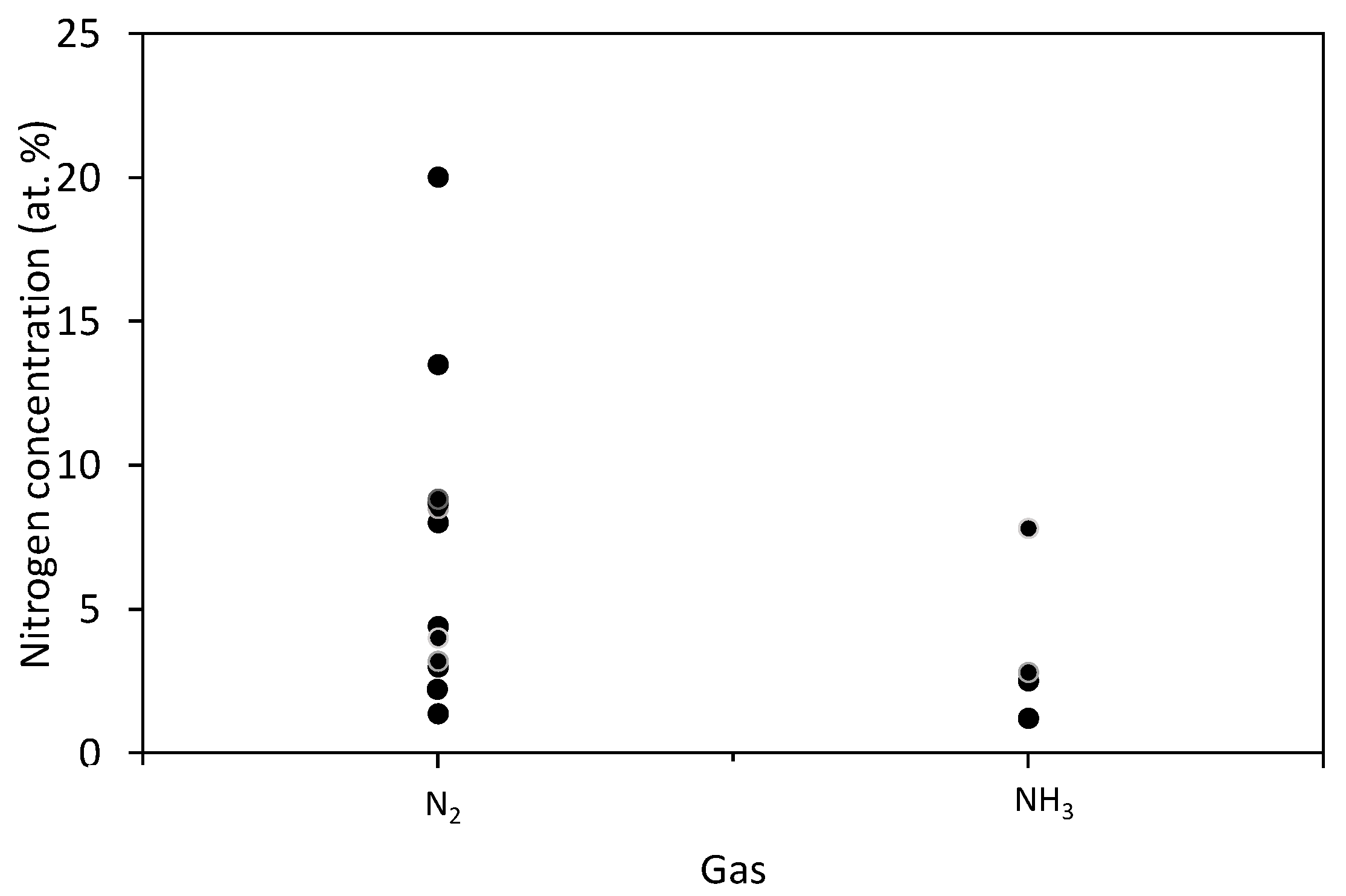
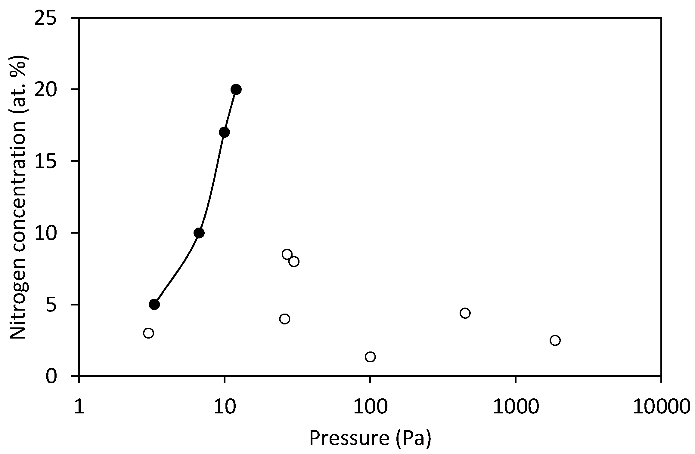
Systematic investigation of N-doping versus treatment parameters were provided in several papers. For example, the discharge power was varied systematically in [19,26], pressure in [27], and treatment time [1,11,24]. It should be stressed that such systematic experiments take time, especially spectra acquisition and the interpretation. Comparison of surface finishes obtained by different gases (N2 and NH3) using the same experimental system was reported in [29].
(5)
Nitrogen content in graphene-like materials is generally higher when using N2-plasma than NH3-plasma. Furthermore, in addition to pyridinic, pyrrolic, and graphitic nitrogen, the presence of amino groups was reported for NH3-plasma treatments.
It is difficult to draw any clear correlation between the nitrogen concentration, its configuration, and final properties of N-doped graphene-like materials, for example its conductivity. e.g., Cho et al. found an increased conductivity of N-doped CNWs in comparison to pristine CNWs [12]. They also found that the conductivity was decreasing with increasing nitrogen content in the range of N/C from 9.5 to 22%). Different results were reported by Santhosh et al. [29], who found decreasing conductivity of N-doped CNWs for both N2- and NH3-plasma treatment, where the maximum nitrogen content was 8 and 2.8 at.% for N2 and NH3 plasma, respectively. No correlation between the measured conductivity and nitrogen content was found by Santhosh et al.
The results summarized in Table 3 hardly reveal any correlation between the treatment parameters and reported concentration of nitrogen in various binding sites. Despite the fact that no direct comparison is possible because of various discharge parameters, we nevertheless present the results from Table 3 graphically in Figure 2, Figure 3, Figure 4, Figure 5 and Figure 6. Many authors reported increased N-concentration with increased treatment time at their particular conditions. This is shown in Figure 2. From Figure 2 we can also see scattering of measured points obtained by between different authors, meaning that treatment time is not the only decisive parameter. When comparing applications of N2 or NH3 gas (Figure 3), it seems that more nitrogen is introduced into the graphene structure if authors used N2 gas. Furthermore, in the case of ammonia, authors reported the presence of amino groups [29]. There is also no clear correlation versus the gas pressure (Figure 4) and discharge power (Figure 5), although one might speculate that the N concentration is increasing with increasing power and pressure as found by some authors at their particular conditions. Nevertheless, scattering of the results can be explained as a consequence of a different concentrations and doses of reactive plasma species in the discharge operating at different powers, pressures, or treatment times. In Figure 6 is shown the reported N/C ratio versus two parameters, i.e., plasma treatment time and discharge power, but also here there is no clear correlation.
Finally, we should also mention the problems associated with a uniform modification of vertically-oriented graphene (CNWs). As already mentioned, such structures are typically first deposited in an atmosphere free from nitrogen, followed by a post-treatment with plasma sustained in N2 or NH3. The interaction of reactive species from nitrogen plasma with CNWs can be predicted using the schematic illustration in Figure 7. Depending on discharge parameters, there are many reactive species in nitrogen plasma, such as positively charged ions, metastable molecules, and neutral atoms. The uppermost graphene sheets are subjected to a larger flux of ions than those deep in the film. Furthermore, if the sheets are not perfectly perpendicular (very likely), the surfaces not facing plasma are not affected by ions at all. Opposite to ions, the atoms do not feel the electric field and they can move randomly, as shown schematically in Figure 7. Because the distance between the neighboring sheets is smaller than the mean free path, the collisions with surfaces will prevail. Even if the probability for recombination of N atoms is low, the huge number of collisions will create a large gradient of N-atoms across the film. In one experiment, it has been shown that the CNWs exhibit an extremely high recombination coefficient for oxygen atoms because of the porous structure [45]. The coefficient for nitrogen atoms has never been reported, but in analogy with oxygen, it can be assumed that the loss of N atoms by surface recombination to parent molecules is also large enough to create strong gradients of N atoms across the CNW film. As a result, it can be expected that CNWs deep below the surface will be under-treated.
Gradients in both positive ions and atoms are therefore likely to occur upon treatment of CNWs or similar materials with nitrogen plasma. The result is the overtreatment of the surface layer (which may lead to etching) and undertreatment of the graphene sheets deep in the structure. It is expected that the N concentration in the graphene network will be high on the surface and negligible close to the interface with the substrates. Unfortunately, we have not found a single paper on the depth profiling of CNWs to reveal uniformity of modification versus depth. Any problems with gradients are avoided if a one-step procedure is accomplished. To the best of our knowledge, no report on the growth of vertically oriented graphene structures rich in nitrogen has appeared in the scientific literature. A possible explanation is a well-known fact that any attempt to use a mixture of hydrocarbon gas and nitrogen at low pressure leads preferentially to the formation of HCN molecules rather than the deposition of nitrogenated carbon nanostructures.

6. Conclusions and Perspectives

N-doped graphene-like materials can be synthesized by different techniques. The most straight-forward one is chemical vapor deposition: gaseous precursors are introduced into a furnace where they gradually decompose due to high temperature and a film containing carbon and other elements grows on a substrate. This procedure will normally lead to the formation of a rather compact film, so it is used predominantly for deposition of horizontally oriented films. The technique is scalable but not very interesting for application in electrochemical devices where an extremely high surface-to-mass ratio is required. Most authors used techniques based on the application of gaseous plasma.
Gaseous plasma can be used for one-step synthesis, which is typically performed by introducing a mixture of gaseous precursors into the plasma reactor. Methane (or any other light hydrocarbon) is used as a source of carbon, and nitrogen or ammonia gas is a source of nitrogen in the graphene-like film. This technique also seems to be useful only for deposition of horizontally-oriented structures.
Three-dimensional structures of N-doped graphene-like materials of high porosity are preferably synthesized using a two-step procedure. In the first step, carbon nanowalls free from nitrogen are deposited using a PECVD technique, and these materials are then functionalized with nitrogen in the second step, where plasma free from hydrocarbons is used. The three-dimensional carbon nanomaterials are doped with nitrogen at various experimental configurations, from nitrogen or ammonia afterglows (where pure chemical interaction occurs) to biased samples where ion implantation is the predominant mechanism.
The properties of N-doped graphene-like materials vary significantly depending on their structure, which is related to the method used for their synthesis. One limitation of the methods is their ability to produce N-doped samples with controllable concentration and configuration of nitrogen, and another limitation is the upscaling of the method to mass production on the industrial scale. Two-step procedures are too time-consuming to be interesting for the industrial production of N-doped CNWs. Direct one-step procedures are thus much better alternatives. However, enabling deposition on large surface areas and line-production still remains a challenge.
The science of N-doped vertically-oriented graphene structures is still in its infancy. Numerous authors have used different plasma techniques for synthesizing such materials, which are desired in several applications, in particular the fuel cells, batteries, and supercapacitors. The obtained structures differ significantly, so no correlation between the processing parameters and the resultant structures could be drawn on the basis of reviewed literature. The concentration of nitrogen in the materials probed by XPS was from less than 1 at.% and up to about 20 at.%. Typically, it was about a few at.%. No clear correlation between the amount of nitrogen and improved characteristics of N-doped graphene samples was found. Even when nitrogen concentrations were very low at about 1 at.%, the authors reported improved characteristics of the samples. In addition, too high nitrogen concentration may again be not good enough. Several types of chemical bonds between N-atoms in the graphene structure have been confirmed. At the current level of the state-of-the-art, it is not possible to deduce the processing parameters that would lead to preferential incorporation of N-atoms to a specific binding site; therefore, this still remains a scientific challenge. The review also reveals that most authors investigated the N-incorporation in the surface film as probed by XPS and Raman spectroscopy. The results may not be representative for thick films of vertically-oriented graphene because strong gradients of fluxes of reactive nitrogen particles are expected.
The synthesis of vertically oriented N-doped graphene such as nanowalls, nanomesh, or similar morphological forms on the surface of a smooth substrate is currently limited to a two-step procedure. In the first step, a film containing nitrogen-free carbon structures is deposited, preferably by PECVD, and in the next step, the structures are exposed to nitrogen plasma. A one-step procedure currently enables deposition of horizontally oriented graphene structures of limited applicability. There is a need for inventing a method for a one-step deposition because the gradients in nitrogen concentration could be suppressed if not avoided using such a technique. Any attempt to deposit vertically oriented N-doped carbon nanostructures using hydrogenated carbon precursors in plasma with nitrogen or ammonia admixtures failed, probably due to preferential etching and formation of volatile hydrogen cyanide.
The deposition of vertically oriented carbon nanostructures with an appropriate concentration of nitrogen in various chemical bonds remains a scientific challenge. In order to enlighten the kinetics of the formation of various nitrogen configurations in graphene structure, the correlations between the fluxes and/or fluences of reactive nitrogen plasma particles and surface finish are desired. Once the correlations are known, further studies will be necessary to form desired structures in a controllable and repeatable manner.

Author Contributions

Conceptualization, A.V.; methodology, A.V., R.Z. and G.P.; formal analysis, R.Z.; investigation, A.V.; resources, A.V.; data curation, R.Z.; writing—original draft preparation, A.V.; writing—review and editing, M.M., G.P. and R.Z.; supervision, M.M.; project administration, G.P.; funding acquisition, A.V. All authors have read and agreed to the published version of the manuscript.

Funding

This research was funded by the financial support from the Slovenian Research Agency—project No. L2-1834 (Carbon nanowalls for future supercapacitors).

Conflicts of Interest

The authors declare no conflict of interest. The funders had no role in the design of the study; in the collection, analyses, or interpretation of data; in the writing of the manuscript, or in the decision to publish the results.

Abbreviations

CNWsCarbon nanowalls
ECRElectron cyclotron resonance
MWMicrowave
RFRadiofrequency
ICInductively coupled
APPJAtmospheric-pressure plasma jet
CVDChemical vapor deposition
PECVDPlasma-enhanced chemical vapor deposition
RDERotating disk electrode
CVCyclic voltammetry
EISElectrochemical impedance spectroscopy
STMScanning tunneling microscopy
TEMTransmission electron spectroscopy
XPSX-ray photoelectron spectroscopy
AFMAtomic force microscopy
AAFMAcoustic atomic force microscopy
ARPESAngle-resolved photoemission spectroscopy
NEXAFSNear-edge X-ray absorption fine structure
SAEDElective area electron diffraction
XRDX-ray diffraction
SPEMScanning photoemission microscopy
UPSUltraviolet photoelectron spectroscopy
ARIPESAngle-resolved inverse photoemission spectroscopy
LEEDLow-energy electron diffraction
WCAWater contact angle measurements
OESOptical emission spectroscopy
FTIRFourier-transform infrared spectroscopy
ORROxygen reduction reaction

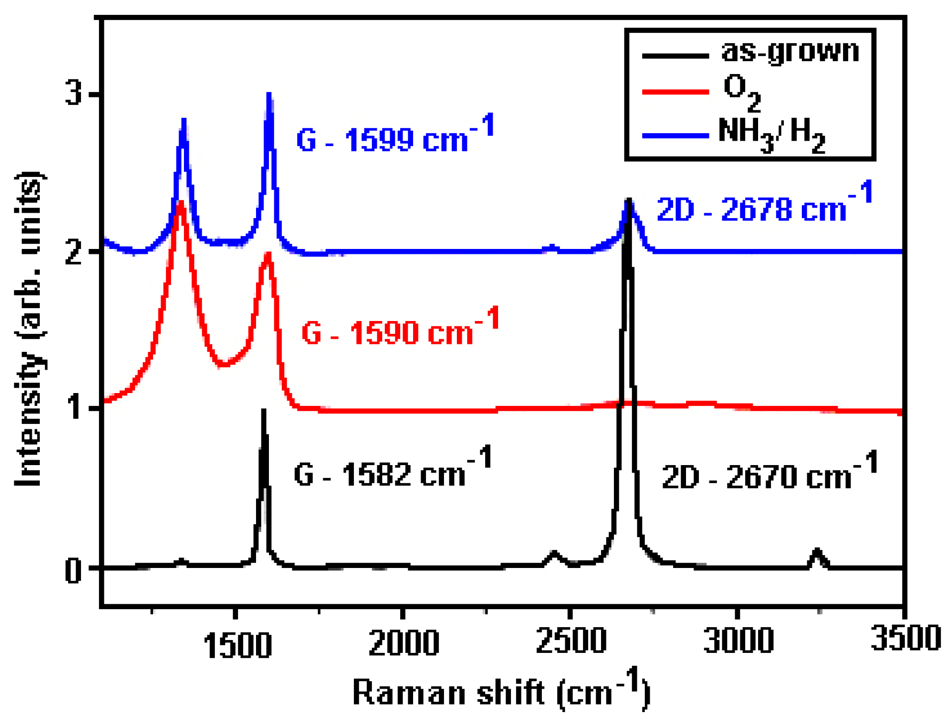
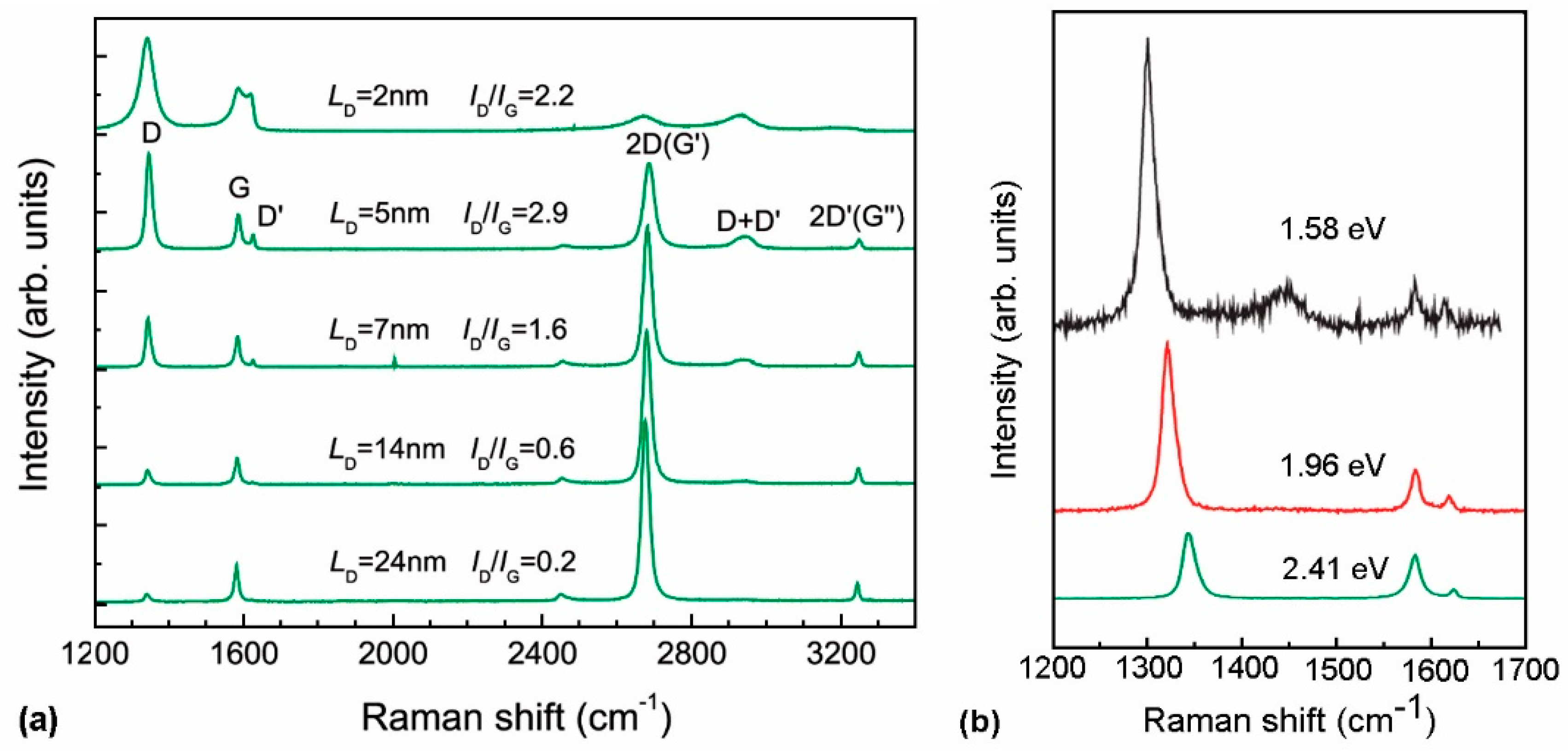
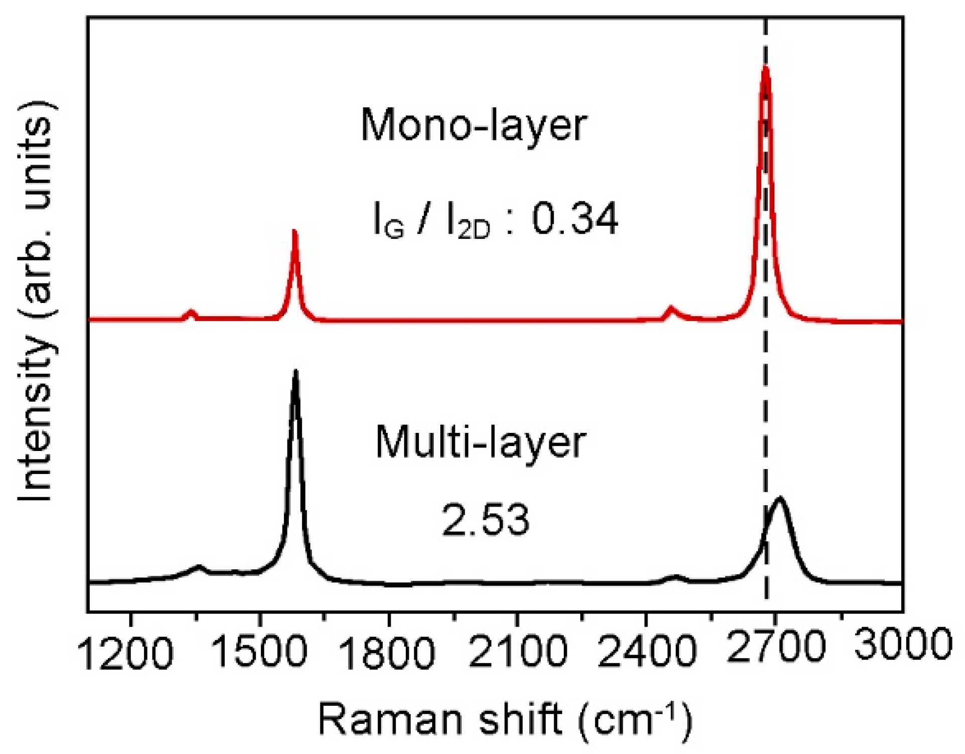
Appendix A. Raman Spectroscopy of Graphene-Like Materials

Raman spectroscopy is an important technique for surface characterization of carbon-based materials. A typical Raman spectrum of CNWs, graphene and other nanocarbon structures is shown in Figure A1. Raman spectrum of graphene shows two characteristic peaks, i.e., graphitic G band at about ~1580 cm−1 and 2D band at about ~2700 cm−1. The 2D band is the second-order band (sometimes also marked as G'). The 2D band is always observed for graphene, no matter if a D band is visible or not. The D band (~1350 cm−1), which is related to the presence of defects, is usually very weak in graphene samples because of a low number of defects [46].
Figure A1. (a) Raman spectra of CNWs (Reproduced from [47] (Hiramatsu et al.) under CC Attribution 3.0), and (b) comparison of Raman spectra of various types of sp2 nanocarbon configurations such as graphene, HOPG (highly-oriented pyrolytic graphite), SWNT (single-walled nanotube), SWNH (Single-walled nanohorn), and amorphous sp3 carbon. Reprinted with permission from Dresselhaus et al. [48] Copyright 2020 American Chemical Society.
Nanomaterials 10 02286 g0a1
Raman spectra of various forms of carbon may significantly differ, as shown in Figure A1. The Raman spectra of CNWs are similar to the spectrum of a damaged graphene. Opposite to the spectrum of graphene, they show many second-order modes and disorder-induced features [48]. CNWs and doped graphene with many defects, thus exhibit the significant intensity of D band along with G and 2D bands. With increasing D band intensity, another D' band also appears (~1620 cm−1). The D' band is associated with a finite size of graphite crystals and edges of graphene sheets [49]. The D' band is positioned close to the G band and is often observable as a knee on the G band curve because of partial overlapping. Moreover, the position of the G band is shifted upward [50]. An example of this is shown in Figure A2, where a comparison of Raman spectra of graphene, graphene treated in O2 plasma, and oxygen-plasma pretreated graphene which was further treated in NH3 plasma is shown [51]. The 2D band is much lower in cases of post-treatment in comparison to pristine graphene.
Figure A2. Raman spectra of pristine graphene, graphene treated with O2 plasma, and O2 plasma-treated graphene after additional treatment in NH3/H2 plasma. Reprinted from McEvoy et al. [51]. Copyright 2020, with permission from Elsevier.
Nanomaterials 10 02286 g0a2
Lucchese et al. [52] investigated the evolution of graphene when exposed to Ar+ ion bombardment for various doses from 1011 and up to 1015 cm−2 to induce defects. The energy of ions was 90 eV. While only the G band was observed for the pristine graphene, the D band appeared on irradiated samples, as shown in Figure A3. The intensity of the D band was increasing with increasing ion dose. With increasing D-band intensity, also D’ became apparent, and its intensity was also increasing. For the highest doses above 1014 cm−2, the intensity of all peaks decreased, and they became wider, indicating amorphization or partial sputtering of graphene despite the rather low kinetic energy of Ar+ ions adopted in that study.
Figure A3. Evolution of Raman spectra of graphene samples exposed to Ar ions. The ions doses are in units of cm−2. Reprinted from Lucchese et al. [52]. Copyright 2020, with permission from Elsevier.
Nanomaterials 10 02286 g0a3
The intensity of the D band for CNWs and doped graphene samples with many defects is much higher than the intensity of the G band. Therefore, the intensity ratio of ID/IG is an important parameter [50,53], because the samples containing many defects and nanocrystalline samples will have a high ID/IG ratio. Increasing the ID/IG ratio also causes a broadening of peaks; therefore, FWHM (full width at half maximum) can be correlated with the structural disorder [53]. The ID/IG ratio is inversely proportional to the size of the crystallites La, as observed by Tuinstra and Koenig [54]. A large ID/IG ratio is related to smaller crystallites that cause a higher amount of boundary defects. The empirical relation between La and ID/IG was first proposed by Knight and White. The relation was valid only for the laser wavelength of 514.5 nm [55]. This is because the position of D and 2D bands, as well as the ratio ID/IG, depends on the excitation laser wavelength [53,56]. Therefore, ID/IG ratio is a function of both the crystallite size La and the laser wavelength:
I D I G = f ( L a , λ )
An example of the dependence of ID/IG on the crystallite size and wavelength is shown in Figure A4, as reported by Conçado et al. [53]. Conçado et al. [57] improved the Knight-White relation for the determination of La using various excitation laser wavelengths. They proposed the following equation for the crystallite size [57]:
L a ( nm ) = ( 2.4 × 10 10 ) λ 4 ( I D I G ) 1
where ID/IG is the ratio of integrated intensities of D and G bands and λ is the excitation laser wavelength (nm). An example of the dependence of ID/IG with La is shown in Figure A5. We can see that Equation (A2) is valid only for La greater than about 4 nm.
Figure A4. (a) Raman spectra of ion-bombarded single-layered graphene samples with different interdefect distance, and (b) Raman spectra of ion-bombarded single-layered graphene measured at different excitation laser wavelengths (laser energies). Reprinted with permission from [53] (Conçado et al.) Copyright (2020) American Chemical Society.
Nanomaterials 10 02286 g0a4
Figure A5. The ID/IG ratio of mono-layered graphene samples (using a λ = 514 nm laser) versus the distance between defects induced by ion bombardment. Reprinted from Lucchese et al. [52]. Copyright 2020, with permission from Elsevier.
Nanomaterials 10 02286 g0a5
As shown by Cançado et al. [53], ID/IG ratio can also be used for the calculation of the density (ND) of the point defects in graphene with LD > 10 nm by using the following equation:
N D ( cm - 2 ) = ( 1.8 ± 0.5 ) × 10 22 λ 4 ( I D I G )
Besides the ID/IG ratio, also I2D/IG and ID/ID' can give additional information. Das et al. [58] have shown that the ratio I2D/IG depended on the doping level. The authors showed clear graphical dependence of the ratio of I2D/IG peak intensities versus the electron concentration. It was also reported that the characteristics of the 2D band depend on the number of graphene layers; however, as reported by Das et al., the I2D/IG should not be used to estimate the number of graphene layers. Nevertheless, in multilayered graphene, changes in width, position, and especially the shape of the peak were observed with the increasing number of layers, as shown in Figure A6 and Figure A7. Also, a change in the ratio of 2D to G is observed (Figure A6). Lee et al. [28] obtained I2D/IG ≈ 2.94 and 0.39 for monolayer and multilayer graphene, respectively. Terasawa et al. have found that I2D/IG was decreasing with increasing nitrogen content, whereas ID/IG was more or less constant [16]. He explained this by the growth of multilayered graphene with smaller grain size. Small I2D/IG ratio and large ID/IG might be, in combination with Equation (A2), associated with a multilayered structure with small grains.
Figure A6. An example of the Raman spectrum of mono- and multi-layer graphene showing different 2D to G ratio. Reprinted from Lee et al. [28]. Copyright 2020, with permission from Elsevier.
Nanomaterials 10 02286 g0a6
Figure A7. Changes in the shape of the 2D band measured for single, double, triple, and four-layered graphene samples. Reprinted from Malard et al. [59]. Copyright 2020, with permission from Elsevier.
Nanomaterials 10 02286 g0a7
Substantial doping of graphene may induce severe damage of the graphene structure. As graphite is very close in the structure to graphene, we may use a model proposed by Ferrari et al. [50] to investigate modified graphene-like materials. The authors proposed a 3-stage model for the evolution of Raman spectra of graphite during its structural transformation. Stage 1 covers the transformation of graphite to nanocrystalline graphite, stage 2 deals with the transformation of nanocrystalline graphite to low-sp3 amorphous carbon, whereas stage 3 deals with the transformation to high-sp3 amorphous carbon. The intensity of ID/IG and the G position is changing during this transformation, as illustrated in Figure A8. The correlation observed for stage 1 and 2 is also relevant for CNWs and graphene samples with defects. We can see that in stage 1, both the position of G and ID/IG are increasing, whereas, in stage 2, the opposite is observed, i.e., they both decrease.
Figure A8. Amorphization trajectory showing the dependence of G-band position and ID/IG for various sp3 contents during the transition between different stages. Reprinted with permission from Ferrari et al. [50]. Copyright (2020) by the American Physical Society.
Nanomaterials 10 02286 g0a8
Raman spectra of nanocrystalline graphene samples with a low contribution of some sp3 carbon will thus show a shift of G band back to lower values, a decrease of the ratio ID/IG, and a loss of the second-order features [53]. Further investigation of Raman characteristics of the transition between stages 1 to 2 was performed by Eckmann et al. [60]. They investigated the intensity of D, G, D' and 2D bands as well as the ID/ID' ratio of oxidized graphene versus plasma treatment time and observed the transition from stage 1 to stage 2 (Figure A9). In stage 1, there was no difference when plotting the variation of the peak intensity or integrated peak areas, because the trend was the same. However, in stage 2, different behavior of the maximum intensity or integrated area with treatment time was observed because of compensation of intensity and increment of FWHM. This indicates that in stage 1, it is not so important if the ratio is calculated from maximum intensities or integrated areas. However, in stage 2, peak areas are more representative. The ID/IG ratio in stages 1 or 2 may be the same, but not FWHM. Therefore, FWHM, which is much larger in stage 2, can give additional information on the stage [53]. According to Figure A9 we can also observe significant trends of various bands in stage 1 or 2, which are summarized in Table A1. Eckmann also found that in stage 1, D and D' are proportional, and the proportionality factor depends on the type of defects in the sample [60]. For sp3 defects ID/ID' ≈ 13, for vacancy-like defects ID/ID' ≈ 7, and for boundary defects ID/ID' ≈ 3.5.
Figure A9. Difference between maximum and integrated peak intensities-variation of Raman intensities of characteristic bands versus plasma treatment time, showing the transition from stage 1 to stage 2: (a) maximum peak intensities, and (b) integrated peak areas. We can observe that in stage 2, there is a difference in the behavior of maximum intensities or integrated areas, especially of the G and D peaks. Reprinted with permission from [60] (Eckmann et al.). Copyright (2020) American Chemical Society.
Nanomaterials 10 02286 g0a9
Table A1. Behavior of Raman D, D', 2D, and G bands in stages 1 and 2, according to Eckmann [60].
D BandD’ Band2D BandG Band
Stage 1increaseincreasedecrease~constant
Stage 2decreaseincreasesharp decreaseintensity decrease, area increase
All the above-cited observations are summarized in Figure A10. According to Ferrari [50], the transition between stages 1 and 2 for graphite is observed at ID/IG ≈ 2; however, Eckmann et al. [60] observed this transition at ID/IG ≈ 4 for oxidized graphene obtained by plasma treatment at several exposure times.
Figure A10. The most important steps in the evolution of Raman spectra for the case, when graphite is changed to nanocrystalline graphite (stage 1) or from nanocrystalline graphite to low sp3 amorphous carbon (stage 2).
Nanomaterials 10 02286 g0a10

Appendix B. X-ray Photoelectron Spectroscopy of Graphene-Like Materials

XPS is another technique that can give additional information regarding the quality of carbon nanostructures and the presence of heteroatoms as well as the type of functional groups that were formed during the modification of graphene samples. Carbon C1s peak of a pure graphite-like sample with a high sp2 content, such as graphene, will have a strong asymmetric peak, described by its asymmetry factor α. Furthermore, several π-type shake-up satellite features are present and positioned several eV at higher binding energies from the main C1s peak (Figure A11). Satellite features for graphite were in detail described by Leiro et al. [61]. Also, the presence of any functional group will influence the shape of the C1s peak.
Figure A11. Position of satellites, its relative intensity and FWHM for HOPG. Reprinted from Leiro et al. [61]. Copyright 2020, with permission from Elsevier.
Nanomaterials 10 02286 g0a11
The main C1s peak of graphite-like materials is positioned at approximately ~284.4 eV [62]. The materials with high sp3 content will have a more symmetric peak, which is also slightly shifted to higher energy. Modified (doped) graphene samples will thus have a contribution of both asymmetric sp2 component (graphitic carbon) and symmetric sp3 component (defects) as well as the presence of additional symmetric peaks because of the covalently linked functional groups. This combination of asymmetric and symmetric components complicates the fitting of the C1s spectra, which is not straightforward. Therefore, the determination of sp2/sp3 contributions as regularly performed in published literature is often questionable. Furthermore, the spectrum C1s belonging to the sp2 component should be fitted with an asymmetric peak, whereas other subcomponents with symmetric peaks. However, the asymmetry is often neglected in the scientific literature. The asymmetry of the sp2 component shape can be determined on a reference sample. As a reference, often HOPG (highly-oriented-pyrolytic graphite) is used; however, we should be aware that the asymmetry of the sample with defects may change [63].
As already mentioned, many authors often simplify the fitting procedure by using only symmetric peaks, often taking into account also different peak widths. Furthermore, satellite features on the high-binding energy side of the spectrum several eV from the main C1s peak are sometimes not considered. It has been shown that the spectra of satellite features of graphite, diamond, and amorphous carbon differ in the shape and position [64] and even for the same material such as HOPG, depending on the sample preparation [63]. By neglecting the peak asymmetry and broad satellite features, the authors often fit a high-binding energy side of the spectrum with carbon-oxygen groups, whose presence is therefore questionable and the number of these groups and their concentration is overestimated. Furthermore, as shown by Bertoti et al. [7], the complexity caused by the peak asymmetry and its neglecting in the fitting procedure, the presence of various oxygen and nitrogen bonds, interaction among these moieties, etc. leads to significant scattering in the binding energy values of assigned peaks as shown in Figure A12.
Figure A12. Binding energies of the C1, O1s, and N1s of various carbon nanomaterials as reported by several researchers (red bars) and the ones obtained by Bertoti et al. for multilayered graphene and HOPG treated in nitrogen plasma (blue bars). Bertoti et al. determined peak asymmetry from HOPG reference and strictly limit the peak widths of all subpeaks. Reprinted from Bertoti et al. [7]. Copyright 2020, with permission from Elsevier.
Nanomaterials 10 02286 g0a12
A good example of the overestimation of the sp3 and oxygen content because of using conventional symmetric functions was given by Kovtun et al. In Figure A13 is shown a comparison of the fitting of the C1s peak of graphene using a conventional symmetric and asymmetric approach. We can see that the sp3 content, as well as oxygen content, were significantly overestimated on account of lower sp2 content if the symmetric fitting was used.
Susi et al. [62] presented a review of reported binding energies of the main C1s peak, their FWHM (full-width at half maximum), and the asymmetry index for various graphitic carbon nanomaterials. They also reported that a shift of the C 1s peak position to higher binding energies was observed upon nitrogen doping. The C1s shift was in the range between 0.1 to 0.4 eV. They also pointed out the problems of the broad range of the binding energies that were reported for various N1s configurations.
Blume et al. [63] presented an overview of problems associated with XPS analysis of carbon samples and how to identify and distinguish carbon species from their oxygen functionality. The authors showed how C1s spectra of HOPG, mono- and few-layer graphene, graphene flakes, graphene oxide, and single- and multi-wall carbon nanotubes differ in the binding energy, width, and shape of the peak, although the samples are “similar”. Many factors can have an impact on the line shape of the peak and its position, like surface contamination, the presence of disorder carbon, layer-to-layer interactions, and substrate interactions, topographic effects, etc. Fujimoto et al. [65] reported that also charging may significantly influence the assignment of the sp3 peaks because there are some reports where sp3 was found at lower binding energy than sp2. However, as shown by Blume et al. [63], sputtering of HOPG may result in broadening of the C1s on the high- as well as at low-binding energy side pointing out the different nature of these defects. These two different contributions can be assigned to disordered carbon and defect-like carbon. An example of the influence of disordered carbon and defects on the shape of C1s spectra is shown in Figure A14. This figure shows oxygen-free HOPG after sputtering using different sputter parameters to induce defects. With increasing accelerating voltage or ion dose, a broadening appears on the high binding-energy side (disordered C) as well as a shoulder at the low binding-energy side (defects). A similar observation was reported by other authors as well [14].
Figure A13. Comparison of the results obtained by the fitting procedure using: (a) the conventional symmetric approach and (b) another approach by considering sp2 asymmetry for graphene sample prepared by CVD. (c) When using symmetrical fit as often adopted by researchers, the sp3 and oxygen content are overestimated. Reprinted from Kovtun et al. [66]. Copyright 2020, with permission from Elsevier.
Nanomaterials 10 02286 g0a13
Because of the uncertainties in the determination of the sp2 and sp3 content in the C1s spectra, some authors tried to use the so-called D-parameter, which is defined as the energy distance between the minimum and maximum of the first derivatives of Auger C KLL spectra (1190–1250 eV) [65,67,68]. The higher D-parameters are related to a higher amount of sp2. The D-parameter for graphite is thus larger than for diamond, i.e., D ≈ 21 and D ≈ 14 for graphite and diamond, respectively [67,69]. The major problem is associated with defining the right maximum/minimum of the smoothed spectra. Bundaleska et al. [14] measured the C KLL spectra for N-doped graphene (Figure A15) after applying smoothing with 11 successive moving averages and obtained the D-value of 20.6 eV, which is close to the value as reported by Kaciulis and Mezzi for graphite [67,69].
Figure A14. A rise of disordered and defect like carbon peaks in C1s spectra recorded for HOPG exposed to sputtering with the kinetic energy of 150 eV using different accelerating voltage or ion dose (time). Reprinted from Blume et al. [63]. Copyright 2020, with permission from Wiley.
Nanomaterials 10 02286 g0a14
In the case of doping of graphitic samples with nitrogen, N1s is the most important XPS peak of investigation. As already mentioned in the introduction and shown in Figure 1, nitrogen in N-doped graphene samples can be found in various configurations like pyridinic, pyrrolic, graphitic nitrogen, and oxidized nitrogen groups. An example of the nitrogen N1s spectrum with subcomponents corresponding to different nitrogen configurations in N-doped graphene is shown in Figure A16. The reported range of the binding-energy (BE) values for various nitrogen configurations are shown in Table A2. Yamada et al. [70] reported calculated values for the peak shifts and their FWHMs. They found that the average shift of the BE values of N1s reported by other authors is quite well correlated with their calculations for some functional groups, including pyridinic, pyrrolic, and quaternary nitrogen. They also reported that functional groups originating from edges have lower FWHM than those originating from the basal planes. Zhang et al. [13] noticed a shift of the N1s peak position with the growth temperature of N-doped graphene synthesized at, what was explained by different local environment of N atoms because of formation of defects.
Figure A15. C KLL region in the XPS spectra of N-doped graphene. Reprinted from Bundaleska et al. [14] under the terms of the Creative Commons CC BY license from Springer Nature.
Nanomaterials 10 02286 g0a15
Figure A16. An example of N1s spectra of N-doped graphene. Reprinted from Maddi et al. [71] under the terms of the Creative Commons CC BY license from Springer Nature.
Nanomaterials 10 02286 g0a16
Table A2. Reported values of binding energies of various nitrogen configurations.
Pyridinic
(N1)
Pyrrolic
(N2)
Graphitic/Quaternary
(N3)
AmineOxidized FormsRef.
398.3399.7400.9 [7]
398.7400.2402.3 [14]
398.6400.1401.1 [33]
398.9400.2401.7 [12]
398.7400.1401.8 [31]
398.5–398.6399.6–399.8401.1 [18]
398.4399.9401.2 [72]
398.5400.1401.5 [23]
398.2400.1401.7399.0 [28]
~398~400~401 [32]
398.7400.3401.4~400.3402–405[19]
398.9400.1401.1 402.6[11]
398.7400.3401.2 402.8[43]
398.5399.9401 [41]
399.4/401.2 [15]
398.9400.1401.5 [42]
398.3400.5/ [4]
398.9399.6401.2 [40]
398.4// [20]
///399.6 [21]
398.2400.3401.5 [44]
/399.3/ [34]
398.3–398.4399.6–399.9400.9–402.4 405.6–406.1[13]
For graphene samples treated in ammonia plasma, sometimes also amino groups were reported (Table A2); however, because of its overlapping pyrrolic group, its presence cannot be unambiguously confirmed. An exception is a publication by Baraket et al. [27], who proved their presence by chemical derivatization; however, no details were given.
Despite all the problems regarding XPS characterization, as stated above, XPS is still an indispensable method for the characterization of graphene-like materials; however, it is sometimes difficult to compare quantitative results from the literature because the authors use a different way of presenting their results. This is evident from the review of the N-doped graphene synthesis procedures summarized in Table 1 and Table 2, and particularly in Table 3. We also noticed that nitrogen concentration is often given in “percentage”; however, sometimes it is not clear if the reported value is N/C ratio or N concentration in atomic percent. Furthermore, the concentration of other elements is often not stated, neither details about fitting procedure described.

References

  1. Evlashin, S.A.; Fedorov, F.S.; Dyakonov, P.V.; Maksimov, Y.M.; Pilevsky, A.A.; Maslakov, K.I.; Kuzminova, Y.O.; Mankelevich, Y.A.; Voronina, E.N.; Dagesyan, S.A.; et al. Role of nitrogen and oxygen in capacitance formation of carbon nanowalls. J. Phys. Chem. Lett. 2020, 11, 4859–4865. [Google Scholar] [CrossRef] [PubMed]
  2. Xu, H.; Ma, L.; Jin, Z. Nitrogen-doped graphene: Synthesis, characterizations and energy applications. J. Energy Chem. 2018, 27, 146–160. [Google Scholar] [CrossRef] [Green Version]
  3. Mahmood, N.; Zhang, C.Z.; Yin, H.; Hou, Y.L. Graphene-based nanocomposites for energy storage and conversion in lithium batteries, supercapacitors and fuel cells. J. Mater. Chem. A 2014, 2, 15–32. [Google Scholar] [CrossRef] [Green Version]
  4. Qu, L.; Liu, Y.; Baek, J.-B.; Dai, L. Nitrogen-doped graphene as efficient metal-free electrocatalyst for oxygen reduction in fuel cells. ACS Nano 2010, 4, 1321–1326. [Google Scholar] [CrossRef] [PubMed]
  5. Vesel, A.; Zaplotnik, R.; Primc, G.; Mozetič, M. Synthesis of vertically oriented graphene sheets or carbon nanowalls—Review and challenges. Materials 2019, 12, 2968. [Google Scholar] [CrossRef] [PubMed] [Green Version]
  6. Schiros, T.; Nordlund, D.; Pálová, L.; Prezzi, D.; Zhao, L.; Kim, K.S.; Wurstbauer, U.; Gutiérrez, C.; Delongchamp, D.; Jaye, C.; et al. Connecting dopant bond type with electronic structure in N-doped graphene. Nano Lett. 2012, 12, 4025–4031. [Google Scholar] [CrossRef]
  7. Bertóti, I.; Mohai, M.; László, K. Surface modification of graphene and graphite by nitrogen plasma: Determination of chemical state alterations and assignments by quantitative X-ray photoelectron spectroscopy. Carbon 2015, 84, 185–196. [Google Scholar] [CrossRef] [Green Version]
  8. Boas, C.R.S.V.; Focassio, B.; Marinho, E.; Larrude, D.G.; Salvadori, M.C.; Leão, C.R.; dos Santos, D.J. Characterization of nitrogen doped graphene bilayers synthesized by fast, low temperature microwave plasma-enhanced chemical vapour deposition. Sci. Rep. 2019, 9, 13715. [Google Scholar] [CrossRef]
  9. Usachov, D.; Vilkov, O.; Grüneis, A.; Haberer, D.; Fedorov, A.; Adamchuk, V.K.; Preobrajenski, A.B.; Dudin, P.; Barinov, A.; Oehzelt, M.; et al. Nitrogen-doped graphene: Efficient growth, structure, and electronic properties. Nano Lett. 2011, 11, 5401–5407. [Google Scholar] [CrossRef]
  10. Zhao, L.; He, R.; Rim, K.T.; Schiros, T.; Kim, K.S.; Zhou, H.; Gutiérrez, C.; Chockalingam, S.P.; Arguello, C.J.; Pálová, L.; et al. Visualizing individual nitrogen dopants in monolayer graphene. Science 2011, 333, 999–1003. [Google Scholar] [CrossRef] [Green Version]
  11. Singh, G.; Sutar, D.S.; Botcha, V.D.; Narayanam, P.K.; Talwar, S.S.; Srinivasa, R.S.; Major, S.S. Study of simultaneous reduction and nitrogen doping of graphene oxide Langmuir-Blodgett monolayer sheets by ammonia plasma treatment. Nanotechnol. 2013, 24, 11. [Google Scholar] [CrossRef] [PubMed]
  12. Cho, H.J.; Kondo, H.; Ishikawa, K.; Sekine, M.; Hiramatsu, M.; Hori, M. Effects of nitrogen plasma post-treatment on electrical conduction of carbon nanowalls. Jpn. J. Appl. Phys. 2014, 53, 4. [Google Scholar] [CrossRef]
  13. Zhang, J.; Zhao, C.; Liu, N.; Zhang, H.; Liu, J.; Fu, Y.Q.; Guo, B.; Wang, Z.; Lei, S.; Hu, P. Tunable electronic properties of graphene through controlling bonding configurations of doped nitrogen atoms. Sci. Rep. 2016, 6, 28330. [Google Scholar] [CrossRef] [PubMed]
  14. Bundaleska, N.; Henriques, J.; Abrashev, M.; Botelho do Rego, A.M.; Ferraria, A.M.; Almeida, A.; Dias, F.M.; Valcheva, E.; Arnaudov, B.; Upadhyay, K.K.; et al. Large-scale synthesis of free-standing N-doped graphene using microwave plasma. Sci. Rep. 2018, 8, 12595. [Google Scholar] [CrossRef] [Green Version]
  15. Tatarova, E.; Dias, A.; Henriques, J.; Abrashev, M.; Bundaleska, N.; Kovacevic, E.; Bundaleski, N.; Cvelbar, U.; Valcheva, E.; Arnaudov, B.; et al. Towards large-scale in free-standing graphene and N-graphene sheets. Sci. Rep. 2017, 7, 10175. [Google Scholar] [CrossRef]
  16. Terasawa, T.-O.; Saiki, K. Synthesis of nitrogen-doped graphene by plasma-enhanced chemical vapor deposition. Jpn. J. Appl. Phys. 2012, 51, 055101. [Google Scholar] [CrossRef]
  17. Kumar, A.; Voevodin, A.A.; Paul, R.; Altfeder, I.; Zemlyanov, D.; Zakharov, D.N.; Fisher, T.S. Nitrogen-doped graphene by microwave plasma chemical vapor deposition. Thin Solid Films 2013, 528, 269–273. [Google Scholar] [CrossRef]
  18. Evlashin, S.A.; Maksimov, Y.M.; Dyakonov, P.V.; Pilevsky, A.A.; Maslakov, K.I.; Mankelevich, Y.A.; Voronina, E.N.; Vavilov, S.V.; Pavlov, A.A.; Zenova, E.V.; et al. N-doped carbon nanowalls for power sources. Sci. Rep. 2019, 9, 6716. [Google Scholar] [CrossRef]
  19. McClure, J.P.; Thornton, J.D.; Jiang, R.Z.; Chu, D.; Cuomo, J.J.; Fedkiw, P.S. Oxygen reduction on metal-free nitrogen-doped carbon nanowall electrodes. J. Electrochem. Soc. 2012, 159, F733–F742. [Google Scholar] [CrossRef]
  20. Yen, H.F.; Horng, Y.Y.; Hu, M.S.; Yang, W.H.; Wen, J.R.; Ganguly, A.; Tai, Y.; Chen, K.H.; Chen, L.C. Vertically aligned epitaxial graphene nanowalls with dominated nitrogen doping for superior supercapacitors. Carbon 2015, 82, 124–134. [Google Scholar] [CrossRef]
  21. Zhao, C.X.; Zhang, Y.; Deng, S.Z.; Xu, N.S.; Chen, J. Surface nitrogen functionality for the enhanced field emission of free-standing few-layer graphene nanowalls. J. Alloys Compd. 2016, 672, 433–439. [Google Scholar] [CrossRef]
  22. Achour, A.; Solaymani, S.; Vizireanu, S.; Baraket, A.; Vesel, A.; Zine, N.; Errachid, A.; Dinescu, G.; Pireaux, J.J. Effect of nitrogen configuration on carbon nanowall surface: Towards the improvement of electrochemical transduction properties and the stabilization of gold nanoparticles. Mater. Chem. Phys. 2019, 228, 110–117. [Google Scholar] [CrossRef]
  23. Jeong, H.M.; Lee, J.W.; Shin, W.H.; Choi, Y.J.; Shin, H.J.; Kang, J.K.; Choi, J.W. Nitrogen-doped graphene for high-performance ultracapacitors and the importance of nitrogen-doped sites at basal planes. Nano Lett. 2011, 11, 2472–2477. [Google Scholar] [CrossRef] [PubMed]
  24. McManus, J.B.; Hennessy, A.; Cullen, C.P.; Hallam, T.; McEvoy, N.; Duesberg, G.S. Controlling defect and dopant concentrations in graphene by remote plasma treatments. Phys. Status Solidi B-Basic Solid State Phys. 2017, 254, 1700214. [Google Scholar] [CrossRef]
  25. Lin, Y.-P.; Ksari, Y.; Prakash, J.; Giovanelli, L.; Valmalette, J.-C.; Themlin, J.-M. Nitrogen-doping processes of graphene by a versatile plasma-based method. Carbon 2014, 73, 216–224. [Google Scholar] [CrossRef]
  26. Zeng, J.J.; Lin, Y.J. Tuning the work function of graphene by nitrogen plasma treatment with different radio-frequency powers. Appl. Phys. Lett. 2014, 104, 233103. [Google Scholar] [CrossRef]
  27. Baraket, M.; Stine, R.; Lee, W.K.; Robinson, J.T.; Tamanaha, C.R.; Sheehan, P.E.; Walton, S.G. Aminated graphene for DNA attachment produced via plasma functionalization. Appl. Phys. Lett. 2012, 100, 233123. [Google Scholar] [CrossRef]
  28. Lee, B.-J.; Cho, S.-C.; Jeong, G.-H. Atmospheric pressure plasma treatment on graphene grown by chemical vapor deposition. Curr. Appl. Phys. 2015, 15, 563–568. [Google Scholar] [CrossRef]
  29. Santhosh, N.M.; Filipic, G.; Kovacevic, E.; Jagodar, A.; Berndt, J.; Strunskus, T.; Kondos, H.; Hori, M.; Tatarova, E.; Cvelbar, U. N-graphene nanowalls via plasma nitrogen incorporation and substitution: The experimental evidence. Nanomicro Lett. 2020, 12, 53. [Google Scholar] [CrossRef] [Green Version]
  30. Manojkumar, P.A.; Krishna, N.G.; Mangamma, G.; Albert, S.K. Understanding the structural and chemical changes in vertical graphene nanowalls upon plasma nitrogen ion implantation. Phys. Chem. Chem. Phys. 2019, 21, 10773–10783. [Google Scholar] [CrossRef]
  31. Deng, D.; Pan, X.; Yu, L.; Cui, Y.; Jiang, Y.; Qi, J.; Li, W.-X.; Fu, Q.; Ma, X.; Xue, Q.; et al. Toward N-doped graphene via solvothermal synthesis. Chem. Mater. 2011, 23, 1188–1193. [Google Scholar] [CrossRef]
  32. Lu, Y.-F.; Lo, S.-T.; Lin, J.-C.; Zhang, W.; Lu, J.-Y.; Liu, F.-H.; Tseng, C.-M.; Lee, Y.-H.; Liang, C.-T.; Li, L.-J. Nitrogen-doped graphene sheets grown by chemical vapor deposition: Synthesis and influence of nitrogen impurities on carrier transport. ACS Nano 2013, 7, 6522–6532. [Google Scholar] [CrossRef] [PubMed] [Green Version]
  33. Amano, T.; Kondo, H.; Takeda, K.; Ishikawa, K.; Hiramatsu, M.; Sekine, M.; Hori, M. Oxygen reduction reaction properties of nitrogen-incorporated nanographenes synthesized using in-liquid plasma from mixture of ethanol and iron phthalocyanine. Jpn. J. Appl. Phys. 2018, 57. [Google Scholar] [CrossRef]
  34. Luo, Z.; Lim, S.; Tian, Z.; Shang, J.; Lai, L.; MacDonald, B.; Fu, C.; Shen, Z.; Yu, T.; Lin, J. Pyridinic N doped graphene: Synthesis, electronic structure, and electrocatalytic property. J. Mater. Chem. 2011, 21, 8038–8044. [Google Scholar] [CrossRef]
  35. Sui, Y.; Zhu, B.; Zhang, H.; Shu, H.; Chen, Z.; Zhang, Y.; Zhang, Y.; Wang, B.; Tang, C.; Xie, X.; et al. Temperature-dependent nitrogen configuration of N-doped graphene by chemical vapor deposition. Carbon 2015, 81, 814–820. [Google Scholar] [CrossRef]
  36. Wei, D.; Liu, Y.; Wang, Y.; Zhang, H.; Huang, L.; Yu, G. Synthesis of N-doped graphene by chemical vapor deposition and its electrical properties. Nano Lett. 2009, 9, 1752–1758. [Google Scholar] [CrossRef] [PubMed]
  37. Dias, A.; Bundaleski, N.; Tatarova, E.; Dias, F.M.; Abrashev, M.; Cvelbar, U.; Teodoro, O.M.N.D.; Henriques, J. Production of N-graphene by microwave N2-Ar plasma. J. Phys. D Appl. Phys. 2016, 49, 055307. [Google Scholar] [CrossRef]
  38. Lin, Y.C.; Lin, C.Y.; Chiu, P.W. Controllable graphene N-doping with ammonia plasma. Appl. Phys. Lett. 2010, 96, 133110. [Google Scholar] [CrossRef]
  39. Kato, T.; Jiao, L.; Wang, X.; Wang, H.; Li, X.; Zhang, L.; Hatakeyama, R.; Dai, H. Room-temperature edge functionalization and doping of graphene by mild plasma. Small 2011, 7, 574–577. [Google Scholar] [CrossRef]
  40. Yang, W.; Xu, X.; Tu, Z.; Li, Z.; You, B.; Li, Y.; Raj, S.I.; Yang, F.; Zhang, L.; Chen, S.; et al. Nitrogen plasma modified CVD grown graphene as counter electrodes for bifacial dye-sensitized solar cells. Electrochim. Acta 2015, 173, 715–720. [Google Scholar] [CrossRef]
  41. Sim, U.; Yang, T.-Y.; Moon, J.; An, J.; Hwang, J.; Seo, J.-H.; Lee, J.; Kim, K.Y.; Lee, J.; Han, S.; et al. N-doped monolayer graphene catalyst on silicon photocathode for hydrogen production. Energy Environ. Sci. 2013, 6, 3658–3664. [Google Scholar] [CrossRef]
  42. Wang, Y.; Shao, Y.; Matson, D.W.; Li, J.; Lin, Y. Nitrogen-doped graphene and its application in electrochemical biosensing. ACS Nano 2010, 4, 1790–1798. [Google Scholar] [CrossRef] [PubMed]
  43. Shao, Y.; Zhang, S.; Engelhard, M.H.; Li, G.; Shao, G.; Wang, Y.; Liu, J.; Aksay, I.A.; Lin, Y. Nitrogen-doped graphene and its electrochemical applications. J. Mater. Chem. 2010, 20, 7491–7496. [Google Scholar] [CrossRef]
  44. Zhang, C.; Fu, L.; Liu, N.; Liu, M.; Wang, Y.; Liu, Z. Synthesis of nitrogen-doped graphene using embedded carbon and nitrogen sources. Adv. Mater. 2011, 23, 1020–1024. [Google Scholar] [CrossRef] [PubMed]
  45. Mozetic, M.; Vesel, A.; Stoica, S.D.; Vizireanu, S.; Dinescu, G.; Zaplotnik, R. Oxygen atom loss coefficient of carbon nanowalls. Appl. Surf. Sci. 2015, 333, 207–213. [Google Scholar] [CrossRef]
  46. Ferrari, A.C.; Meyer, J.C.; Scardaci, V.; Casiraghi, C.; Lazzeri, M.; Mauri, F.; Piscanec, S.; Jiang, D.; Novoselov, K.S.; Roth, S.; et al. Raman spectrum of graphene and graphene layers. Phys. Rev. Lett. 2006, 97, 187401. [Google Scholar] [CrossRef] [Green Version]
  47. Hiramatsu, M.; Kondo, H.; Hori, M. Nanoplatform Based on Vertical Nanographene. In Graphene-New Trends and Developments; Ebrahimi, F., Ed.; IntechOpen: Rijeka, Croatia, 2015. [Google Scholar] [CrossRef] [Green Version]
  48. Dresselhaus, M.S.; Jorio, A.; Hofmann, M.; Dresselhaus, G.; Saito, R. Perspectives on carbon nanotubes and graphene Raman spectroscopy. Nano Lett. 2010, 10, 751–758. [Google Scholar] [CrossRef]
  49. Hiramatsu, M.; Hori, M. Carbon nanowalls: Synthesis and Emerging Applications; Springer: Wien, Austria, 2010. [Google Scholar] [CrossRef]
  50. Ferrari, A.C.; Robertson, J. Interpretation of Raman spectra of disordered and amorphous carbon. Phys. Rev. B 2000, 61, 14095–14107. [Google Scholar] [CrossRef] [Green Version]
  51. McEvoy, N.; Nolan, H.; Kumar, N.A.; Hallam, T.; Duesberg, G.S. Functionalisation of graphene surfaces with downstream plasma treatments. Carbon 2013, 54, 283–290. [Google Scholar] [CrossRef]
  52. Lucchese, M.M.; Stavale, F.; Ferreira, E.H.M.; Vilani, C.; Moutinho, M.V.O.; Capaz, R.B.; Achete, C.A.; Jorio, A. Quantifying ion-induced defects and Raman relaxation length in graphene. Carbon 2010, 48, 1592–1597. [Google Scholar] [CrossRef]
  53. Cançado, L.G.; Jorio, A.; Ferreira, E.H.M.; Stavale, F.; Achete, C.A.; Capaz, R.B.; Moutinho, M.V.O.; Lombardo, A.; Kulmala, T.S.; Ferrari, A.C. Quantifying defects in graphene via Raman spectroscopy at different excitation energies. Nano Lett. 2011, 11, 3190–3196. [Google Scholar] [CrossRef] [PubMed] [Green Version]
  54. Tuinstra, F.; Koenig, J.L. Raman spectrum of graphite. J. Chem. Phys. 1970, 53, 1126–1130. [Google Scholar] [CrossRef] [Green Version]
  55. Knight, D.S.; White, W.B. Characterization of diamond films by Raman spectroscopy. J. Mater. Res. 2011, 4, 385–393. [Google Scholar] [CrossRef]
  56. Ferrari, A.C. Raman spectroscopy of graphene and graphite: Disorder, electron–phonon coupling, doping and nonadiabatic effects. Solid State Commun. 2007, 143, 47–57. [Google Scholar] [CrossRef]
  57. Cançado, L.G.; Takai, K.; Enoki, T.; Endo, M.; Kim, Y.A.; Mizusaki, H.; Jorio, A.; Coelho, L.N.; Magalhães-Paniago, R.; Pimenta, M.A. General equation for the determination of the crystallite size La of nanographite by Raman spectroscopy. Appl. Phys. Lett. 2006, 88, 163106. [Google Scholar] [CrossRef]
  58. Das, A.; Pisana, S.; Chakraborty, B.; Piscanec, S.; Saha, S.K.; Waghmare, U.V.; Novoselov, K.S.; Krishnamurthy, H.R.; Geim, A.K.; Ferrari, A.C.; et al. Monitoring dopants by Raman scattering in an electrochemically top-gated graphene transistor. Nature Nanotechnol. 2008, 3, 210–215. [Google Scholar] [CrossRef] [Green Version]
  59. Malard, L.M.; Pimenta, M.A.; Dresselhaus, G.; Dresselhaus, M.S. Raman spectroscopy in graphene. Phys. Rep. 2009, 473, 51–87. [Google Scholar] [CrossRef]
  60. Eckmann, A.; Felten, A.; Mishchenko, A.; Britnell, L.; Krupke, R.; Novoselov, K.S.; Casiraghi, C. Probing the nature of defects in graphene by Raman spectroscopy. Nano Lett. 2012, 12, 3925–3930. [Google Scholar] [CrossRef] [Green Version]
  61. Leiro, J.A.; Heinonen, M.H.; Laiho, T.; Batirev, I.G. Core-level XPS spectra of fullerene, highly oriented pyrolitic graphite, and glassy carbon. J. Electron Spectros. Relat. Phenom. 2003, 128, 205–213. [Google Scholar] [CrossRef]
  62. Susi, T.; Pichler, T.; Ayala, P. X-ray photoelectron spectroscopy of graphitic carbon nanomaterials doped with heteroatoms. Beilstein J. Nanotechnol. 2015, 6, 177–192. [Google Scholar] [CrossRef] [Green Version]
  63. Blume, R.; Rosenthal, D.; Tessonnier, J.-P.; Li, H.; Knop-Gericke, A.; Schlögl, R. Characterizing graphitic carbon with x-ray photoelectron spectroscopy: A step-by-step approach. ChemCatChem 2015, 7, 2871–2881. [Google Scholar] [CrossRef] [Green Version]
  64. Haq, S.; Tunnicliffe, D.L.; Sails, S.; Savage, J.A. Assessment of nondiamond carbon levels present in chemical vapor deposited diamond by analysis of the plasmon loss features of x-ray photoelectron spectra. Appl. Phys. Lett. 1996, 68, 469–471. [Google Scholar] [CrossRef]
  65. Fujimoto, A.; Yamada, Y.; Koinuma, M.; Sato, S. Origins of sp3C peaks in C1s X-ray photoelectron spectra of carbon materials. Anal. Chem. 2016, 88, 6110–6114. [Google Scholar] [CrossRef] [PubMed] [Green Version]
  66. Kovtun, A.; Jones, D.; Dell’Elce, S.; Treossi, E.; Liscio, A.; Palermo, V. Accurate chemical analysis of oxygenated graphene-based materials using X-ray photoelectron spectroscopy. Carbon 2019, 143, 268–275. [Google Scholar] [CrossRef] [Green Version]
  67. Mezzi, A.; Kaciulis, S. Surface investigation of carbon films: From diamond to graphite. Surf. Interface Anal. 2010, 42, 1082–1084. [Google Scholar] [CrossRef]
  68. Theodosiou, A.; Spencer, B.F.; Counsell, J.; Jones, A.N. An XPS/UPS study of the surface/near-surface bonding in nuclear grade graphites: A comparison of monatomic and cluster depth-profiling techniques. Appl. Surf. Sci. 2020, 508, 144764. [Google Scholar] [CrossRef]
  69. Kaciulis, S.; Mezzi, A.; Calvani, P.; Trucchi, D.M. Electron spectroscopy of the main allotropes of carbon. Surf. Interface Anal. 2014, 46, 966–969. [Google Scholar] [CrossRef]
  70. Yamada, Y.; Kim, J.; Matsuo, S.; Sato, S. Nitrogen-containing graphene analyzed by X-ray photoelectron spectroscopy. Carbon 2014, 70, 59–74. [Google Scholar] [CrossRef]
  71. Maddi, C.; Bourquard, F.; Barnier, V.; Avila, J.; Asensio, M.-C.; Tite, T.; Donnet, C.; Garrelie, F. Nano-architecture of nitrogen-doped graphene films synthesized from a solid CN source. Sci. Rep. 2018, 8, 3247. [Google Scholar] [CrossRef]
  72. Huang, L.; Cao, Y.; Diao, D. N-doped graphene sheets induced high electrochemical activity in carbon film. Appl. Surf. Sci. 2019, 470, 205–211. [Google Scholar] [CrossRef]
Figure 1. The most common bonding configuration of nitrogen atoms in graphene.
Nanomaterials 10 02286 g001
Figure 2. The reported N/C ratio versus the plasma treatment time.
Nanomaterials 10 02286 g002
Figure 3. The reported nitrogen concentration versus the gas type.
Nanomaterials 10 02286 g003
Figure 4. The reported nitrogen concentration versus the total gas pressure. Full symbols refer to the only more systematic study reported in [27], whereas empty symbols refer to several individual experiments of other authors mentioned in Table 3.
Nanomaterials 10 02286 g004
Figure 5. The reported nitrogen concentration versus the discharge power. Full symbols refer to two systematic investigations reported in [19,26], whereas empty symbols refer to several individual experiments of other authors mentioned in Table 3.
Nanomaterials 10 02286 g005
Figure 6. The reported N/C ratio versus two parameters, i.e., plasma treatment time and discharge power.
Nanomaterials 10 02286 g006
Figure 7. Schematic of the interaction between reactive nitrogen species and carbon nanowalls.
Nanomaterials 10 02286 g007
Table 1. Overview of published literature on post-synthesis of N-doped graphene.
RefMethodGasMaterialTreatment Parameters for
N-Doping
Methods for CharacterizationMost Important ConclusionsPossible
Application
[1]Post-plasma treatment N2, O2 or mixture O2:N2 = 25:75CNWsDC discharge, 2kV, 80 mA, pressure: 0.2 Torr, treatment time: 1–120 min (90 min)SEM, XPS, Raman (/), CV- 4 at.% N + 10 at.% O,
- increased specific capacitance
- ID/IG increased from 0.81 to 0.86,1.63, and 1.38 for O2, N2, and O2/N2, respectively;
- I2D/IG decreased from 0.95 to 0.72, 0.32, and 0.64 for O2, N2, and O2/N2, respectively,
- La decreased from 23.8 nm to 22.4, 11.8, and 14 nm for O2, N2, and O2/N2, respectively
supercapacitors
[18] Post-plasma treatment N2CNWsDC discharge,
pressure: 3 Pa,
treatment time: 2 h
SEM, XPS, Raman (/), electrochemical measurements3 at.% N + 30 at.% O
ID/IG increased from 0.78 to 0.90 after doping
supercapacitors
[12]Post-plasma treatment N2CNWsCCP plasma,
power: 400 W,
N2 flow 10 sccm,
treatment time: 30–300 s
OES, SEM, XPS, Raman (/), van der Pauw-Hall measurements Electrical properties depended on treatment time. N/C = 9.5% (30 s)–22.2% (300 s)electronic application
[19]Post-plasma treatment N2/Ar(1:2)CNWsPressure: 2 Pa,
RF power: 200, 300, 600 W, treatment time: 15 min
XPS, Raman (632.8 nm), TEM, RDE4–20 at.% of N
39–52 at.% of O,
A change of ID/IG after doping depended on the crystallite size La of non-doped CNWs.
Electrocatalyst for polymer electrolyte membrane fuel cells
[20]Post-plasma treatment NH3Vertical graphene nanowallsMW PECVD, In-situ doping after CNW synthesis using NH3SEM, TEM, XPS, Raman (532 nm), EIS, CV, galvanostatic measurements7.8 at.% of N—only pyridinic N was found.
Capacitance: 991.6 F/g,
Energy density: 275.4 Wh/kg,
Power density: 14.8 kW/kg
supercapacitors
[30]Ion implantationN2Vertical graphene nanowallsRF source of ions,
Sample biased with pulsed DC voltage of 2 kV;
Treatment time: 10, 20, 30 min
SEM, Raman (514.5 nm), XPS, AFM/AFAM7.6–8.8 at.% of N and ~13 at.% of O. Reduction of ID/IG from 2.5 to 1.3.
No modification in CNWs morphology up to 20 min.
/
[21]Post-plasma treatment NH3Vertically aligned few-layer
graphene (FLG)
PECVD, RF power: 20 W, pressure: 1.4 Torr, NH3 flow rate 50 sccm, substrate temperature: 350 °C, treatment time: 30 minSEM, TEM, XPS, Raman (514.5 nm), field emission properties1.2 at.% of N in the form of amino groups.
IG/I2D decreased from 1.53 to 1.03, whereas ID/IG increased from 1.94 to 2.20.
Lower work function and enhanced electron emission properties.
Field emitters
[22] Post*-plasma
treatment
*already pristine CNW contaminated with N
Ar/N2 or Ar/O2CNWsPECVD,
RF power 50 W
Ar flow 100 sccm,
N2 or O2 flow 10 sccm, pressure: 0.2 Pa, treatment time: 5 min
SEM, XPS, Raman (514 nm), CV, EIS12.5–13.5 at.% of N.
Pyrrolic N was found to be important for improvement of electrochemical transaction.
I2D/IG decreased from 0.5 to 0.4 and 0.2, whereas ID/IG decreased from 1.47 to 1.38 and 1.27 for Ar/N2 and Ar/O2, respectively
Electrochemical transductors
[23]Post-plasma treatment N2Graphene layerPECVD, power: 500 W, pressure: 14 Torr, flow rate 91 sccm, treatment time: up to 3 min followed by annealing at 300 °C for 3 hTEM, SAED, XRD, SPEM, Raman (/), CV,
galvanostatic measurements
1.7–2.5 at.% of N,
16–25 at.% of O,
capacitance 4× larger than for the undoped graphene (280 F/gelectrode), excellent cycle life
ultracapacitors
[11]Post-plasma treatment NH3Graphene oxide monolayerDC plasma,
power: 10 W,
pressure: 1 Pa,
treatment time 1–20 min
SEM, AFM, XPS, UPS, Raman (514 nm), electrical conductivityN/C = 6–25%, O/C = 15–27%.
Pyridinic, pyrrolic, and graphitic N content depended on treatment time.
The best results obtained at low treatment time (n-type). ID/IG increased from 1.5 to 1.9 only for long times.
/
[24]Post-plasma treatment Ar followed by NH3/H2GrapheneMW, remote two-step procedure: Ar plasma (60 s), followed by NH3/H2 (300 s), Ar flow = 200 sccm (2 Torr), NH3 flow = H2 flow = 50 sccm (1 Torr), sample position 30 cm downstream XPS, Raman (532 nm), electrical measurements2.5 at.% of N, n-type
I2D/IG = 1.2, ID/IG = 0.02 for pristine graphene.
After Ar treatment ID/IG ~ 2.5, after Ar/NH3/H2 treatment ID/IG ~ 1
transistors
[37] Post-plasma treatment Ar/N2Self-standing graphene sheetsMW power 600 W,
Pressure: 100 Pa, total flow 50 sccm, N2:Ar = 10:90, treatment time: 5, 10, and 15 min
Raman (633 nm), XPS, TEM, OESPyridinic, pyrrolic and quaternary N,
high doping level 5.6%,
increase of sp2/sp3 ratio
/
[38]Post-plasma treatment NH3Bilayer grapheneDose: 3 × 1014 cm−2, other details not specifiedXPS, Raman (633 nm) Doping level: 1.5 × 1013 cm−2.
I2D/IG changed from 1.7 to 0.7
/
[39]Post-plasma treatment NH3Graphene sheetRF 13.56 MHz, with/without an additional Cu grid in the discharge tube after the coil. Power 20 (45 W) with (without) a grid. Remote treatment at a distance 75 (45) cm and treatment time 60 (10) min with (without) a grid.AFM, Raman (632.8 nm), electrical measurementsGraphene preferably doped near the edge. Doping density: 1.7 × 1012 cm−2 for mild treatment (with a grid)./
[25]Post-plasma treatment N2Graphene monolayerTunable hybrid ECR-MW plasma source, two modes of operation: (1) an ion-mode with a flux: 4 × 10¹² ions s−1 cm−2, energy 35 eV, and (2) an atom-mode (by using an ion trap) with a flux of atoms 2.5 × 10¹⁵ s−1 cm−2, sample at 850 °C, pressure 5 × 10⁻⁵ mbar, treatment time: 10 minARIPES, XPS, LEEDIon-mode treatment: n-type dopping attributed to 8.7 at.% of graphitic N.
Atom-mode treatment:mainly pyridinic N is formed, minor n-doping
/
[40]Post-plasma treatment N2Few-layer grapheneIon irradiation, DC power supply, negative bias 300–350 V, pressure: 460 Pa, treatment time: 20 and 40 sXPS, Raman (532 nm), TEM, EIS4.4 and 2.8 at.% of N for 40 and 20 s.
Mostly pyridinic and pyrrolic N, graphitic only in a minor concentration.
3-times higher energy conversion efficiency.
Solar cells
[28]Post-plasma treatment N2Mono-, few-, and multi-layer grapheneAPPJ (15 kV, 25 kHz, AC), flow rate 15 slm, APPJ positioned in N2 surrounding atmosphere, treatment times: 1–30 s, jet distances from the sample: 1, 2, 3 cmXPS, TEM, WCA, Raman (532 nm)Pyridinic nitrogen prevailed.
ID/IG increased with plasma treatment time from 0.22 to 0.6.
Surface change to hydrophilic (contact angle 44°) because of the OH and COOH groups.
/
[41]Post-plasma treatment N2Monolayer grapheneRF plasma 13.56 MHz, power: 10 W,
pressure: 0.12 Torr,
treatment time: 0–16 s
XPS, Raman (514.5 nm), CV, RDEPyridinic N prevailed, followed by pyrrolic and graphitic N.
Enhanced electrocatalytic activity and charge transfer.
Hydrogen production
[42]Post-plasma treatment N2GrapheneHarrick model PDC-32G plasma cleaning unit, power: 100 W, pressure: 0.75 Torr, treatment time: 20, 40, 60, 100 minXPS, TEM, CV, 1.35 at.% of N and 28 at.% of O.
High electrochemical activity for reduction of H2O2.
Fast direct electron transfer kinetics for glucose oxidase
Biosensors
[43]Post-plasma treatment N2Graphene sheetPC2000—Plasma Cleaner, RF 13.56 MHz, power 140 W, pressure: 0.2 Torr, treatment time: 20 min,
DC bias 990 V
XPS, Raman (514.5 nm), ORR, CV8.5 at.% of N and 8.6 at.% of O.
Nitrogen was in all typical configurations with the highest pyrrolic content.
Higher electrochemical activity toward oxygen reduction
ORR (fuel cells, biosensors)
[26]Post-plasma treatment N2Graphene filmsRF, powers: 30, 50, 70 W, flow rate: 50 sccm, pressure: 0.7 Pa,
treatment time: 5 min
XPS, Raman (532 nm), Scanning Kelvin Probe, Van der Pauw-Hall measurementsn-type, mostly graphitic N.
ID/IG increased from 0.42 to 0.45, 0.60, 0.81 for 30, 50, and 70 W, respectively.
Increased power caused increased graphitic content, increased electron concentration, and a shift of Fermi level to higher energy. Work function decreased.
optoelectronics
[27]Post-plasma treatment Ar/NH3 Graphene filmsElectron beam plasma, 2 kV, 5% NH3,
pressure: 25–90 mTorr, total treatment time: 60 s (equivalent plasma exposure time 6 s)
XPS, Raman (/)N content increased with increasing pressure from 5 to 20 at.%.
Raman D peak also increased with pressure.
biosensors
[29]Post-plasma treatment N2 or NH3Graphene nanowallsIC RF, power: 300 W,
flow rate: 100 sccm, pressure: 30 Pa,
post-glow region i.e., 10 cm away from the glow, treatment time: 4, 8, 12, 25 s (for NH3) and 10, 20, 30, 40 s (for N2), pulsed treatment to keep the sample < 50 °C
XPS, SEM, NEXAFS, Raman (633 nm), van der Pauw measurements8.0 and 2.8 at.% of N for N2 and NH3, respectively.
All three N types were found as well as amine for NH3 treatment.
N2 caused etching, which was not observed for NH3.
ID/IG was in general decreasing with increasing treatment time: from 2.8 to 2.28 (40 s, N2) or to 2.68 (12 s, NH3).
/
Table 2. Overview of published literature on direct-synthesis of N-doped graphene.
RefMethodGas/PrecursorMaterialTreatment Parameters for
N-Doping
Methods for CharacterizationMost Important ConclusionsPossible
Application
[9]CVD s-triazineGraphene monolayervapor pressure: 1 × 10⁻⁶ mbar,
deposition time: 30 min, temperature: 540–635 °C.
XPS, ARPES, NEXAFS1–2 at.% of N (0.4 at.% of graphitic N)
Bandgap 0.2 eV
semiconductors
[14]Direct plasma synthesis Ethanol + NH3Free-standing
graphene
MW at atmospheric pressure, additional IR and UV treatment for sp2 C and N-type manipulation.
Deposition yield: 1.3 mg/min
XPS, SEM, TEM, Raman (633 nm), CV, van der Pauw method,
OES and FTIR
N/C = 0.4%,O/C = 1.5%ID/IG ~ 0.9 after irradiation;
Higher relative amount of pyridinic and pyrrolic N for the irradiated CNWs.
supercapacitors
[44]Thermal segregation Few-Layer grapheneAnnealing of a substrate consisting of N-containing boron and C-containing Ni filmsXPS, Raman (514.5 nm), AFM, electrical characteristic of fabricated field-effect transistorsHigher N doping caused lower La.
La reduced from 65 nm to 21 and 8 nm for N/C = 0.6 and 2.9%, respectively
Doping level 4 × 1013 cm−2, bandgap 0.16 eV,
n-type
nanoelectronics
[31]Chemical synthesisCCl4 + Li3NFew-layer grapheneReaction of CCl4 with Li3NSTM, TEM, XPS, Raman (633 nm), thermal stability testsN/C = 4.5–16.4%. In the sample with a high N content, pyridinic and pyrrolic N dominated (p-type). For the sample with a low N content, graphitic N dominated (n-type). nanoelectronics
[32]CVD 1,3,5-triazineGraphene sheetsChemical vapor deposition of 1,3,5-triazine to Cu substrate at different temperatures 700, 800 and 900 °CXPS, Raman (473 nm), AFM, SEM, TEM, electrical measurementsN/C = 2.1–5.6%.
A lwer temperature was favorable to obtain higher N doping. Increasing of N-doping content caused the transformation of p-type to n-type.
nanoelectronics
[4]CVD CH4 + NH3Few-layer grapheneNH3/CH4/H2/Ar = 10/50/65/200 sccm for 5 min, followed by NH3/Ar for another 5 min, temperature 1000 °CAFM, TEM, Raman (514.5 nm), XPS, SEM, XRD, RDE4 at.% of N, pyridinic, and pyrrolic N-configuration.
ID/IG = 0.06–0.25
Improved electrocatalytic activity and stability.
Fuel cells
[33]In-liquid plasma ethanol + Fe-phthalocy-anineNano-graphenesIn-liquid plasma synthesis from ethanol and Fe-phthalocyanineSEM, XPS, Raman (/), ORR, CV6–11 at.% of N, N-configurations: pyridinic, Fe-N, pyrrolic and graphitic.
ID/IG = 1.25–1.66, La = 11.6–15. 3 nm
Polymer electrolyte fuel cells
[16]PECVD H2/CH4/N2Mono- to multilayer grapheneFlow rates of H2/CH4/N2 = 20/5/1 sccm. Power 300 W, pressure 1.08 Pa, growth time: 5 min, annealing to 500 and 950 °C.XPS, Raman (532 nm)N content: 0.5, and 1.1% at 950 and 500 °C, respectively. N mostly in the graphitic form.
I2D/IG = 2.1 (decreasing with N content).
ID/IG = 1–1.5.
An island like growth.
/
[17]PECVD H2/CH4/N2Few-layer grapheneMW, first H2/CH4 treatment at 500 W, followed by N2/CH4 treatment at 150 W. Pressure: 10 Torr, flow: H2 = CH4 = 10 sccm, N2 = 50 sccm. Total growth time: 5 min. Temperature: 800 °C.Raman (532 nm), XPS, SEM, TEM2 at.% of N in the form of pyridinic, graphitic, and oxygenated form.
ID/IG increased from 1.34 to 2.3, and I2D/IG decreased from 1.0 to 0.28.
/
[15]PECVD Ar/ethanol/N2
+UV
Free- standing
graphene
MW, power: 2 kW, Ar flow 1200 sccm, ethanol flow 15 sccm, N2 flow 5 or 10 sccmXPS, SEM, FTIR, NEXAFS, Raman (532 nm)0.2 at.% of N and 8 at.% of O,
mostly pyridinic nitrogen and some graphitic, growth yield 2 mg/min.
/
[8]PECVD H2/CH4/N2Graphene bilayersMW, power: 500 W,
N2:CH4 = 2:1, 3:1, or 5:1,
H2 flow: 10 sccm,
pressure: 43 Torr, deposition time: 2.5 min, temperature: 760 °C
XPS, Raman (532 nm), simulations2.0–4.2 at.% of N, pyridinic, and another peak related to other type of N defects. Formation of interlayer bonds mediated by nitrogen defects.
ID/IG increased from 0.6 to 2, I2D/IG decreased from 1.5 to 0.7.
/
[34]CVDH2/C2H4/
NH3
Single-layer
graphene
Thermal deposition in H2/C2H4/NH3 at various NH3 flow ratesXPS, Raman (532 nm), SIMS, UPS, RDE voltametryN/C = 1.6–16%. Depending on NH3 flow,
pure pyridinic N formation.
ORR
[35]CVDCH4/NH3Graphene domain filmThermal deposition in NH3 and CH4 at various temperatures 880–1050 °CXPS, Raman (532 nm)Control of N configuration by growth temperature. At high temperatures, mostly pyridinic N was formed, and pyrrolic N at low temperatures. The N concentration was decreasing with increasing temperature.
N = 4.5 and 0.7 at.% at 880 and 1050 °C, respectively.
/
[13]Free-radical reactionPenta-chloro-pyridineGraphene filmsFree-radical reaction from pentachloropyridine at various growth temperatures 230–600 °CXPS, Raman, STM, electronic propertiesControl of N configuration by growth temperature.
Graphitic N dominated at 230–300 °C and pyrrolic N at (400–600 °C).
ID/IG = 0.48–1.91 (minimum at 400 °C)
La = 7.4–19.6 nm
/
Table 3. Summary of discharge parameters and XPS results for the direct and post-plasma synthesis of N-doped graphene.
RefGasDischargeMaterialTreatment TimePowerPressure/FlowN and O Content as Obtained by XPS
[1]N2, O2, or mixtureDCCNWs1–120 min
(90 min)
0.2 TorrN: 4 at.%
O: 10 at.%
N/C = 4.7%
[18]N2DCCNWs2 h 3 PaN: 3 at.%
O: 30 at.%
N/C = 4.5%
[12]N2 CCPCNWs30, 180, 300 s400 W10 sccmN/C = 9.5% at 30 s
N/C = 16.4% at 180 s
N/C = 22.2% at 300 s
[19]N2/Ar RFCNWs15 min200, 300, and 600 W2 PaN: 5, 7, or 18 at.%,
O: 41, 52 or 39 at.%,
N/C = 9, 17 or 42%
for 200, 300 and 600 W, respectively (pristine CNW deposited at 860 °C).
N: 4, 6, or 20 at.%
O: 47, 45, 39 at.%
N/C = 8, 12 or 49%
for 200, 300 and 600 W, respectively (pristine CNW deposited at 730 °C)
[20]NH3MW PECVDVertical graphene nanowalls N: 7.8 at.%,
pyridinic N
[30]N2RF/DC
biased
Vertical graphene nanowalls10, 20, 30 min N: 7.6–8.8 at.%
O: ~13 at.%
N/C ~ 10%
[21]NH3RF PECVDVertically aligned few-layer
graphene (FLG)
30 min20 W1.4 Torr
50 sccm
N: 1.2 at.%,
amino groups
[22] Ar/N2 or Ar/O2RF PECVDCNWs5 min50 W0.2 Pa
100/10 sccm
N: 12.5–13.5 at.%
Pyridinic, pyrrolic, graphitic, and oxygenated N
[23]N2PECVDGraphene layer0.5–3 min + followed by annealing 3 h500 W14 Torr
91 sccm
N: 1.7 at.%, O: 25.5 at.%, N/C = 2.3% for 0.5 min
N: 1.9 at.%, O: 15.9 at.%, N/C = 2.3% for 1 min
N: 2.2 at.%, O: 21.8 at.%, N/C = 2.8% for 1.5 min
N: 2.4 at.%, O: 16.9 at.%, N/C = 3.0% for 2 min
N: 2.5 at.%, O: 19.6 at.%, N/C = 3.2% for 3 min
Pyridinic, pyrrolic and graphitic. Graphitic content was decreasing with increasing treatment time.
[11]NH3DCGraphene oxide monolayer1–20 min10 W1 PaN/C = 6%, O/C = 27%, for 1 min
N/C = 9%, O/C = 25% for 2 min
N/C = 15%, O/C = 15% for 5 min
N/C = 20%, O/C = 22% for 10 min
N/C = 25%, O/C = 26% for 20 min
Pyridinic, pyrrolic and graphitic
[24]Ar + NH3/H2MWGraphene60 s in Ar
+ 300 s in NH3/H2
1 Torr, 200/50/50 sccmN: 2.5 at.%
[37] Ar/N2MWSelf-standing graphene sheets5, 10, 15 min600 W100 Pa
45/5 sccm
N/C ~ 8%, O/C ~ 19% for 5 min
N/C ~ 4%, O/C ~ 26% for 10 min
N/C ~ 6%, O/C ~ 115% for 15 min
(estimated from the graph)
Pyridinic, pyrrolic, and graphitic N
[25]N2ECR-MWGraphene
monolayer
Two modes of operation:
(1) ion-mode, flux = 4 × 10¹² ions s−1 cm−2,
(2) atom-mode, flux = 2.5 × 10¹⁵ s−1 cm−2,
0.005 PaIon-mode treatment:
N: 8.7 at.%, mostly graphitic
Atom-mode treatment:
Minor doping, mainly pyridinic
[40]N2DC
biased
Few–layer graphene20 s, 40 s 460 PaN: 4.4 at.% at 40 s
N: 2.8 at.% at 20 s
Mostly pyridinic and pyrrolic, graphitic N in a minor concentration
[41]N2RFMonolayer graphene14 s10 W0.12 Torr2.2 at.%, pyridinic prevails, followed by pyrrolic and graphitic
[42]N2Harrick model PDC-32G plasma cleaning unitGraphene 20, 40, 60, 100 min100 W0.75 TorrN: 1.35 at.%
O: 28 at.%
N/C = 1.9%
[43]N2RF
biased
(PC2000—Plasma Cleaner)
Graphene sheets 20 min140 W 0.2 TorrN: 8.5 at.%
O: 8.6 at.%
N/C = 10%
Pyridinic, pyrrolic (the highest content), and graphitic
[26]N2RFGraphene films5 min30, 50, 70 W0.7 PaN: 2.5, 2.8 and 3.2 at.%, for 30, 50 and 70 W, respectively
Mostly graphitic
[27]Ar/NH3Electron beam plasmaGraphene filmstotal treatment time 60 s (equivalent plasma exposure time 6 s) 25–90 mTorrN: 5 at.% at 3.3 Pa
N: 10 at.% at 6.7 Pa
N: 17 at.% at 10 Pa
N: 20 at.% at 12 Pa
[29]N2 or NH3RFGraphene nanowalls4, 8, 12, 25 s
(for NH3)
10, 20, 30, 40 s (for N2)
300 W30 PaN: 8.0 and 2.8 at.% for N2 and NH3, respectively
Pyridinic, pyrrolic and graphitic N, as well as amine in the case of NH3 treatment
[14]EtOH/
NH3
MWFree-standing
graphene
/ AtmosphericN/C = 0.4%,
O/C = 1.5%
Higher amounts of pyridinic and pyrrolic N, if irradiated.
[33]EtOH and Fe-phthalo-cyanineIn-liquid plasmaNano-graphenes N: 6–11 at.%
Pyridinic, Fe-N, pyrrolic, and graphitic N
[16]H2/CH4/N2PECVDMono- to multilayer graphene5 min300 W1.08 PaN: 0.5%–1.1% for 950 and 500 °C, respectively
Mostly graphitic N.
[17]H2/CH4/N2PECVDFew-layer graphene5 min500 W10 Torr
10/10/50 sccm
N: 2 at.%
Pyridinic, graphitic and oxygenated N
[8]N2/H2/CH4MW PECVDGraphene bilayers2.5 min 500 W43 TorrN: 2.0 at.% for N2:CH4 = 2:1
N: 4.2 at.% for N2:CH4 = 3:1 and 5:1
Pyridinic N and another one related to other type of defects
[15]Ar/EtOH/N2 MW PECVD + UVFree- standing
graphene
/2000 W1200/15/(5 or 10) sccmN: 0.2 at.%
O: 8 at.%
Mostly pyridinic and some graphitic
Publisher’s Note: MDPI stays neutral with regard to jurisdictional claims in published maps and institutional affiliations.

